EP0809317A1 - Frequency multiplexing/demultiplexing of RF signal channels - Google Patents
Frequency multiplexing/demultiplexing of RF signal channels Download PDFInfo
- Publication number
- EP0809317A1 EP0809317A1 EP97302891A EP97302891A EP0809317A1 EP 0809317 A1 EP0809317 A1 EP 0809317A1 EP 97302891 A EP97302891 A EP 97302891A EP 97302891 A EP97302891 A EP 97302891A EP 0809317 A1 EP0809317 A1 EP 0809317A1
- Authority
- EP
- European Patent Office
- Prior art keywords
- transmission line
- band
- directional filter
- directional
- multiplexer
- Prior art date
- Legal status (The legal status is an assumption and is not a legal conclusion. Google has not performed a legal analysis and makes no representation as to the accuracy of the status listed.)
- Ceased
Links
Images


Classifications
-
- H—ELECTRICITY
- H01—ELECTRIC ELEMENTS
- H01P—WAVEGUIDES; RESONATORS, LINES, OR OTHER DEVICES OF THE WAVEGUIDE TYPE
- H01P1/00—Auxiliary devices
- H01P1/20—Frequency-selective devices, e.g. filters
- H01P1/213—Frequency-selective devices, e.g. filters combining or separating two or more different frequencies
- H01P1/2138—Frequency-selective devices, e.g. filters combining or separating two or more different frequencies using hollow waveguide filters
Definitions
- This invention relates to multiplexing/demultiplexing an FDM of RF signal channels.
- the invention is especially concerned with signal processing on artificial communications satellites, and particularly output multiplexing.
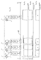
- a typical on-board system comprises a receiving antenna 1 and two transmitting antennas 2, 3.
- the transmitting antennas may point to different regions of the earth.
- the uplink signal received by the receiving antenna will be an FDM ( Figure 2) of n channels of a certain bandwidth and, after amplification by low noise amplifier 4, demultiplexer 5 separates the signal into n channels 6 1 -6 n (usually equispaced frequency slots) which are individually amplified by amplifiers such as travelling wave tubes 7 1 -7 n .
- the signal channels are multiplexed by launching electromagnetic radiation from each waveguide 12 1 -12 n into a waveguide manifold 13, short circuited at the end 13a at a respective precise distance from the short circuited end which is related to the wavelength, in order to produce standing waves in the waveguide 13.
- Each channel is filtered via a respective two-port filter 14 1 -14 n .
- the problem with such a design is that the filters have to be tuned in situ because the tuning of each filter affects the tuning of the others.
- each travelling wave tube amplifier 7 1 -7 n can be alternately connected to one of two ports on a single output multiplexer 15 by means of respective switches 16 1 -16 n .
- the signals enter the directional filter by one input port a, producing travelling waves propagating along the waveguide 18 of the output multiplexer 15, as shown in Figure 5, in a right hand direction to feed the antenna 2, while the left hand side of the waveguide 18 is terminated by the second antenna 3.
- the signals enter the directional filters by means of the other input port b, producing travelling waves propagating along the waveguide 18 of the output multiplexer 15 in the opposite direction to feed the second antenna 3, while the right hand side of the waveguide 18 is still terminated by the first antenna 2.
- Figure 6 shows the pass-band response of the filters when signals are fed in at port a for feeding antenna 2.
- the filter pass-bands are contiguous.
- the pass-band response (from a to d, and b to c) and band stop response (from a to b, and c to d) of one of the filters 17 (shown in Figure 7a) are shown in more detail in Figures 7b and 7c, respectively.
- the pass-band response of the filters is the same when signals are fed in at port b for feeding antenna 3.
- each channel is defined by a band pass filter with steeply descending transition regions in order to allow closely spaced narrow bands.
- directional filters employing a succession of cavities with more than one resonance per cavity has been disclosed (EP 0 249 612 B) with a quasi-elliptic response.
- EP 0 249 612 B it is a fundamental law that for minimum phase networks the narrower the bandwidth, the greater the variation of group delay across that bandwidth.
- the invention provides a multiplexer for producing an FDM of RF signal channels, comprising a transmission line, a plurality of directional filters by means of which respective signals can be coupled onto the transmission line, wherein at least one of the channels of the resulting FDM on the transmission line is defined at one edge by the band pass response of the directional filter coupling the respective signal onto the transmission line and at the other edge by the band stop response of another directional filter for coupling another signal onto the transmission line.
- each directional filter may now be greater than the signal channel, permitting a reduced variation of group delay across the bandwidth.
- the directional filters may be implemented as cavity resonators.
- An input and output dual-mode cavity resonator may be used to provide separate coupling paths into and out of a pair of quadruple-mode cavities which contain all the necessary mutual and cross-couplings to produce a desired elliptic response via longitudinal coupling slots only.
- the satellite on-board processing system which includes the output multiplexer is as shown in Figure 4 of the drawings.
- the output multiplexer ( Figure 8) consists of a transmission line in the form of a waveguide 18 connected to transmit antenna 2 at one end and a transmit antenna 3 at the other end.
- the multiplexer also includes n directional filters 17 1 -7 n , which are supplied via switches 16 1 -16 n which in turn are connected by waveguide to respective travelling wave tube amplifiers 7 1 -7 n which output the channels demultiplexed from the demultiplexer 5 of Figure 4. It is assumed that only channels 1-n are connected, channels 1'-n' will be referred to hereinafter.
- the filtering operation for each channel is performed by two directional filters and not one as hitherto.
- the pass-band of directional filter 17 1 from terminal a to terminal d ( Figure 9a) is approximately twice the desired width of the signal channel 1 ( Figure 9c), so that the signal passing along the waveguide 18 towards directional filter 17 2 actually overlaps signal channel 2.
- the frequency response of directional filter 17 2 between terminals c and d is a band-stop response ( Figures 7c and 9b).
- the lower frequency transition of the first channel 1 ( Figure 9c) is thus defined by the lower frequency transition of the pass-band of the first filter 17 1 , whereas the higher frequency transition of the first channel 1 is defined by the lower frequency transition of the band stop response of the second filter 17 2 .
- Each directional filter has a pass-band from a-d (or from b-c), and a band stop response from c-d or d-c with the same transition regions.
- the difference from the prior art arrangement of Figures 5 and 6 is that each pass-band/band stop region is wider in relation to the channel than hitherto (in this case, twice as wide), and adjacent passband/band stop regions overlap each other.
- the second channel 2 is defined in the same way as for the first channel, ie. by directional filters 17 2 (lower frequency edge) and by directional filters 17 3 (higher frequency edge). It will be observed that the last channel n will therefore be twice as wide as the other channels, since there is no adjacent band stop.
- the resulting FDM ( Figure 9c) is fed to antenna 2 for transmission.
- n' inputs produce n channels, in fact they do not occupy the frequency slots of their counterparts the inputs n.
- its output from input 2 falls in channel slot 2 (pass-band of 17 2 and band stop of 17 3 )
- its input (actually 3' ) now leaves port c and occupies channel slot 3 (pass-band of 17 2 but band stop of 17 1 ).
- each directional filter can be fed with two different channel slots simultaneously, and both antennas 2, 3 can be used simultaneously, each using the same set of frequency slots (apart from the differences at the ends noted above).
- the antennas are directed at different regions of the earth, twice as many signals can be broadcast as with the prior configuration of Figure 5, for the same number of filters and the same number of switches. (It would not be possible to feed both inputs of each filter of Figure 5 with signals occupying the same frequency slot to achieve the same result because there would be unacceptable crosstalk between the signals in the filters).
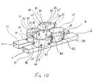
- Figure 10 shows the general arrangement of the four-port directional filter when implemented using multimode cavity resonators.
- the inputs a, b are connected to respective switches 16 1 , 16 2 etc, and the outputs c, d are joined to the outputs c, d of the next adjacent directional filters by extensions of the waveguide i.e. the output waveguide 18 is a continuous length of waveguide which includes a section c-d as shown in Figure 10 for each directional filter.
- the directional filter is formed by an input waveguide 22 and a parallel waveguide 21 which are interconnected by cylindrical cavity resonators 27 and 28 so that two distinct paths co-exist.
- the paths illustrated in the figure are, firstly, from input dual-mode resonator 27, coupled to the input waveguide 22, to quadruple-mode resonator 28, located on the output waveguide 21, then through to output dual-mode resonator 27, coupled to the output waveguide 21; secondly, input dual mode-resonator 27, coupled to the input waveguide 22, then to quadruple-mode resonator 28, located on the input waveguide 22, then to output dual-mode resonator 27, coupled to the output waveguide 21.
- the two paths should have identical electrical characteristics particularly in respect of signal phase shift and group delay.
- the arrangement illustrated is not a definitive embodiment, in terms of relative sizes and/or aspect ratio, but typifies the interconnection of a separate input and output waveguide with means which create two distinct filter paths each using at least one quadruple-mode cavity coupled only with longitudinal slots.
- cavity resonators 27 and 28 are of the form of right circular cylinders closed off at both ends.
- the input and output waveguides 22 and 21 are conventional rectangular conducting tubes suitably dimensioned so as to allow electromagnetic propagation in the dominant TE 10 waveguide mode.
- the input waveguide 22 has a pair of opposing ends a and b which serve as inputs of the directional filter and are used depending on the required signal flow direction through the filter.
- the output waveguide 21 has a pair of opposing ends c and d which serve as outputs from the directional filter depending on the required signal flow direction through the filter.
- an electromagnetic wave whose frequency falls in the pass-band of the filter, is input to one of the ends a, b of the input waveguide 22 and the filtered wave emerges from one of the opposing ends c, d of the output waveguide 21.
- an electromagnetic wave whose frequency does not fall in the pass-band of the filter, is input to one of the opposing ends of the input waveguide, it emerges only from the opposite end of the input waveguide to which it was input and so is passed on, unaffected, as an input to another such filter.
- the input waveguide is also a continuation of the waveguide sections a, b.
- the circular dual-mode cavity resonators 27 are dimensioned so as to support a TE 111 circularly polarised waveguide mode. Coupling into the input cavity 27, from the input rectangular waveguide 22, and out of the output cavity 27, into the output rectangular waveguide 21, is via an aperture suitably located to couple equal amounts of energy from the longitudinal and transverse components of the rectangular waveguides TE 10 dominant mode.
- This coupling aperture may be a simple circular hole 30 or another more complex aperture structure, as long as the resulting coupled components in the circular cavity resonator have a quadrature relationship in both time and space.
- These signals are the means of providing separate paths through the filter each being coupled into one of two quadruple-mode cavity resonators 28 the outputs of which are similarly coupled, by similar longitudinal slots 29, to the output cavity resonator 27 where the two signals are again recombined into a TE 111 circularly polarised wave.
- This wave is finally coupled into the output rectangular waveguide via a coupling aperture 30 which may be a simple circular hole or another more complex aperture structure.
- the mode configuration of the two quadruple-mode cavity resonators is illustrated in Figure 11 which shows arrows numbered 1-4 indicating the electric vectors of the four independent linearly polarised and orthogonal waves therein.
- the cavity must be suitably dimensioned so that it will support a pair of orthogonal TE 11N modes and a pair of orthogonal TM 110 modes.
- N can be any convenient integer value.
- the input and output longitudinal slots 29 1 and 29 2 respectively, orthogonally disposed and located in the cylindrical cavity wall, together with four additional couplings 37, 38, 39 and 40 formed by simple capacitive posts, or screws. Operationally, the magnetic field coupled from slot 29 1 will couple into the first TE 11N mode-1.
- coupling post, or screw, 38 at 45° to a common plane and at the intersection of the cylindrical wall and the cavities closed end, will further excite the first TM 110 mode-2.
- the inclusion of the coupling post, or screw, 39 at 45° to a common plane and at the intersection of the cylindrical wall and the closed end ofthe cavity, will couple into the second, and last, TE 11N mode-4.
- the energy of this fourth mode is coupled out of the cavity via the second longitudinal slot 29 2 excited by the magnetic field of this mode.
- the addition of coupling post, or screw, 40 forms a cross-coupling between the first and fourth TE 11N modes so that a symmetrical pair of finite frequency transmission zeros is produced.
- each separate filter path from input waveguide 22 to output waveguide 21, therefore makes use of at least one longitudinal, or transverse, resonance in the first dual-mode cavity 27, two TE and two TM modes in one of the quadruple-mode cavities 28, and one transverse, or longitudinal, resonance in the second dual-mode cavity 27.
- a symmetric pair of finite frequency transmission zeros is additionally produced by the cross-coupling post, or screw, 40 in the quadruple-mode cavity 28. Therefore, each path provides for at least six transmission poles together with a symmetric pair of finite frequency zeros, known as a quasi-elliptic transmission function, without the need for a cross-coupling via a separate cross-coupling aperture or slot.
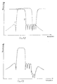
- the transmission function for filter 17 1 may be represented by the quasi-elliptical band-pass response as indicated by trace A in Figure 12. Due to the presence of the reflection-less termination port b of directional filter 17 2, the transmission function from c to d at directional filter 17 2, assuming a similar quasi-elliptical band-pass response for 17 2 as for 17 1 except for a displacement in pass-band centre frequency, will be that known as a band stop response typified by trace B in Figure 12. If the overlap in responses is equal to approximately half the transmission bandwidth then the overall transmission response from input a of 17 1 to d of 17 2 will be the product of A and B as shown in Figure 13.
- the new pass-band width is approximately half that of the original filter, the stop band response zeros of filter 17 2 have become transmission zeros in the overall response of filter 17 1 , and the high frequency roll-off region is entirely defined by the stop band characteristic of the next adjacent directional filter.
- a band-pass transmission response so produced provides for a number of advantages over conventional methods of channel definition, in terms of maintenance of signal fidelity provided by the transmission path from any input to the common output of the multiplexer, in as much as for the same shape factor, or selectivity, reduced pass-band amplitude and group delay variation is obtained.
- antenna 3 could be a receive antenna providing an FDM signal which, after low-noise amplification, would be fed along waveguide 18 and divided into respective signal channels 1-n.
- channel 1 would be defined by the full pass-band width of directional filter 17 1 , with signal energy entering port c and emerging from port b and thence from port 2' of switch 16 2 .
- Channel 2 would be defined by the part of the pass-band response of directional filter 17 2 which does not coincide with the band-stop response, from port c to d, of directional filter 17 1 .
- channel 2 is defined by the lower frequency corresponding to the upper stop-band edge of directional filter 17 1 , and the upper frequency corresponding to the upper pass-band of directional filter 17 2 . Therefore, received signals whose frequency components fall between these two limits are unaffected by the band-stop response of directional filter 17 1 , and so enter port c to emerge from port b of directional filter 17 2 and thence from port 3' of switch 16 3 .
- channel n is defined by the full pass-band width of directional filter 17 n whilst the remaining channels become defined as described previously.
- the invention is not restricted to directional filter illustrated in Fig. 10.
- the directional filter described in EP 0 249 612B could be used, or other types could be used.
- Typical frequencies of operation are microwave eg. 30MHz to 300GHz.
- each channel it is not necessary for each channel to represent one signal only. Two signals could be contained in one channel or, more generally, the channel could be digital, for example, time division multiplexed data.
- the filters it is not necessary for the filters to be physically positioned in the order of the channels they define. They could be physically positioned in any order, and the channels will be unaffected.
Landscapes
- Control Of Motors That Do Not Use Commutators (AREA)
- Variable-Direction Aerials And Aerial Arrays (AREA)
Abstract
A multiplexer comprises a number of directional filters 17n connected to a transmission line feeding an antenna 2, 3. Signals to be multiplexed fed to the filters 17n may be sent via respective switches 16n. Unlike prior multiplexers where each directional filter defines a respective channel of the multiplex, the channels of the multiplexer of the invention, apart from one at the end, are defined by the band pass response of one directional filter and the band stop response of another directional filter, since the band pass responses of the directional filters from the input connected to the switch to the output connected to the transmission line, and the corresponding band stop responses between the two output ports connected to the transmission line, overlap each other. The same arrangement may be used for demultiplexing.
Description
- This invention relates to multiplexing/demultiplexing an FDM of RF signal channels.
- The invention is especially concerned with signal processing on artificial communications satellites, and particularly output multiplexing.
- Referring to Figure 1, a typical on-board system comprises a receiving antenna 1 and two transmitting
antennas low noise amplifier 4,demultiplexer 5 separates the signal into n channels 61-6n (usually equispaced frequency slots) which are individually amplified by amplifiers such as travelling wave tubes 71-7n. These signals are then switched betweenoutput multiplexers 8, 9 feeding theantennas output multiplexers 8, 9 on the other hand by individual waveguide sections 111-11n and 121-12n, 131-13n. - Referring to Figure 3, which shows the circuit of the
output multiplexer 8, the signal channels are multiplexed by launching electromagnetic radiation from each waveguide 121-12n into awaveguide manifold 13, short circuited at theend 13a at a respective precise distance from the short circuited end which is related to the wavelength, in order to produce standing waves in thewaveguide 13. Each channel is filtered via a respective two-port filter 141-14n. The problem with such a design is that the filters have to be tuned in situ because the tuning of each filter affects the tuning of the others. - In order to overcome this, as well as to reduce the weight of the satellite, the use of directional filters (Figure 4, 5) has been proposed. With this arrangement, each travelling wave tube amplifier 71-7n can be alternately connected to one of two ports on a
single output multiplexer 15 by means of respective switches 161-16n. In the first switch position, the signals enter the directional filter by one input port a, producing travelling waves propagating along thewaveguide 18 of theoutput multiplexer 15, as shown in Figure 5, in a right hand direction to feed theantenna 2, while the left hand side of thewaveguide 18 is terminated by thesecond antenna 3. In the other switch position, the signals enter the directional filters by means of the other input port b, producing travelling waves propagating along thewaveguide 18 of theoutput multiplexer 15 in the opposite direction to feed thesecond antenna 3, while the right hand side of thewaveguide 18 is still terminated by thefirst antenna 2. - Figure 6 shows the pass-band response of the filters when signals are fed in at port a for
feeding antenna 2. The filter pass-bands are contiguous. The pass-band response (from a to d, and b to c) and band stop response (from a to b, and c to d) of one of the filters 17 (shown in Figure 7a) are shown in more detail in Figures 7b and 7c, respectively. The pass-band response of the filters is the same when signals are fed in at port b forfeeding antenna 3. - In the interests of maximising traffic carried by the on-board satellite signal processing system, each channel is defined by a band pass filter with steeply descending transition regions in order to allow closely spaced narrow bands. In order to achieve this, directional filters employing a succession of cavities with more than one resonance per cavity has been disclosed (EP 0 249 612 B) with a quasi-elliptic response. However, it is a fundamental law that for minimum phase networks the narrower the bandwidth, the greater the variation of group delay across that bandwidth.
- The invention provides a multiplexer for producing an FDM of RF signal channels, comprising a transmission line, a plurality of directional filters by means of which respective signals can be coupled onto the transmission line, wherein at least one of the channels of the resulting FDM on the transmission line is defined at one edge by the band pass response of the directional filter coupling the respective signal onto the transmission line and at the other edge by the band stop response of another directional filter for coupling another signal onto the transmission line.
- The pass band response of each directional filter may now be greater than the signal channel, permitting a reduced variation of group delay across the bandwidth.
- The directional filters may be implemented as cavity resonators. An input and output dual-mode cavity resonator may be used to provide separate coupling paths into and out of a pair of quadruple-mode cavities which contain all the necessary mutual and cross-couplings to produce a desired elliptic response via longitudinal coupling slots only.
- Multiplexers constructed in accordance with the invention will now be described, by way of example, with reference to the accompanying drawings, in which:
- Figure 1 illustrates a known satellite on-board repeater including two output multiplexers;
- Figure 2 illustrates schematically a frequency division multiplex;
- Figure 3 shows the circuit of the output multiplexers of Figure 1;
- Figure 4 shows a known satellite on-board repeater including a single directional output multiplexer;
- Figure 5 shows the circuit of the directional output multiplexer of Figure 4;
- Figure 6 shows the corresponding pass-bands of the directional filters of the output multiplexer of Figure 5;
- Figure 7a shows one of the directional filters of Figure 5 in more detail;
- Figure 7b shows the filter pass-band response from port a to d, and b to c, and vice versa;
- Figure 7c shows the filter band stop response from port a to b, and from port c to d, and vice versa;
- Figure 8 shows the circuit of an output multiplexer in accordance with the invention;
- Figure 9a shows the pass-band response of the directional filters of the output multiplexer of Figure 8 from port a to d, or port b to c;
- Figure 9b shows the band-stop response of the directional filters of the output multiplexer of Figure 8 from port c to d or vice versa;
- Figure 9c shows the corresponding channels of the FDM multiplex produced by the output multiplexer of Figure 8;
- Figure 10 is a perspective view of one form of directional filter suitable for use in the output multiplexer of Figure 8;
- Figure 11 shows one of the cavities of the directional filter shown in Figure 10;
- Figure 12 shows the pass-band and stop-band response corresponding to various ports of the directional filter; and
- Figure 13 shows the overall response resulting from the two responses shown in Figure 12.
- Throughout all the drawings, like reference numerals have been given to like parts.
- The satellite on-board processing system which includes the output multiplexer is as shown in Figure 4 of the drawings. The output multiplexer (Figure 8) consists of a transmission line in the form of a
waveguide 18 connected to transmitantenna 2 at one end and atransmit antenna 3 at the other end. The multiplexer also includes n directional filters 171-7n, which are supplied via switches 161-16n which in turn are connected by waveguide to respective travelling wave tube amplifiers 71-7n which output the channels demultiplexed from thedemultiplexer 5 of Figure 4. It is assumed that only channels 1-n are connected, channels 1'-n' will be referred to hereinafter. - In accordance with the invention, the filtering operation for each channel (apart from the nth filter when
antenna 2 is used and the first filter whenantenna 3 is used) is performed by two directional filters and not one as hitherto. Thus, the pass-band ofdirectional filter 171 from terminal a to terminal d (Figure 9a) is approximately twice the desired width of the signal channel 1 (Figure 9c), so that the signal passing along thewaveguide 18 towardsdirectional filter 172 actually overlapssignal channel 2. However, the frequency response ofdirectional filter 172 between terminals c and d is a band-stop response (Figures 7c and 9b). The lower frequency transition of the first channel 1 (Figure 9c) is thus defined by the lower frequency transition of the pass-band of thefirst filter 171, whereas the higher frequency transition of the first channel 1 is defined by the lower frequency transition of the band stop response of thesecond filter 172. - Because the pass-bands and stop bands of the filters are greater than hitherto, group delay is reduced, which means that there is reduced amplitude variation.
- Each directional filter has a pass-band from a-d (or from b-c), and a band stop response from c-d or d-c with the same transition regions. The difference from the prior art arrangement of Figures 5 and 6 is that each pass-band/band stop region is wider in relation to the channel than hitherto (in this case, twice as wide), and adjacent passband/band stop regions overlap each other.
- The
second channel 2 is defined in the same way as for the first channel, ie. by directional filters 172 (lower frequency edge) and by directional filters 173 (higher frequency edge). It will be observed that the last channel n will therefore be twice as wide as the other channels, since there is no adjacent band stop. - The resulting FDM (Figure 9c) is fed to
antenna 2 for transmission. - It will also be observed that the configuration of Figure 8 also lends itself to transmission to
antenna 3. In this case, inputs 1' to n' of theswitches 161 to 16n are used in place of inputs 1-n. In this case, the first channel will be of twice the normal width, and the last channel n will be of normal width. Thus,filter 17n receives input 1', which passes into port b and out of port c. This will define the higher frequency transition of the channel n. The lower frequency transition will be defined by the upper frequency transition of the band-stop offilter 17n-1. The other channels will be defined in the same way, except for channel 1 (derived from input 2' and directional filter 172),which will be of twice the width of the other channels since there is no succeeding band stop. This time the FDM is launched fromantenna 3. - In fact, while the n' inputs produce n channels, in fact they do not occupy the frequency slots of their counterparts the inputs n. Thus, to take
filter 172 as an example, when the inputs n are present, its output (from input 2) falls in channel slot 2 (pass-band of 172 and band stop of 173), whereas when the inputs n' are present, its input (actually 3' ) now leaves port c and occupies channel slot 3 (pass-band of 172 but band stop of 171). - It follows that each directional filter can be fed with two different channel slots simultaneously, and both
antennas - A practical implementation of the
directional filter 17 is shown in Figures 10 and 11. - Figure 10 shows the general arrangement of the four-port directional filter when implemented using multimode cavity resonators. The inputs a, b are connected to
respective switches output waveguide 18 is a continuous length of waveguide which includes a section c-d as shown in Figure 10 for each directional filter. - The directional filter is formed by an
input waveguide 22 and aparallel waveguide 21 which are interconnected bycylindrical cavity resonators mode resonator 27, coupled to theinput waveguide 22, to quadruple-mode resonator 28, located on theoutput waveguide 21, then through to output dual-mode resonator 27, coupled to theoutput waveguide 21; secondly, input dual mode-resonator 27, coupled to theinput waveguide 22, then to quadruple-mode resonator 28, located on theinput waveguide 22, then to output dual-mode resonator 27, coupled to theoutput waveguide 21. - Other than the routing, the two paths should have identical electrical characteristics particularly in respect of signal phase shift and group delay. Physically, the arrangement illustrated is not a definitive embodiment, in terms of relative sizes and/or aspect ratio, but typifies the interconnection of a separate input and output waveguide with means which create two distinct filter paths each using at least one quadruple-mode cavity coupled only with longitudinal slots.
- In the particular embodiment of the invention illustrated in Figure 10,
cavity resonators output waveguides input waveguide 22 has a pair of opposing ends a and b which serve as inputs of the directional filter and are used depending on the required signal flow direction through the filter. Similarly, theoutput waveguide 21 has a pair of opposing ends c and d which serve as outputs from the directional filter depending on the required signal flow direction through the filter. - In operation, an electromagnetic wave, whose frequency falls in the pass-band of the filter, is input to one of the ends a, b of the
input waveguide 22 and the filtered wave emerges from one of the opposing ends c, d of theoutput waveguide 21. Alternatively, when an electromagnetic wave, whose frequency does not fall in the pass-band of the filter, is input to one of the opposing ends of the input waveguide, it emerges only from the opposite end of the input waveguide to which it was input and so is passed on, unaffected, as an input to another such filter. Like the output waveguide, the input waveguide is also a continuation of the waveguide sections a, b. - A number of such filters are interconnected and both the input or output waveguides form a travelling wave manifold. This is illustrated in Figure 8 representing an output multiplexer.
- The circular dual-
mode cavity resonators 27 are dimensioned so as to support a TE111 circularly polarised waveguide mode. Coupling into theinput cavity 27, from the inputrectangular waveguide 22, and out of theoutput cavity 27, into the outputrectangular waveguide 21, is via an aperture suitably located to couple equal amounts of energy from the longitudinal and transverse components of the rectangular waveguides TE10 dominant mode. This coupling aperture may be a simplecircular hole 30 or another more complex aperture structure, as long as the resulting coupled components in the circular cavity resonator have a quadrature relationship in both time and space. - A pair of
longitudinal coupling slots 29, located in the cylindrical wall ofinput cavity resonator 27 and energised by the magnetic field of the electromagnetic wave therein, have an orthogonal relationship so that the TE111 circular polarisation is decomposed into two coupling signals which are in phase quadrature. These signals are the means of providing separate paths through the filter each being coupled into one of two quadruple-mode cavity resonators 28 the outputs of which are similarly coupled, by similarlongitudinal slots 29, to theoutput cavity resonator 27 where the two signals are again recombined into a TE111 circularly polarised wave. This wave is finally coupled into the output rectangular waveguide via acoupling aperture 30 which may be a simple circular hole or another more complex aperture structure. - The mode configuration of the two quadruple-mode cavity resonators is illustrated in Figure 11 which shows arrows numbered 1-4 indicating the electric vectors of the four independent linearly polarised and orthogonal waves therein. The cavity must be suitably dimensioned so that it will support a pair of orthogonal TE11N modes and a pair of orthogonal TM110 modes. Here, N can be any convenient integer value. Also shown is the input and output
longitudinal slots additional couplings slot 291 will couple into the first TE11N mode-1. Inclusion of coupling post, or screw, 38, at 45° to a common plane and at the intersection of the cylindrical wall and the cavities closed end, will further excite the first TM110 mode-2. Inclusion of the post, or screw, 37 suitably positioned in the closed end of the cylindrical cavity, will energise the second TM110 mode-3. Finally, the inclusion of the coupling post, or screw, 39, at 45° to a common plane and at the intersection of the cylindrical wall and the closed end ofthe cavity, will couple into the second, and last, TE11N mode-4. The energy of this fourth mode is coupled out of the cavity via the secondlongitudinal slot 292 excited by the magnetic field of this mode. The addition of coupling post, or screw, 40 forms a cross-coupling between the first and fourth TE11N modes so that a symmetrical pair of finite frequency transmission zeros is produced. - In the general arrangement, shown in Figure 10, additional capacitive posts, or screws, 31, 32, 33, 34, 35 and 36 are provided to ensure that each mode is tuned to the same resonant frequency enabling synchronism to be achieved through each of the two filter paths. Each separate filter path, from
input waveguide 22 tooutput waveguide 21, therefore makes use of at least one longitudinal, or transverse, resonance in the first dual-mode cavity 27, two TE and two TM modes in one of the quadruple-mode cavities 28, and one transverse, or longitudinal, resonance in the second dual-mode cavity 27. A symmetric pair of finite frequency transmission zeros is additionally produced by the cross-coupling post, or screw, 40 in the quadruple-mode cavity 28. Therefore, each path provides for at least six transmission poles together with a symmetric pair of finite frequency zeros, known as a quasi-elliptic transmission function, without the need for a cross-coupling via a separate cross-coupling aperture or slot. - As has been previously described, it is desirable that, in a travelling wave manifold arrangement, the individual directional filter pass-bands overlap. This technique can be more easily understood by considering an output multiplexer, using four-port directional filters, as diagrammatically represented in Figure 8 where all inputs b are terminated with reflection-less loads and signal inputs into a, at frequency fr, are directed to output d on the manifold.
- The transmission function for
filter 171, from a1 to d1, may be represented by the quasi-elliptical band-pass response as indicated by trace A in Figure 12. Due to the presence of the reflection-less termination port b ofdirectional filter 172, the transmission function from c to d atdirectional filter 172, assuming a similar quasi-elliptical band-pass response for 172 as for 171 except for a displacement in pass-band centre frequency, will be that known as a band stop response typified by trace B in Figure 12. If the overlap in responses is equal to approximately half the transmission bandwidth then the overall transmission response from input a of 171 to d of 172 will be the product of A and B as shown in Figure 13. Note that the new pass-band width is approximately half that of the original filter, the stop band response zeros offilter 172 have become transmission zeros in the overall response offilter 171, and the high frequency roll-off region is entirely defined by the stop band characteristic of the next adjacent directional filter. - It is found that a band-pass transmission response so produced provides for a number of advantages over conventional methods of channel definition, in terms of maintenance of signal fidelity provided by the transmission path from any input to the common output of the multiplexer, in as much as for the same shape factor, or selectivity, reduced pass-band amplitude and group delay variation is obtained.
- This process of pass-band definition by overlapping pass-bands described is extendible to include as many channels as is deemed necessary to make a functioning frequency division power combining manifold.
- The reciprocal nature of the technique also provides for an exactly similar process when the manifold is used in the reverse direction so as to provide a frequency division demultiplexer. This, in Figure 8,
antenna 3 could be a receive antenna providing an FDM signal which, after low-noise amplification, would be fed alongwaveguide 18 and divided into respective signal channels 1-n. In this example, channel 1 would be defined by the full pass-band width ofdirectional filter 171, with signal energy entering port c and emerging from port b and thence from port 2' ofswitch 162.Channel 2 would be defined by the part of the pass-band response ofdirectional filter 172 which does not coincide with the band-stop response, from port c to d, ofdirectional filter 171. Thus, for filters the centres of which increase with frequency in ordinal sequence,channel 2 is defined by the lower frequency corresponding to the upper stop-band edge ofdirectional filter 171, and the upper frequency corresponding to the upper pass-band ofdirectional filter 172. Therefore, received signals whose frequency components fall between these two limits are unaffected by the band-stop response ofdirectional filter 171, and so enter port c to emerge from port b ofdirectional filter 172 and thence from port 3' ofswitch 163. - If
antenna 2 receives the FDM of signals, the channels are similarly divided into respective channels n-1 but emerge from ports a and thence from the ports 1-n of switches 16n - 161. In this case channel n is defined by the full pass-band width ofdirectional filter 17n whilst the remaining channels become defined as described previously. - The invention is not restricted to directional filter illustrated in Fig. 10. Thus, the directional filter described in EP 0 249 612B could be used, or other types could be used.
- Typical frequencies of operation are microwave eg. 30MHz to 300GHz.
- It is not necessary for each channel to represent one signal only. Two signals could be contained in one channel or, more generally, the channel could be digital, for example, time division multiplexed data.
- Also, it is not necessary for the filters to be physically positioned in the order of the channels they define. They could be physically positioned in any order, and the channels will be unaffected.
Claims (11)
- A multiplexer for producing an FDM of RF signal channels, comprising a transmission line, a plurality of directional filters by means of which respective signals can be coupled onto the transmission line, wherein at least one of the channels of the resulting FDM on the transmission line is defined at one edge by the band-pass response of the directional filter coupling the respective signal onto the transmission line and at the other edge by the band stop response of another directional filter for coupling another signal onto the transmission line.
- A multiplexer as claimed in claim 1, in which each directional filter has a pair of input ports for signals, and a pair of output ports coupled to the transmission line, there being a band-pass characteristic from each input port to a respective output port and a corresponding band stop characteristic between the output ports, the pass and stop bands for one directional filter partly overlapping those for another directional filter.
- A multiplexer as claimed in claim 2, in which at least one directional filter includes a first length of transmission line, opposed ends of which form two input ports, and a second length of transmission line, opposed ends of which form two output ports.
- A multiplexer as claimed in any one of claims 1 to 3, in which the bandwidth of the band-pass response is greater than the bandwidth of the signal channels.
- A multiplexer as claimed in claim 4, in which the bandwidth of the band-pass response is approximately twice the bandwidth of the said at least one signal channel.
- A multiplexer as claimed in any one of claims 1 to 5, in which the directional filter includes a cavity resonator with quadruple resonance modes.
- A multiplexer as claimed in claim 6, in which the cavity resonator is cylindrical with closed top and bottom ends, and a pair of plane polarised modes with orthogonal electric vectors propagate axially in each direction.
- A multiplexer as claimed in claim 7, in which slots which only extend longitudinally parallel to the axis of the cavity resonator couple the quadruple resonance mode cavity resonator from a dual mode cavity.
- A demultiplexer for producing RF signal channels from an FDM, comprising a transmission line, a plurality of directional filters by means of which respective signals can be coupled out of the transmission line, wherein at least one of the resulting channels is defined at one edge by the band pass response of the directional filter coupling it out of the transmission line and at the other edge by the band stop response of another directional filter for coupling out another signal from the transmission line.
- A demultiplexer as claimed in claim 9, in which each directional filter has a pair of input ports coupled to the transmission line, and a pair of output ports for signal channels, there being a band pass characteristic from each input port to a respective output port and a corresponding band stop characteristic between the input ports, the pass and stop bands for one directional filter partly overlapping those for another directional filter.
- A demultiplexer as claimed in claim 10, in which the bandwidth of the band pass response is approximately twice the bandwidth of the said at least one signal channel.
Applications Claiming Priority (2)
| Application Number | Priority Date | Filing Date | Title |
|---|---|---|---|
| GB9610867A GB2313490B (en) | 1996-05-23 | 1996-05-23 | Multiplexing/demultiplexing an FDM or RF signal channels |
| GB9610867 | 1996-05-23 |
Publications (1)
| Publication Number | Publication Date |
|---|---|
| EP0809317A1 true EP0809317A1 (en) | 1997-11-26 |
Family
ID=10794235
Family Applications (1)
| Application Number | Title | Priority Date | Filing Date |
|---|---|---|---|
| EP97302891A Ceased EP0809317A1 (en) | 1996-05-23 | 1997-04-28 | Frequency multiplexing/demultiplexing of RF signal channels |
Country Status (4)
| Country | Link |
|---|---|
| US (1) | US5930266A (en) |
| EP (1) | EP0809317A1 (en) |
| CA (1) | CA2203959A1 (en) |
| GB (1) | GB2313490B (en) |
Cited By (1)
| Publication number | Priority date | Publication date | Assignee | Title |
|---|---|---|---|---|
| WO2017020948A1 (en) * | 2015-08-03 | 2017-02-09 | European Space Agency | Microwave branching switch |
Families Citing this family (7)
| Publication number | Priority date | Publication date | Assignee | Title |
|---|---|---|---|---|
| US6580535B1 (en) | 1999-12-28 | 2003-06-17 | Telefonaktiebolaget Lm Ericsson (Publ) | Polarization division multiplexing in optical data transmission systems |
| JP3804481B2 (en) * | 2000-09-19 | 2006-08-02 | 株式会社村田製作所 | Dual mode bandpass filter, duplexer, and wireless communication device |
| US7656909B1 (en) * | 2003-05-05 | 2010-02-02 | Rockwell Collins, Inc. | Self-steering autoplexer for transmitter multicoupling |
| US20050093647A1 (en) * | 2003-10-31 | 2005-05-05 | Decormier William A. | Twinned pseudo-elliptic directional filter method and apparatus |
| US7397325B2 (en) * | 2006-02-10 | 2008-07-08 | Com Dev International Ltd. | Enhanced microwave multiplexing network |
| KR102410837B1 (en) * | 2021-11-01 | 2022-06-22 | 한국항공우주연구원 | Filter manufacturing method and filter manufactured by the method |
| CN114884600B (en) * | 2022-05-09 | 2024-03-29 | 山东大学 | Frequency division multiplexer based on multilayer circuit directional filter and working method thereof |
Citations (2)
| Publication number | Priority date | Publication date | Assignee | Title |
|---|---|---|---|---|
| DE1938317A1 (en) * | 1969-07-28 | 1971-02-11 | Siemens Ag | Crossover for very short electromagnetic waves |
| US4129840A (en) * | 1977-06-28 | 1978-12-12 | Rca Corporation | Array of directional filters |
Family Cites Families (9)
| Publication number | Priority date | Publication date | Assignee | Title |
|---|---|---|---|---|
| JPS4866760A (en) * | 1971-12-15 | 1973-09-12 | ||
| DE2840256C3 (en) * | 1978-09-15 | 1981-04-30 | Siemens AG, 1000 Berlin und 8000 München | Process for digital audio / FDM and PCM / FDM conversion |
| DE3300767A1 (en) * | 1983-01-12 | 1984-07-12 | Bruker Analytische Meßtechnik GmbH, 7512 Rheinstetten | CAVITY RESONATOR |
| IT1163520B (en) * | 1983-06-15 | 1987-04-08 | Telettra Lab Telefon | DUAL-MODE FILTERS |
| CA1218122A (en) * | 1986-02-21 | 1987-02-17 | David Siu | Quadruple mode filter |
| US4780694A (en) * | 1987-11-23 | 1988-10-25 | Hughes Aircraft Company | Directional filter system |
| US5184098A (en) * | 1992-02-10 | 1993-02-02 | Hughes Aircraft Company | Switchable dual mode directional filter system |
| IT1265408B1 (en) * | 1993-12-17 | 1996-11-22 | Forem Spa | COMBINATION SYSTEM OF HIGH FREQUENCY SIGNALS AND RELATED STRUCTURES |
| DE4411233C1 (en) * | 1994-03-31 | 1995-02-09 | Ant Nachrichtentech | Frequency channel multiplexer or demultiplexer |
-
1996
- 1996-05-23 GB GB9610867A patent/GB2313490B/en not_active Expired - Fee Related
-
1997
- 1997-04-28 EP EP97302891A patent/EP0809317A1/en not_active Ceased
- 1997-04-29 CA CA002203959A patent/CA2203959A1/en not_active Abandoned
- 1997-05-05 US US08/851,279 patent/US5930266A/en not_active Expired - Fee Related
Patent Citations (2)
| Publication number | Priority date | Publication date | Assignee | Title |
|---|---|---|---|---|
| DE1938317A1 (en) * | 1969-07-28 | 1971-02-11 | Siemens Ag | Crossover for very short electromagnetic waves |
| US4129840A (en) * | 1977-06-28 | 1978-12-12 | Rca Corporation | Array of directional filters |
Non-Patent Citations (2)
| Title |
|---|
| LEVINSON D S ET AL: "MULTIPLEXING WITH HIGH PERFORMANCE DIRECTIONAL FILTERS", MICROWAVE JOURNAL, vol. 32, no. 6, June 1989 (1989-06-01), pages 99/100, 102, 104, 106, 108, 110, 112, XP000030384 * |
| OHTOMO I ET AL: "CHANNEL-DROPPING FILTERS FOR A 20 GHZ RADIO RELAY PCM COMMUNICATION SYSTEM", REVIEW OF THE ELECTRICAL COMMUNICATION LABORATORIES, vol. 20, no. 11/12, November 1972 (1972-11-01), pages 1021 - 1040, XP002018844 * |
Cited By (2)
| Publication number | Priority date | Publication date | Assignee | Title |
|---|---|---|---|---|
| WO2017020948A1 (en) * | 2015-08-03 | 2017-02-09 | European Space Agency | Microwave branching switch |
| US10522888B2 (en) | 2015-08-03 | 2019-12-31 | European Space Agency | Microwave branching switch |
Also Published As
| Publication number | Publication date |
|---|---|
| GB9610867D0 (en) | 1996-07-31 |
| CA2203959A1 (en) | 1997-11-23 |
| GB2313490B (en) | 2000-09-20 |
| US5930266A (en) | 1999-07-27 |
| GB2313490A (en) | 1997-11-26 |
Similar Documents
| Publication | Publication Date | Title |
|---|---|---|
| CA2434614C (en) | Canonical general response bandpass microwave filter | |
| US4360793A (en) | Extracted pole filter | |
| EP0423114B1 (en) | Microwave multiplexer with multimode filter | |
| KR100397758B1 (en) | Duplexer | |
| KR100540935B1 (en) | Parallel multistage band-pass filter | |
| US6806791B1 (en) | Tunable microwave multiplexer | |
| EP0201083B1 (en) | Interdigital duplexer with notch resonators | |
| US5930266A (en) | Multiplexing/demultiplexing an FDM of RF signal channels | |
| EP0619617A1 (en) | Dual bandpass microwave filter | |
| US6624723B2 (en) | Multi-channel frequency multiplexer with small dimension | |
| EP0700111A1 (en) | Ridged waveguide cavity filter | |
| US6046702A (en) | Probe coupled, multi-band combiner/divider | |
| US3668564A (en) | Waveguide channel diplexer and mode transducer | |
| US4833428A (en) | 14/12 GHz Duplexer | |
| EP0605642A4 (en) | Narrow band-pass, wide band-stop filter. | |
| EP0943161B1 (en) | Microwave resonator | |
| CA2007242C (en) | Combiner arrangement in a radio base station | |
| Rosenberg et al. | Tunable manifold multiplexers-A new possibility for satellite redundancy philosophy | |
| US5774030A (en) | Parallel axis cylindrical microwave filter | |
| JPS63308401A (en) | Coaxial branching filter | |
| US5235297A (en) | Directional coupling manifold multiplexer apparatus and method | |
| EP2378606A1 (en) | Multi-Band Filter | |
| Breuer et al. | A low cost multiplexer for channelized receiver front ends at millimeter waves | |
| RU2150770C1 (en) | Multiplexer | |
| EP0171279A2 (en) | High frequency electrical network |
Legal Events
| Date | Code | Title | Description |
|---|---|---|---|
| PUAI | Public reference made under article 153(3) epc to a published international application that has entered the european phase |
Free format text: ORIGINAL CODE: 0009012 |
|
| AK | Designated contracting states |
Kind code of ref document: A1 Designated state(s): DE FR |
|
| 17P | Request for examination filed |
Effective date: 19980521 |
|
| RAP1 | Party data changed (applicant data changed or rights of an application transferred) |
Owner name: MATRA MARCONI SPACE UK LIMITED |
|
| GRAG | Despatch of communication of intention to grant |
Free format text: ORIGINAL CODE: EPIDOS AGRA |
|
| 17Q | First examination report despatched |
Effective date: 20011107 |
|
| STAA | Information on the status of an ep patent application or granted ep patent |
Free format text: STATUS: THE APPLICATION HAS BEEN REFUSED |
|
| 18R | Application refused |
Effective date: 20020429 |