EP0808028A1 - Pulse modulating method, pulse modulator, and pulse demodulator - Google Patents
Pulse modulating method, pulse modulator, and pulse demodulator Download PDFInfo
- Publication number
- EP0808028A1 EP0808028A1 EP96935379A EP96935379A EP0808028A1 EP 0808028 A1 EP0808028 A1 EP 0808028A1 EP 96935379 A EP96935379 A EP 96935379A EP 96935379 A EP96935379 A EP 96935379A EP 0808028 A1 EP0808028 A1 EP 0808028A1
- Authority
- EP
- European Patent Office
- Prior art keywords
- pulse
- signal
- bit data
- transitions
- time intervals
- Prior art date
- Legal status (The legal status is an assumption and is not a legal conclusion. Google has not performed a legal analysis and makes no representation as to the accuracy of the status listed.)
- Granted
Links
Images


Classifications
-
- H—ELECTRICITY
- H03—ELECTRONIC CIRCUITRY
- H03M—CODING; DECODING; CODE CONVERSION IN GENERAL
- H03M5/00—Conversion of the form of the representation of individual digits
- H03M5/02—Conversion to or from representation by pulses
- H03M5/04—Conversion to or from representation by pulses the pulses having two levels
- H03M5/14—Code representation, e.g. transition, for a given bit cell depending on the information in one or more adjacent bit cells, e.g. delay modulation code, double density code
- H03M5/145—Conversion to or from block codes or representations thereof
-
- H—ELECTRICITY
- H04—ELECTRIC COMMUNICATION TECHNIQUE
- H04L—TRANSMISSION OF DIGITAL INFORMATION, e.g. TELEGRAPHIC COMMUNICATION
- H04L25/00—Baseband systems
- H04L25/38—Synchronous or start-stop systems, e.g. for Baudot code
- H04L25/40—Transmitting circuits; Receiving circuits
- H04L25/49—Transmitting circuits; Receiving circuits using code conversion at the transmitter; using predistortion; using insertion of idle bits for obtaining a desired frequency spectrum; using three or more amplitude levels ; Baseband coding techniques specific to data transmission systems
- H04L25/4902—Pulse width modulation; Pulse position modulation
-
- H—ELECTRICITY
- H04—ELECTRIC COMMUNICATION TECHNIQUE
- H04L—TRANSMISSION OF DIGITAL INFORMATION, e.g. TELEGRAPHIC COMMUNICATION
- H04L25/00—Baseband systems
- H04L25/38—Synchronous or start-stop systems, e.g. for Baudot code
- H04L25/40—Transmitting circuits; Receiving circuits
- H04L25/49—Transmitting circuits; Receiving circuits using code conversion at the transmitter; using predistortion; using insertion of idle bits for obtaining a desired frequency spectrum; using three or more amplitude levels ; Baseband coding techniques specific to data transmission systems
- H04L25/4906—Transmitting circuits; Receiving circuits using code conversion at the transmitter; using predistortion; using insertion of idle bits for obtaining a desired frequency spectrum; using three or more amplitude levels ; Baseband coding techniques specific to data transmission systems using binary codes
Definitions
- the present invention relates to a method and equipment for modulating an input signal composed of bit data into a pulse signal, and pulse demodulating equipment.
- pulse modulating methods of this kind pulse amplitude modulation (PAM), pulse width modulation (PWM) and pulse phase modulation (PPM) methods which change the pulse amplitude, pulse width and pulse position of the pulse wave used as a carrier, respectively, in accordance with bit data.
- PAM pulse amplitude modulation
- PWM pulse width modulation
- PPM pulse phase modulation
- the pulse amplitude modulation (PAM) which represents bit data by light intensity, in particular, has a problem with its reliability; therefore, the pulse width modulation (PWM) or pulse phase modulation (PPM) has been used in combination with other modulation methods.
- PWM pulse width modulation
- PPM pulse phase modulation
- the ASK system represents 1-bit data by a pulse signal of a waveform of the same duration as that of the data, and hence it permits transmission of data in large quantities and is suitable for high-speed data transmission.
- the pulse width of the pulse signal (a) modulated by the NRZ modulation varies under the influence of frequency characteristics of the light emitting element, the light receiving element and the modem circuit and the transmission line used, the pulse width of the demodulated pulse signal does not always become the same as the pulse width of the modulated signal.
- each bit data of the digital data is preceded by a pulse of a width T and the subsequent pulse quiescent period is represented by a time interval T or 3T, depending on whether the bit data is "0" or "1" and the thus converted pulse signal (c) is used as a modulating wave for the ASK modulation of the burst signal.
- Fig. 13(d) represents a plurality of bit data based on the position of respective leading edges of a pulse signal (d) so as to exclude the influence of pulse width variations and raise the transmission rate.
- SIR system a plurality of bit data are divided into words each composed of 2-bit data and the leading edge or phase of a pulse of the width T is changed within a time interval 4T of the 2-bit data in accordance with its four kinds of states.
- the present invention is intended to solve the problems mentioned above and, based on the fact that while in Fig. 14 the pulse width C 0 in the received waveform differs from the width in the transmitted waveform, the time intervals A 0 and B 0 between the pulse leading edges and between the trailing edges remain substantially unchanged, the invention offers a pulse modulation method which represents bit data by the two kinds of time intervals A 0 , B 0 , increases the coding efficiency and permits demodulation free from the influence of the transmission system used.
- Another object of the present invention is to provide a pulse modulating method which permits high-speed transmission of bit data, pulse modulating equipment therefor and pulse demodulating equipment.
- Another object of the present invention is to provide a pulse modulating method which is low in the level of redundancy and hence is high in coding efficiency and permits high-speed transmission.
- Another object of the present invention is to provide a pulse modulating method which permits reduction of the frame transmission period for the transmission of bit data in its entirety.
- Still another object of the present invention is to provide a pulse modulating method which allows ease in detecting an error during modulation and easy demodulation and, even if a transit signal is applied by noise or the like during demodulation of the current word, prevents it from affecting the demodulation of other words.
- the input signal is divided into words each composed of n-bit data (n being a positive integer equal to or greater than 2); time intervals i m and j m (m being a positive integer starting with 1) are combined to form at least 2 n or more transmission codes; all states of the n-bit data are made to correspond to the transmission codes, respectively; in accordance with the transmission code corresponding to the state of the bit data for each word, the input signal is converted into pulse unit signals which have the time interval i m between (2m-1)th and (2m+1)th transitions and the time interval j m between (2m)th and (2m+2)th transitions; and the pulse unit signals thus converted in word units are concatenated into a modulated pulse signal.
- the one of the time intervals i m and j m between transitions of the pulse unit signal converted for each word represents the time interval between respective leading edges of the pulse unit signal and the other the time interval between its respective trailing edges.
- the pulse width of the pulse unit signal varies under the influence of frequency characteristics of the light emitting element, the light receiving element and the modem circuit, but since each rise or fall of the pulse unit signal is affected under the same condition, the pulse signal that represents respective states of the bit data by the time intervals between the leading edges and between the trailing edges can be demodulated without being affected by the above-mentioned frequency characteristics.
- the state of the n-bit data is represented by both of the time intervals between the leading edges and between the trailing edges of the pulse unit signal, redundancy is eliminated and the coding efficiency is increased, permitting high-speed transmission of bit data.
- the first transition of each pulse unit signal is the last transition of the immediately preceding pulse unit signal.
- the first transition of the pulse unit signal of each word may be a rise or fall of the pulse. That is, the current pulse unit signal can be concatenated with the immediately preceding pulse unit signal, using the last transition of the latter as the first transition of the former, whether it is a rise or fall of the pulse. Since the last transition of the immediately preceding pulse unit signal can be used to concatenate therewith the current pulse unit signal, the frame transmission period for transmitting the entire bit data can be shortened.
- the input signal is divided in units of words each composed of 2-bit data, time intervals i 1 and j 1 are selected from 2T and 3T, T being a unit time interval, the time intervals i 1 and j 1 are combined into four different transmission codes, and the input signal is converted into pulse unit signals, each having the time intervals i 1 and j 1 between first and third transitions and between second and fourth transitions, respectively.
- the four states of the 2-bit data can be made to correspond to the four transmission codes which are combinations of the time intervals 2T and 3T.
- the time intervals i 1 and j 1 between the first and third transitions of the pulse unit signal and between its second and fourth transitions are either 2T or 3T, and letting the pulse width be represented by T, the duration of the pulse unit signal is 3T or 4T.
- the period for transmitting all of the bit data can be reduced.
- the input signal is divided in units of words each composed of 4-bit data, time intervals i 1 and j 1 are selected from 2T, 2.5T, 3T and 3.5T, T being a unit time interval, the time intervals i 1 and j 1 are combined into 16 different transmission codes, and the input signal is converted into pulse unit signals, each having the time intervals i 1 and j 1 between its first and third transitions and between its second and fourth transitions, respectively.
- 16 kinds of states of the 4-bit data can be made to correspond to the 16 kinds of transmission codes which are combinations of 2T, 2.5T, 3T and 3.5T.
- the time intervals i 1 and j 1 between the first and third transitions of the pulse unit signal and between its second and fourth transitions are any one of 2T, 2.5T, 3T and 3.5T, and letting the pulse width be represented by T, the duration of each pulse unit signal is in the range of 3T to 4.5T.
- the period for transmitting all of the bit data in the can be reduced.
- the unit time interval T is the data width of 1-bit data.
- the time interval F between first and last transitions of each pulse unit signal is constant.
- the duration F of each pulse unit signal is constant, the period for transmitting all of the bit data is also constant, allowing ease in detecting a demodulation error. Further, since the modulated signal can be demodulated into bit data of each word at the time intervals F, the demodulation is easy and, even if a transit signal is applied by noise or the like, it does not affect the demodulation of other words.
- NRZ signals 2 n kinds of NRZ signals are assumed which were NRZ modulated by (n+2) pieces of bit data whose most and least significant bits are "1s" in common to them but whose intermediate bits differ from one another, and time intervals between (2m-1)th and (2m+1)th transitions and between its (2m)th and (2m+2)th transitions of each NRZ signal are combinations of the time intervals i m and j m and the time interval F is used as the duration of NRZ signal which were NRZ modulated by (n+2) pieces of bit data.
- the 2 n kinds of NRZ signals are pulse signals that correspond to all different data of the intermediate n-bit data.
- the NRZ signals have the time interval between transitions at their opposite ends defined by the time interval of the (n+2) bit data but differ in the intermediate pulse waveform and in the combination of time intervals between their odd-numbered transitions and between their even-numbered transitions.
- the combinations of these time intervals by the combinations of the time intervals i m and j m , it is possible to obtain 2 n kinds of transmission codes which provide pulse unit signals of the fixed duration F.
- Pulse modulating equipment comprises: a serial-parallel converter which divides a serial input signal composed of a plurality of bit data in steps of n bits (n being a positive integer equal to or greater than 2) and outputs the input signal as n-bit parallel data; an encoded table storage circuit which obtains at least 2 n kinds of different transmission codes by combining time intervals i m and j m (m being a positive integer beginning with 1) and wherein pulse codes which has time intervals between (2m-1)th and (2m+1)th transitions and between (2m)th and (2m+2)th transitions of pulse unit signals defined by i m and j m , respectively, in accordance with the transmission codes are stored in correspondence with respective states of n-bit parallel data; an encoder circuit which reads out the pulse code corresponding to the n-bit parallel data from the encoded table storage circuit and outputs it; a pulse signal generator which generates pulse unit signals from the pulse codes and outputs them serially; and a
- a plurality of bit data are divided by the serial-parallel converter into n-bit parallel data.
- the encoder circuit supplies the pulse signal generator with pulse codes corresponding to the states of n-bit parallel data. Based on the pulse codes, the pulse signal generator serially outputs pulse unit signals which has the time intervals between odd-numbered transitions and between even-numbered transitions defined as i m and j m , respectively.
- the pulse output circuit outputs the pulse signal into which the pulse unit signals are concatenated.
- bit data of the n-bit parallel data is represented by the time intervals between trailing edges of the pulse unit signal and between its leading edges, and even if the pulse width changes under the influence of the state of transmission, it is possible to output a pulse signal free from a demodulation error.
- Pulse demodulating equipment comprises: a transition detecting circuit which divides an input pulse signal every fixed number K of transitions and, for each pulse unit signal defined by the K transitions, repeatedly detects the time intervals i m and j m between the (2m-1)th (m being a positive integer beginning with 1) and (2m+1)th transitions and between the (2m)th and (2m+2)th transitions; a decoded table storage circuit wherein at least 2 n (n being a positive integer equal to or greater than 2) different combinations of time intervals i m and j m (m being a positive integer in the range of 1 to k) are stored in correspondence with respective states of the n-bit data; a decoder circuit which reads out the n-bit data from the decoded table storage circuit corresponding to the combination of the time intervals i m and j m detected by the transition detecting circuit and outputs it as n-bit parallel data; and a parallel-serial converter which convert
- the input pulse signal is divided every fixed number K of transitions.
- the number K is set to be equal to the number of inversions of the pulse unit signal converted from the n-bit data, the input pulse signal is divided into pulse unit signals.
- the transition detecting circuit detects, for each pulse unit signal, the time intervals i m and j m between its odd-numbered transitions and between its even-numbered transitions.
- the decoder circuit reads out the n-bit data from the decoded table storage circuit corresponding to the combination of the time intervals i m and j m and outputs it as n-bit parallel data.
- the n-bit parallel data are converted by the parallel-serial converter into a serial signal of n-bit data, which is concatenated with a serial signal of n-bit data similarly demodulated from the immediately preceding pulse unit signal, obtaining an output signal composed of plural bit data.
- bit data can be demodulated from the pulse signal representing the plural bit data by the time intervals between the trailing edges and between leading edges, and even if the pulse width changes under the influence of the state of transmission, no demodulation error will arise.
- the pulse unit signals converted from the n-bit data have different durations, it is possible to divide the input pulse signal into pulse unit signals by adjusting the number K of transitions and demodulate the pulse signal for each pulse unit signal.
- Pulse demodulating equipment comprises: a transition detecting circuit which divides an input pulse signal at fixed time intervals F and, for each pulse unit signal defined by the duration F, detects time intervals i m and j m between (2m-1)th (m being a positive integer beginning with 1) and (2m+1)th transitions and between (2m)th and (2m+2)th transitions; a decoded table storage circuit wherein at least 2 n (n being a positive integer equal to or greater than 2) different combinations of time intervals i m and j m (m being a positive integer in the range of 1 to k) are stored in correspondence with respective states of the n-bit data; a decoder circuit which reads out the n-bit data from the decoded table storage circuit corresponding to the combination of the time intervals i m and j m detected by the transition detecting circuit and outputs it as n-bit parallel data; and a parallel-serial converter which converts each n-bit
- the input pulse signal is divided at fixed time intervals F.
- the duration F is set to be equal to the duration of each pulse unit signal converted from the n-bit data
- the input pulse signal is divided into pulse unit signals.
- the transition detecting circuit detects, for each pulse unit signal, the time intervals i m and j m between its odd-numbered transitions and between its even-numbered transitions.
- the decoder circuit reads out the n-bit data from the decoded table storage circuit corresponding to the combination of the time intervals i m and j m and outputs it as n-bit parallel data.
- n-bit parallel data are converted by the parallel-serial converter into a serial signal of n-bit data, which is concatenated with a serial signal of n-bit data similarly demodulated from the immediately preceding pulse unit signal, obtaining an output signal composed of plural bit data.
- bit data can be demodulated from the pulse signal representing the plural bit data by the time intervals between the trailing edges and between leading edges, and even if the pulse width changes under the influence of the state of transmission, no demodulation error will arise.
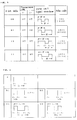
- Fig. 1 shows four kinds of states of two-bit data and the relationships between the four kinds of states and transmission and pulse codes corresponding thereto.
- an input signal composed of plural bit data is divided into words of two-bit data and pulse modulation is carried out for each two-bit data to obtain a pulse unit signal.
- each two-bit data assumes one of four different states and transmission codes (i 1 , j 1 ) which are four kinds of combinations of time intervals 2T and 3T are each assigned to one of the four states.
- the transmission code i 1 represents the time interval between first and third transitions and j 1 the time interval between second and fourth transitions.
- Reference character T denotes a unit time interval, which is equal to the minimum pulse width and the minimum pulse quiescent time of the pulse unit signal.
- the pulse code which forms the pulse unit signal is "1101."
- the time interval between the first and third transitions r 1 and r 3 is determined based on the transmission code i 1 (a).
- the transmission codes i 1 and j 1 are compared and when j 1 ⁇ i 1 , a point in time which is the unit time T behind the first transition r 1 is set as the point of second transition r 2 (b1).
- a point in time which is behind the second transition r 2 by the time corresponding to the transmission code j1 is set as the point of fourth transition r 4 ; thus, a pulse unit signal is obtained which transits its level at these four points in time (c1).
- a point in time which is ahead of the fourth transition r 4 by the time corresponding to the transmission code j 1 is set as the point of second transition r 2 ; thus, a pulse unit signal is obtained which transits its level at these four points in time (c2).
- the two-bit data forming each word is converted into one of four kinds of pulse unit signals each composed of three or four bits.
- the pulse modulating method according to this embodiment will hereinafter be referred to as a two-bit variable length system.
- the pulse unit signals thus converted in word units are concatenated into a sequence of pulse signals.
- the pulse unit signals are concatenated using the last transition (the fourth transition r4 in this embodiment) of the immediately preceding pulse unit signal as the first transition r1 of the immediately following pulse unit signal.
- the pulse unit signals of odd-numbered words rise at the points of first transitions r1 as shown in Figs. 1 and 2
- the pulse unit signals of even-numbered words concatenated with them fall at the points of first transitions r1
- their pulse waveforms are opposite in level to those shown in Figs. 1 and 2 and their pulse codes are also opposite to those shown therein.
- Figs. 5(d) and 6(b) show the waveforms of pulse signals converted using the two-bit variable length system according to the present invention, Fig. 5 showing the waveform with the unit time T (the minimum pulse width of the pulse signal) set at half the data width of the input signal and Fig. 6 the waveform with the unit time T set at a value equal to the data width of the input signal.
- the pulse signal converted by the two bit variable length system is 30-bit pulse signal, and as is evident from Fig. 5, its transmission period is about twice longer than in the case of the NRZ modulation (a) but about half that in the case of the PPM modulation (b) and a little shorter than in the case of the SIR system.
- Fig. 3 is a block diagram illustrating the configuration of pulse modulating equipment 1 according to the present invention, which will be described as being applied to the conversion of the input signal into a pulse signal by the above-described two-bit variable length system.
- a serial input signal composed of plural bit data is input into a serial-parallel converter 3 via a buffer 2.
- the buffer 2 temporarily stores the serial input signal and outputs it as the serial-parallel conversion proceeds in the serial-parallel converter 3.
- the serial-parallel converter 3 converts the serial input signal from the buffer 3 into parallel data in word units of two-bit data for input into an encoder 4.
- the encoder 4 is provided with an encoded table storage circuit 4a wherein the respective states of two-bit data and the pulse codes, such as shown in Fig. 1, are stored in correspondence with each other.
- the pulse codes based on the transmission codes i 1 and j 1 corresponding to the two-bit data, each form a pulse unit signal which has the time interval i 1 between odd-numbered transitions and the time interval j 1 between even-numbered transit positions.
- the encoder 4 reads out the pulse codes corresponding to the two-bit parallel data inputted thereto from the encoded table storage, circuit 4a and provides them to a parallel-serial converter 5 that serves as a pulse signal generator.
- the pulse code of the immediately subsequent even-numbered word is inverted and the falling edge of the preceding pulse unit signal is used as the first transition of the pulse unit signal immediately subsequent thereto.
- Reference numeral 30 denotes a timing generator connected between the output of the encoder 4 and the input of the serial-parallel converter 3, for controlling the output from the serial-parallel converter 3 in accordance with the pulse code output state of the encoder 4. That is, the pulse codes that are output from the encoder 4 are codes of different lengths of three and four bits and when the four-bit pulse code is output, the output timing of the serial-parallel converter 3 is delayed by one bit.
- the parallel-serial converter 5 Based on the pulse codes, the parallel-serial converter 5 generates pulse unit signals and serially applies them to a transmitter circuit 6.
- the transmitter circuit 6 is provided with a pulse output circuit, by which the pulse unit signals output in word units are concatenated into a serial converted pulse signal.
- the transmitter circuit 6 is further provided with an infrared-emitting circuit which emits infrared rays according to the pulse signal; the infrared rays containing the serial converted pulse signal are emitted to pulse demodulating equipment 7.
- Fig. 4 is a block diagram of the pulse demodulating equipment 7 which receives the infrared rays containing the pulse signal and demodulates it into a plurality of bit data.
- the infrared rays containing the pulse signal are subjected to photoelectric conversion and then waveform shaped into a pulse signal.
- the output of the receiver circuit 8 is connected to a rise detector 9 and a fall detector 10 for detecting the rise and fall of the pulse signal which is output from the receiver circuit 8.
- the rise detector 9 Upon detection of the rise of the pulse signal, the rise detector 9 applies the rise detection signal to a first counter 11 connected to the output thereof.
- the first counter 11 always counts clock signals from a clock generator 12 and, when supplied with the rise detection signal, provides the current count value as a first count value UC to a decoder 13, while at the same time it resets its count value to zero and resumes counting the clock signals. That is, the first count value UC from the first counter 11 represents the time interval between two successive rising or leading edges of the pulse signal.
- the fall detector 9 upon detection of the fall of the pulse signal, applies the fall detection signal to a second counter 14 connected to the output thereof.
- the second counter 14 always counts the clock signals from the clock generator 12 as is the case with the first counter 11 and, when supplied with the fall detection signal, provides the current count value as a second count value DC to the decoder 13, while at the same time it resets its count value to zero and resumes counting the clock signals.
- the second count value DC from the second counter 14 represents the time interval between two successive trailing or falling edges of the pulse signal.
- the decoder 13 is provided with a decoded table storage circuit 13a wherein combinations of transmission codes, each composed of the time intervals i 1 and j 1 between the first and third transitions r 1 and r 3 and between the second and fourth transitions r 2 and r 4 , are stored in correspondence with the respective states of the two-bit data.
- the correspondence between the combinations of the transmission codes i 1 and j 1 and the two-bit data in the decoded table storage circuit 13a is the same as the correspondence between the transmission codes i 1 and j 1 and the two-bit data in the encoded table storage circuit 4a of the pulse modulating equipment 1 (see Fig. 1).
- the decoder 13 detects the combination of the transmission codes i 1 and j 1 from the first and second count values UC and DC and reads out the two-bit data corresponding to the detected combination of the transmission codes from the decoded table storage circuit 13a.
- the decoder 13 detects the combination of the transmission codes i 1 and j 1 for each pulse unit signal converted from the two-bit data.
- the pulse unit signal In the case of pulse modulation by the two-bit variable length system, the pulse unit signal have four transitions and the first and fourth transitions are common to the pulse unit signals immediately preceding and succeeding the current one. Accordingly, the pulse signal can be split into pulse unit signals every third transitions.
- the first and second count values UC and DC are alternately input into the decoder 13.
- this point in time is regarded as the time when the pulse unit signals are concatenated and the first and second count values UC and DC input in this period between concatenated points are used to obtain transmission codes i 1 and j 1 of the pulse unit signal of this period.
- the count value input second in the above period represents the time interval between the first and third transitions of the pulse unit signal, that is, the transmission code i 1
- the count value input third in the above period represents the time interval between the second and fourth transitions of the pulse unit signal, that is, the transmission code j 1 .
- the transmission codes i 1 and j 1 are derived from these count values.
- the transmission codes i1 and j1 can be obtained from first and second count values UC1 and DC2, respectively. Assuming that the period of the clock signal from the clock generator 12 is 1/16 the unit time T of the pulse signal, the count value for the unit time T is 16, so that if the first count value UC1 is within 48 ⁇ 3, the transmission code i1 is 3T. Similarly, if the second count value DC2 is within 32 ⁇ 3, the transmission code j1 is 2T.
- the two-bit data corresponding to the combination (3T,2T) of the transmission codes i 1 and j 1 is "1,0," (as shwon in fig. 1) the two-bit data is fed as two-bit parallel data to a parallel-serial converter 15.
- the transmission codes i 1 and j 1 of the second pulse unit signal are derived from the second and first count values DC3 and UC3, respectively. Since the second and first count values DC3 and UC3 are both within 48 ⁇ 3, the transmission codes i 1 and j 1 are (3T,3T), then the corresponding two-bit data "1,1" is readout, and two-bit parallel data "1,1" is fed to the parallel-serial converter 15.
- the parallel-serial converter 15 converts the parallel data, output in units of two bits from the decoder 13, into serial signals and provides them to a buffer 16, which concatenates the serial signals and outputs them as a demodulated signal composed of a plurality of bits.
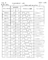
- Fig. 8 is a table explanatory of a pulse modulating method according to another embodiment of the present invention, showing 16 kinds of states of four-bit data and the relationships between them and the transmission codes i 1 ,j 1 and pulse codes corresponding thereto.
- an input signal composed of plural bit data is divided into words of four-bit data, which are each converted into a pulse unit signal of three through five bits according to the state of the four-bit data.
- the pulse modulating method according to this embodiment will hereinafter be called a four-bit variable length system.
- the number of data states of the 4-bit data is 16, 16 combinations of 2T, 2.5T, 3T and 3.5T corresponding to the respective data states are assigned to the transmission codes i 1 and j 1 .
- the transmission codes i 1 and j 1 need not always be integral multiples of the unit time T.
- the corresponding transmission codes i 1 and j 1 are 2.5T and 3T.
- the pulse unit signal that is generated based on such transmission codes has the time interval 2.5T between its first and third transitions r 1 and r 3 and the time interval 2T between its second and fourth transitions r2 and r 4 , and the pulse code for generating the pulse unit signal is "11000111.”
- No description will be given of the method for generating the pulse unit signals based on the transmission codes since it is the same as that described previously with reference to Fig. 2.
- the pulse unit signal is not a rectangular wave composed of integral bits, 1-bit pulse unit signal is represented by a 2-bit pulse code for the sake of convenience.
- the pulse unit signals are concatenated using the fourth transition r4 of the immediately preceding one of them as the first transition of the immediately succeeding pulse unit signal as is the case with the afore-mentioned 2-bit modulating system. Accordingly, the first inversion r1 of the pulse unit signal of an even-numbered word is the fall of the pulse, so that the pulse waveform is opposite in level to that shown in fig. 8 and the pulse code is also opposite.
- Figs. 5(e) and 6(c) show waveforms of the pulse signals converted by the 4-bit variable length system.
- the pulse modulating equipment 1 of Fig. 3 can be used in the 4-bit variable length system, by using an arrangement in which the serial-parallel converter 3 divides the input signal into words of 4-bit data and outputs 4-bit parallel data and the relationships between the bit data and the pulse codes shown in Fig. 8 are stored in the encoded table storage circuit 4a.
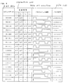
- Fig. 9 is a table explanatory of a pulse modulating method according to further another embodiment of the present invention, showing 16 kinds of states of 4-bit data and the relationships thereto of transmission codes i 1 , i 2 , j 1 , j 2 and pulse codes.
- the input signal composed of plural bit data is divided into words of 4-bit data, each of which is converted into a 6-bit pulse unit signal of fixed length based on the state of the divided 4-bit data.
- the pulse modulating method according to this embodiment will hereinafter be referred to as a 4-bit fixed length system.
- the transmission code i2 represents the time interval between third and fifth transition of the pulse unit signal and the transmission code j2 the time interval between its fourth and sixth transitions.
- the 16 kinds of pulse unit signals are all 6 bits long, and as compared with the above-described variable length system, the number of transitions is six in the case of representing the 4-bit data including the transmission codes i2 and j2.
- NRZ signals which were NRZ-modulated by 6-bit data.
- the transmission codes are gained from the time intervals between leading edges and between trailing edges of the NRZ signals.
- NRZ signals 16 kinds are assumed which were NRZ-modulated by 16 variant kinds of 6-bit data whose most and least significant bits MSB and LSB are "1s" and whose intermediate bits are variant 4-bit data. Since the NRZ signals have their most and least significant bits formed by NRZ modulated versions of bit data "1," the pulse unit signal have rising and trailing edges at their first and sixth bits but each has one of 16 variant kinds of different intermediate waveforms.
- the pulse units signals based on the transmission codes have a fixed 6-bit length.
- the pulse unit signal converted from an even-numbered word has its waveform inverted and is concatenated with the intermediately preceding and succeeding pulse unit signals, using the transitions at the concatenations in common to them.
- Figs. 5(f) and 6(d) show waveforms of pulse signals converted by the 4-bit fixed length system.
- the 4-bit fixed length system permits high-speed transmission as compared with the PPM and SIR systems, and since the pulse unit signals are fixed at 6 bits, demodulation is easier than in the cases of the 2-bit and 4-bit variable length systems of the present invention. Further, even if an error arises in one word during its demodulation, it does not affect the pulse unit signals of other words, and hence it does not constitute an error over the entire demodulation.
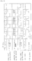
- Figs. 10 and 11 illustrate in block form pulse modulating equipment 17 and pulse demodulating equipment 18 that are used in the 4-bit fixed length system.
- the pulse modulating equipment and the pulse demodulating equipment are substantially identical in construction with those 1 and 7 described previously in respect of Figs. 3 and 4; the same parts are identified by the same reference numerals and no description will be repeated.
- a serial-parallel converter 19 of the pulse modulating equipment 17 divides the serial input signal from the buffer 4 into words of 4-bit data and outputs 4-bit parallel data to an encoder circuit 20.
- the encoder circuit 20 reads out the pulse codes corresponding to the 4-bit parallel data from an encoded table storage circuit 20a having stored therein 4-bit data and pulse codes in correspondence with each other as shown in Fig. 9, the pulse code thus read out being fed to the parallel-serial converter 5.
- This pulse code is to form the pulse unit signal of the waveform shown in Fig. 9 based on the transmission codes i 1 , i 2 , j 1 , j 2 corresponding to the state of the 4-bit data, and since the pulse unit signals have the 6-bit fixed length, the pulse codes that are output are all 6 bits long. Consequently, the timing generator 30 in the pulse modulating equipment 1 of the variable length system is unnecessary.
- the pulse demodulating equipment 18 is provided with a third counter 21 which is supplied with the rise detection signal and the fall detection signal from the rise detector 9 and the fall detector 10.
- the third counter 21 begins to count clock signals at the start of the pulse unit signal and, upon each reception of the rise or fall detection signal, outputs the count value at that time as a third count value BC to a decoder circuit 22, thereby notifying the termination of the pulse unit signal.
- the decoder circuit 22 applies a reset signal to the third counter 21 at the start of the pulse unit signal (that is also the termination of the immediately preceding pulse unit signal) to cause the third counter to start counting the clock signals and, upon each input thereto of the third count value BC for each transition of the pulse signal, compared the third count value BC with the fixed time interval F (corresponding to 6 bits) and, when the third count value BC indicates nearly equal to the time interval of 6 bits, regards the transition at that time as the end of the pulse unit signal. Since the position of termination of the pulse unit signal is also used as the position of start of the immediately succeeding pulse unit signal, the decoder circuit applied the reset signal again to the third counter 21 to cause it to begin counting the clock signals.
- the decoder circuit 22 is provided with a decoded table storage circuit 22a wherein there are stored the transmission codes i 1 , i 2 , j 1 , j 2 and respective states of the 4-bit data in correspondence with each other as shown in Fig. 9.
- the transmission codes are detected from the pulse unit signal divided into each word by the above-described method and the 4-bit data corresponding to the transmission codes is read out from the decoded table storage circuit 22a. Then the 4-bit data is fed as parallel data to the parallel-serial converter 15.
- the decoder circuit 22 makes a comparison between the third count value BC which is output from the third counter 21 upon each transition of the pulse signal and the 6-bit duration.
- the period of the clock signal from the clock generator 12 is 1/16 the unit time or duration T of the pulse signal
- the third count value BC represents the time interval between the start of the pulse unit signal and its transition at the time when the third count value BC is output, and at the end of the pulse unit signal, the pulse unit signal transits its level, so that when the third count value BC is within 96 ⁇ 3, the transition at that time can be regarded as the end of the pulse unit signal.
- one of third count values BC11, BC12 and BC13 are input upon each transition of the pulse signal; since the third count value BC13 is within 96 ⁇ 3, the transition r4 is regarded as the end of the first pulse unit signal.
- third count values BC31, ..., BC34, BC35 are input; since the third count value BC35 is within 96 ⁇ 3, the transition r6 is regarded as the end of the third pulse unit signal.
- the count value input second from the first counter 11 or second counter 14 during the period of each pulse unit signal represents the time interval between first and third transitions, that is, the transmission code i 1 ; similarly, the count value input third represents the transmission code j 1 , the count value input fourth the transmission code i 2 and the count value input fifth the transmission code j 2 .
- the transmission codes i 1 , i 2 , j 1 , j 2 contained in each pulse unit signal are detected from these count values UC and DC.
- the transmission code i 1 is represented by the second count value DC3 and the transmission code j 1 by the first count value UC3, and since the second and first count values DC3 and UC3 are within 64 ⁇ 3 and within 80 ⁇ 3, respectively, the transmission codes i 1 and j 1 of the second pulse unit signal are (4T,5T).
- the transmission codes i 1 , j 1 , i 2 , j 2 of the third pulse unit signal are (3T,3T,2T,2T) since the transmission code i 1 is represented by the first count value UC4, the transmission code j 1 by the second count value DC5, the transmission code i 2 by the first count value UC5 and the transmission code j 2 by the second count value DC6.
- the 4-bit data whose transmission codes i 1 and j 1 correspond to the combination (4t,5T) is "0,0,0,1" as shown in Fig. 9 and this 4-bit data is read out of the decoded table storage circuit 22a and fed as 4-bit parallel data to the parallel-serial converter 15.
- the 4-bit data whose transmission codes i 1 , j 1 , i 2 , j 2 correspond to the combination (3T,3T,2T,2T) is "0,0,1,0” as shown in Fig. 9 and this 4-bit data is read out of the decoded table storage circuit 22a and it is similarly fed as 4-bit parallel data to the parallel serial converter 15.
- each pulse unit signal is used as the first transition of the immediately succeeding pulse unit signal to concatenate the pulse unit signal
- their transitions need not always be used in common.
- an odd-numbered transition can always be defined as the rise of the pulse signal and an even numbered transition as the fall of the pulse signal, so that the transmission codes i and j can be represented by combinations of the time intervals between leading edges and between railing edges of the pulse unit signal.
- the unit time T is used as the minimum pulse width of the pulse unit signal and as the minimum pulse quiescent time, the invention is not limited specifically thereto.
- the frame transmission time for the converted pulse signal can be changed as desired.
- the correspondence between respective states of bit data of each word and the transmission codes are not limited specifically to those shown in the drawings but other correspondence can be used as long as they have a one-to-one correspondence.
- the intermediate 4-bit data of the 6-bit data assumed to obtain combinations of transmission codes are made to correspond to the 4-bit data divided for each word so that they match each other, but the both bit data need not always to match each other.
- the pulse modulating method, pulse modulating equipment and pulse demodulating equipment according to the present invention are suitable for use in optical communication system that employ infrared rays or similar rays of light as carriers.
Abstract
Description
- The present invention relates to a method and equipment for modulating an input signal composed of bit data into a pulse signal, and pulse demodulating equipment.
- There have heretofore been known, as pulse modulating methods of this kind, pulse amplitude modulation (PAM), pulse width modulation (PWM) and pulse phase modulation (PPM) methods which change the pulse amplitude, pulse width and pulse position of the pulse wave used as a carrier, respectively, in accordance with bit data.
- In optical communication systems which use infrared rays and similar rays of light as carriers, the pulse amplitude modulation (PAM) which represents bit data by light intensity, in particular, has a problem with its reliability; therefore, the pulse width modulation (PWM) or pulse phase modulation (PPM) has been used in combination with other modulation methods.
- Figs. 13(a) and (b) show signal waveforms by an ASK (Amplitude-Shift-Keying) system which is an example of such a combined use of different modulation methods. Digital data composed of a plurality of bit data is converted into a pulse signal (a) by an NRZ (Non-Return-to-Zero) modulation scheme which makes the digital data "L" (low) or "H" (high), depending on whether the bit data is "0" or "1" and the pulse signal (a) is used as a modulating wave for ASK modulation of a burst signal into a modulated wave (b).
- In the case of demodulating the modulated wave (b), the envelope waveform of the burst signal is extracted from the input signal and is waveform shaped into the pulse signal (a), from which the plurality of bit data is demodulated by making marking and spacing portions of the pulse signal a "1" and a "0," respectively.
- The ASK system represents 1-bit data by a pulse signal of a waveform of the same duration as that of the data, and hence it permits transmission of data in large quantities and is suitable for high-speed data transmission.
- However, since the pulse width of the pulse signal (a) modulated by the NRZ modulation varies under the influence of frequency characteristics of the light emitting element, the light receiving element and the modem circuit and the transmission line used, the pulse width of the demodulated pulse signal does not always become the same as the pulse width of the modulated signal.
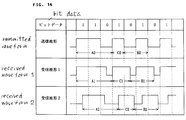
- For example, the received waveform at the demodulating side may sometimes expand its pulse width because of a delay in the fall of the pulse waveform as indicated by a
received waveform 1 in Fig. 14 or narrow its pulse width because of a delay in either of the rise and fall of the pulse waveform as indicated by areceived waveform 2 in Fig. 14. That is, the pulse width C0 of the transmitted waveform does not necessarily become the same as the pulse width C1 or C2 of the receivedwaveforms - In the demodulation of bit data from the pulse signal of such a varied pulse width, a shift in its pulse position causes a demodulation error.
- On the other hand, there has also been known a PPM system which changes the time interval A0 between leading edges of the modulated pulse signal according to the bit data, through utilization of the fact that the time width A0 between leading edges of the pulse signal is equal to the time intervals A1 and A2 between the leading edges of the demodulated signals. As shown in Fig. 13(c), according to the PPM system, each bit data of the digital data is preceded by a pulse of a width T and the subsequent pulse quiescent period is represented by a time interval T or 3T, depending on whether the bit data is "0" or "1" and the thus converted pulse signal (c) is used as a modulating wave for the ASK modulation of the burst signal.
- With the PPM system, demodulation errors decrease, but since each 1-bit data is represented by the pulse quiescent period, the frame transmission period for sending a plurality of bit data in its entirety is long, giving rise to the problem of low transmission rate.
- As a solution to this problem, there has been developed such an SIR modulation system as shown in Fig. 13(d), which represents a plurality of bit data based on the position of respective leading edges of a pulse signal (d) so as to exclude the influence of pulse width variations and raise the transmission rate.
According to the SIR system, a plurality of bit data are divided into words each composed of 2-bit data and the leading edge or phase of a pulse of the width T is changed within atime interval 4T of the 2-bit data in accordance with its four kinds of states. - Even with this pulse modulation method, however, since the bit data is represented by the pulse leading edge alone, the level of redundancy is so high that there is a limit to an increase in the transmission rate.
- The present invention is intended to solve the problems mentioned above and, based on the fact that while in Fig. 14 the pulse width C0 in the received waveform differs from the width in the transmitted waveform, the time intervals A0 and B0 between the pulse leading edges and between the trailing edges remain substantially unchanged, the invention offers a pulse modulation method which represents bit data by the two kinds of time intervals A0, B0, increases the coding efficiency and permits demodulation free from the influence of the transmission system used.
- That is, it is an object of the present invention to provide a pulse modulating method which ensures demodulation of bit data even if the pulse width varies, pulse modulating equipment therefor and pulse demodulating equipment.
- Another object of the present invention is to provide a pulse modulating method which permits high-speed transmission of bit data, pulse modulating equipment therefor and pulse demodulating equipment.
- Another object of the present invention is to provide a pulse modulating method which is low in the level of redundancy and hence is high in coding efficiency and permits high-speed transmission.
- Another object of the present invention is to provide a pulse modulating method which permits reduction of the frame transmission period for the transmission of bit data in its entirety.
- Still another object of the present invention is to provide a pulse modulating method which allows ease in detecting an error during modulation and easy demodulation and, even if a transit signal is applied by noise or the like during demodulation of the current word, prevents it from affecting the demodulation of other words.
- In a pulse modulating method according to an aspect of the present invention which converts an input signal composed of plural bit data into a modulated pulse signal: the input signal is divided into words each composed of n-bit data (n being a positive integer equal to or greater than 2); time intervals im and jm (m being a positive integer starting with 1) are combined to form at least 2n or more transmission codes; all states of the n-bit data are made to correspond to the transmission codes, respectively; in accordance with the transmission code corresponding to the state of the bit data for each word, the input signal is converted into pulse unit signals which have the time interval im between (2m-1)th and (2m+1)th transitions and the time interval jm between (2m)th and (2m+2)th transitions; and the pulse unit signals thus converted in word units are concatenated into a modulated pulse signal.
- With this method, the one of the time intervals im and jm between transitions of the pulse unit signal converted for each word represents the time interval between respective leading edges of the pulse unit signal and the other the time interval between its respective trailing edges. The pulse width of the pulse unit signal varies under the influence of frequency characteristics of the light emitting element, the light receiving element and the modem circuit, but since each rise or fall of the pulse unit signal is affected under the same condition, the pulse signal that represents respective states of the bit data by the time intervals between the leading edges and between the trailing edges can be demodulated without being affected by the above-mentioned frequency characteristics.
- Moreover, since the state of the n-bit data is represented by both of the time intervals between the leading edges and between the trailing edges of the pulse unit signal, redundancy is eliminated and the coding efficiency is increased, permitting high-speed transmission of bit data.
- In a pulse modulating method according to another aspect of the present invention, the first transition of each pulse unit signal is the last transition of the immediately preceding pulse unit signal.
- With this method, the first transition of the pulse unit signal of each word may be a rise or fall of the pulse. That is, the current pulse unit signal can be concatenated with the immediately preceding pulse unit signal, using the last transition of the latter as the first transition of the former, whether it is a rise or fall of the pulse. Since the last transition of the immediately preceding pulse unit signal can be used to concatenate therewith the current pulse unit signal, the frame transmission period for transmitting the entire bit data can be shortened.
- In a pulse modulating method according to another aspect of the present invention, the input signal is divided in units of words each composed of 2-bit data, time intervals i1 and j1 are selected from 2T and 3T, T being a unit time interval, the time intervals i1 and j1 are combined into four different transmission codes, and the input signal is converted into pulse unit signals, each having the time intervals i1 and j1 between first and third transitions and between second and fourth transitions, respectively.
- With this method, the four states of the 2-bit data can be made to correspond to the four transmission codes which are combinations of the
time intervals - In a pulse modulating method according to another aspect of the present invention, the input signal is divided in units of words each composed of 4-bit data, time intervals i1 and j1 are selected from 2T, 2.5T, 3T and 3.5T, T being a unit time interval, the time intervals i1 and j1 are combined into 16 different transmission codes, and the input signal is converted into pulse unit signals, each having the time intervals i1 and j1 between its first and third transitions and between its second and fourth transitions, respectively.
- With this method, 16 kinds of states of the 4-bit data can be made to correspond to the 16 kinds of transmission codes which are combinations of 2T, 2.5T, 3T and 3.5T. The time intervals i1 and j1 between the first and third transitions of the pulse unit signal and between its second and fourth transitions are any one of 2T, 2.5T, 3T and 3.5T, and letting the pulse width be represented by T, the duration of each pulse unit signal is in the range of 3T to 4.5T. Thus, the period for transmitting all of the bit data in the can be reduced.
- According to another aspect of the present invention, the unit time interval T is the data width of 1-bit data.
- According to another aspect of the present invention, the time interval F between first and last transitions of each pulse unit signal is constant.
- With this method, since the duration F of each pulse unit signal is constant, the period for transmitting all of the bit data is also constant, allowing ease in detecting a demodulation error. Further, since the modulated signal can be demodulated into bit data of each word at the time intervals F, the demodulation is easy and, even if a transit signal is applied by noise or the like, it does not affect the demodulation of other words.
- In a pulse modulating method according to another aspect of the present invention, 2n kinds of NRZ signals are assumed which were NRZ modulated by (n+2) pieces of bit data whose most and least significant bits are "1s" in common to them but whose intermediate bits differ from one another, and time intervals between (2m-1)th and (2m+1)th transitions and between its (2m)th and (2m+2)th transitions of each NRZ signal are combinations of the time intervals im and jm and the time interval F is used as the duration of NRZ signal which were NRZ modulated by (n+2) pieces of bit data.
- With this method, the 2n kinds of NRZ signals are pulse signals that correspond to all different data of the intermediate n-bit data. The NRZ signals have the time interval between transitions at their opposite ends defined by the time interval of the (n+2) bit data but differ in the intermediate pulse waveform and in the combination of time intervals between their odd-numbered transitions and between their even-numbered transitions. Hence, by defining the combinations of these time intervals by the combinations of the time intervals im and jm, it is possible to obtain 2n kinds of transmission codes which provide pulse unit signals of the fixed duration F.
- Pulse modulating equipment according to another aspect of the present invention comprises: a serial-parallel converter which divides a serial input signal composed of a plurality of bit data in steps of n bits (n being a positive integer equal to or greater than 2) and outputs the input signal as n-bit parallel data; an encoded table storage circuit which obtains at least 2n kinds of different transmission codes by combining time intervals im and jm (m being a positive integer beginning with 1) and wherein pulse codes which has time intervals between (2m-1)th and (2m+1)th transitions and between (2m)th and (2m+2)th transitions of pulse unit signals defined by im and jm, respectively, in accordance with the transmission codes are stored in correspondence with respective states of n-bit parallel data; an encoder circuit which reads out the pulse code corresponding to the n-bit parallel data from the encoded table storage circuit and outputs it; a pulse signal generator which generates pulse unit signals from the pulse codes and outputs them serially; and a pulse output circuit which concatenates the pulse unit signals converted every n-bit parallel data into a pulse signal and outputs it.
- With this construction, a plurality of bit data are divided by the serial-parallel converter into n-bit parallel data. The encoder circuit supplies the pulse signal generator with pulse codes corresponding to the states of n-bit parallel data. Based on the pulse codes, the pulse signal generator serially outputs pulse unit signals which has the time intervals between odd-numbered transitions and between even-numbered transitions defined as im and jm, respectively. The pulse output circuit outputs the pulse signal into which the pulse unit signals are concatenated.
- Hence, the bit data of the n-bit parallel data is represented by the time intervals between trailing edges of the pulse unit signal and between its leading edges, and even if the pulse width changes under the influence of the state of transmission, it is possible to output a pulse signal free from a demodulation error.
- Pulse demodulating equipment according to another aspect of the present invention comprises: a transition detecting circuit which divides an input pulse signal every fixed number K of transitions and, for each pulse unit signal defined by the K transitions, repeatedly detects the time intervals im and jm between the (2m-1)th (m being a positive integer beginning with 1) and (2m+1)th transitions and between the (2m)th and (2m+2)th transitions; a decoded table storage circuit wherein at least 2n (n being a positive integer equal to or greater than 2) different combinations of time intervals im and jm (m being a positive integer in the range of 1 to k) are stored in correspondence with respective states of the n-bit data; a decoder circuit which reads out the n-bit data from the decoded table storage circuit corresponding to the combination of the time intervals im and jm detected by the transition detecting circuit and outputs it as n-bit parallel data; and a parallel-serial converter which converts each n-bit parallel data demodulated for each pulse unit signal into a serial signal and outputs it as a signal composed of a plurality of bit data.
- With this construction, the input pulse signal is divided every fixed number K of transitions. By setting the number K to be equal to the number of inversions of the pulse unit signal converted from the n-bit data, the input pulse signal is divided into pulse unit signals. The transition detecting circuit detects, for each pulse unit signal, the time intervals im and jm between its odd-numbered transitions and between its even-numbered transitions.
- The decoder circuit reads out the n-bit data from the decoded table storage circuit corresponding to the combination of the time intervals im and jm and outputs it as n-bit parallel data. The n-bit parallel data are converted by the parallel-serial converter into a serial signal of n-bit data, which is concatenated with a serial signal of n-bit data similarly demodulated from the immediately preceding pulse unit signal, obtaining an output signal composed of plural bit data.
- Hence, bit data can be demodulated from the pulse signal representing the plural bit data by the time intervals between the trailing edges and between leading edges, and even if the pulse width changes under the influence of the state of transmission, no demodulation error will arise.
- Moreover, even if the pulse unit signals converted from the n-bit data have different durations, it is possible to divide the input pulse signal into pulse unit signals by adjusting the number K of transitions and demodulate the pulse signal for each pulse unit signal.
- Pulse demodulating equipment according to another aspect of the present invention comprises: a transition detecting circuit which divides an input pulse signal at fixed time intervals F and, for each pulse unit signal defined by the duration F, detects time intervals im and jm between (2m-1)th (m being a positive integer beginning with 1) and (2m+1)th transitions and between (2m)th and (2m+2)th transitions; a decoded table storage circuit wherein at least 2n (n being a positive integer equal to or greater than 2) different combinations of time intervals im and jm (m being a positive integer in the range of 1 to k) are stored in correspondence with respective states of the n-bit data; a decoder circuit which reads out the n-bit data from the decoded table storage circuit corresponding to the combination of the time intervals im and jm detected by the transition detecting circuit and outputs it as n-bit parallel data; and a parallel-serial converter which converts each n-bit parallel data demodulated for each pulse unit signal into a serial signal and outputs it as a signal composed of a plurality of bit data.
- With this construction, the input pulse signal is divided at fixed time intervals F. By setting the duration F to be equal to the duration of each pulse unit signal converted from the n-bit data, the input pulse signal is divided into pulse unit signals. The transition detecting circuit detects, for each pulse unit signal, the time intervals im and jm between its odd-numbered transitions and between its even-numbered transitions. The decoder circuit reads out the n-bit data from the decoded table storage circuit corresponding to the combination of the time intervals im and jm and outputs it as n-bit parallel data. The n-bit parallel data are converted by the parallel-serial converter into a serial signal of n-bit data, which is concatenated with a serial signal of n-bit data similarly demodulated from the immediately preceding pulse unit signal, obtaining an output signal composed of plural bit data.
- Hence, bit data can be demodulated from the pulse signal representing the plural bit data by the time intervals between the trailing edges and between leading edges, and even if the pulse width changes under the influence of the state of transmission, no demodulation error will arise.
-
- Fig. 1 is an explanatory diagram showing four kinds of states of 2-bit data and the relationships thereto of transmission codes and pulse codes in a 2-bit variable length system according to a first embodiment of the present invention; and Fig. 2 is an explanatory diagram showing the procedure for generating pulse unit signals in accordance weth following the transmission codes;
- Fig. 3 is a block diagram illustrating the configuration of
pulse modulating equipment 1 for use in the 2-bit variable length system according to the present invention; and Fig. 4 is a block diagram illustrating pulse demodulating equipment for demodulating plural bit data from a pulse signal converted by the 2-bit variable length system according to the present invention; - Fig. 5 is a waveform diagram showing, in comparison, a pulse signal converted by a conventional pulse modulating method and a pulse signal converted by the pulse modulating method according to the present invention, with the minimum width T of each pulse signal set at 1/2 the data width of the input signal; and Fig. 6 is a waveform diagram showing, in comparison, a pulse signal converted by a conventional pulse modulating method and a pulse signal converted by the pulse modulating method according to the present invention, with the minimum width T of each pulse signal set to be equal to the data width of the input signal;
- Fig. 7 is a diagram for explaining processing in a
decoder circuit 13; - Fig. 8 is an explanatory diagram showing 16 kinds of states of 4-bit data and the relationships thereto of transmission codes and pulse codes in a 4-bit variable length system according to a second embodiment of the present invention; and Fig. 9 is an explanatory diagram showing 16 kinds of states of 4-bit data and the relationships thereto of transmission codes and pulse codes in a 4-bit fixed length system according to a third embodiment of the present invention;
- Fig. 10 is a block diagram illustrating the configuration of
pulse modulating equipment 17 for use in the 4-bit fixed length system according to the present invention; and Fig. 11 is a block diagram illustrating the configuration of pulse demodulating equipment 18 for use in the 4-bit fixed length system according to the present invention; - Fig. 13 is a diagram for explaining processing in a
decoder circuit 22; - Fig. 13 is a waveform diagram showing a conventional pulse modulating method; and Fig. 14 is a waveform diagram showing the relationships between transmitted and received waveforms.
- A description will be given, with reference to Figs. 1 through 6, of a pulse modulating method according to a first embodiment of the present invention.
- Fig. 1 shows four kinds of states of two-bit data and the relationships between the four kinds of states and transmission and pulse codes corresponding thereto.
- In this embodiment, an input signal composed of plural bit data is divided into words of two-bit data and pulse modulation is carried out for each two-bit data to obtain a pulse unit signal.
- As depicted in Fig. 1, each two-bit data assumes one of four different states and transmission codes (i1, j1) which are four kinds of combinations of
time intervals - The transmission code i1 represents the time interval between first and third transitions and j1 the time interval between second and fourth transitions. Reference character T denotes a unit time interval, which is equal to the minimum pulse width and the minimum pulse quiescent time of the pulse unit signal.
- Accordingly, when the two-bit data of one word is, for example, "1,0," the time intervals between the first and third transitions r1 and r3 and between the second and fourth transitions r2 and r4 are 3T and 2T, respectively, and the minimum pulse width and the minimum pulse quiescent time are T as shown in Fig. 1; thus, the pulse code which forms the pulse unit signal is "1101."
- Referring now to Fig. 2, the procedure for forming the pulse unit signal based on the transmission codes will be described.
- In the first place, the time interval between the first and third transitions r1 and r3 is determined based on the transmission code i1 (a).
- Next, the transmission codes i1 and j1 are compared and when j1 ≧ i1, a point in time which is the unit time T behind the first transition r1 is set as the point of second transition r2 (b1).
- Then, a point in time which is behind the second transition r2 by the time corresponding to the transmission code j1 is set as the point of fourth transition r4; thus, a pulse unit signal is obtained which transits its level at these four points in time (c1).
- On the other hand, when j1<i1, a point in time which is the unit time T behind the third transition r3 is set as the point of fourth transition r4 (b2).
- Following this, a point in time which is ahead of the fourth transition r4 by the time corresponding to the transmission code j1 is set as the point of second transition r2; thus, a pulse unit signal is obtained which transits its level at these four points in time (c2).
- In this way, the two-bit data forming each word is converted into one of four kinds of pulse unit signals each composed of three or four bits. (The pulse modulating method according to this embodiment will hereinafter be referred to as a two-bit variable length system.)
- Incidentally, the pulse unit signals thus converted in word units are concatenated into a sequence of pulse signals. In this instance, the pulse unit signals are concatenated using the last transition (the fourth transition r4 in this embodiment) of the immediately preceding pulse unit signal as the first transition r1 of the immediately following pulse unit signal. Hence, the pulse unit signals of odd-numbered words rise at the points of first transitions r1 as shown in Figs. 1 and 2, whereas the pulse unit signals of even-numbered words concatenated with them fall at the points of first transitions r1, and consequently, their pulse waveforms are opposite in level to those shown in Figs. 1 and 2 and their pulse codes are also opposite to those shown therein.
- Figs. 5(d) and 6(b) show the waveforms of pulse signals converted using the two-bit variable length system according to the present invention, Fig. 5 showing the waveform with the unit time T (the minimum pulse width of the pulse signal) set at half the data width of the input signal and Fig. 6 the waveform with the unit time T set at a value equal to the data width of the input signal.
- Assuming that the input signal is 16-bit data such as shown in Figs. 5 and 6, the pulse signal converted by the two bit variable length system is 30-bit pulse signal, and as is evident from Fig. 5, its transmission period is about twice longer than in the case of the NRZ modulation (a) but about half that in the case of the PPM modulation (b) and a little shorter than in the case of the SIR system.
- Fig. 3 is a block diagram illustrating the configuration of
pulse modulating equipment 1 according to the present invention, which will be described as being applied to the conversion of the input signal into a pulse signal by the above-described two-bit variable length system. - In Fig. 3, a serial input signal composed of plural bit data is input into a serial-
parallel converter 3 via abuffer 2. Thebuffer 2 temporarily stores the serial input signal and outputs it as the serial-parallel conversion proceeds in the serial-parallel converter 3. The serial-parallel converter 3 converts the serial input signal from thebuffer 3 into parallel data in word units of two-bit data for input into anencoder 4. - The
encoder 4 is provided with an encodedtable storage circuit 4a wherein the respective states of two-bit data and the pulse codes, such as shown in Fig. 1, are stored in correspondence with each other. As described previously, the pulse codes, based on the transmission codes i1 and j1 corresponding to the two-bit data, each form a pulse unit signal which has the time interval i1 between odd-numbered transitions and the time interval j1 between even-numbered transit positions. - The
encoder 4 reads out the pulse codes corresponding to the two-bit parallel data inputted thereto from the encoded table storage,circuit 4a and provides them to a parallel-serial converter 5 that serves as a pulse signal generator. - For example, if the two-bit parallel data is "0,1," a pulse code of four bits "1011" is output.
- In this instance, if the least significant bit LSB of the immediately preceding pulse code is "1," the above pulse code is inverted to "0100." The reason for this is that since the least significant bit LSB of the pulse code of the odd-numbered word is a "1" to form the last transition r4 of the pulse unit signal as a falling edge, the pulse code of the immediately subsequent even-numbered word is inverted and the falling edge of the preceding pulse unit signal is used as the first transition of the pulse unit signal immediately subsequent thereto.
-
Reference numeral 30 denotes a timing generator connected between the output of theencoder 4 and the input of the serial-parallel converter 3, for controlling the output from the serial-parallel converter 3 in accordance with the pulse code output state of theencoder 4. That is, the pulse codes that are output from theencoder 4 are codes of different lengths of three and four bits and when the four-bit pulse code is output, the output timing of the serial-parallel converter 3 is delayed by one bit. - Based on the pulse codes, the parallel-
serial converter 5 generates pulse unit signals and serially applies them to atransmitter circuit 6. Thetransmitter circuit 6 is provided with a pulse output circuit, by which the pulse unit signals output in word units are concatenated into a serial converted pulse signal. Thetransmitter circuit 6 is further provided with an infrared-emitting circuit which emits infrared rays according to the pulse signal; the infrared rays containing the serial converted pulse signal are emitted topulse demodulating equipment 7. - Fig. 4 is a block diagram of the
pulse demodulating equipment 7 which receives the infrared rays containing the pulse signal and demodulates it into a plurality of bit data. - When received by a
receiver circuit 8, the infrared rays containing the pulse signal are subjected to photoelectric conversion and then waveform shaped into a pulse signal. The output of thereceiver circuit 8 is connected to arise detector 9 and afall detector 10 for detecting the rise and fall of the pulse signal which is output from thereceiver circuit 8. - Upon detection of the rise of the pulse signal, the
rise detector 9 applies the rise detection signal to afirst counter 11 connected to the output thereof. - The
first counter 11 always counts clock signals from aclock generator 12 and, when supplied with the rise detection signal, provides the current count value as a first count value UC to adecoder 13, while at the same time it resets its count value to zero and resumes counting the clock signals. That is, the first count value UC from thefirst counter 11 represents the time interval between two successive rising or leading edges of the pulse signal. - On the other hand, upon detection of the fall of the pulse signal, the
fall detector 9 applies the fall detection signal to asecond counter 14 connected to the output thereof. - The
second counter 14 always counts the clock signals from theclock generator 12 as is the case with thefirst counter 11 and, when supplied with the fall detection signal, provides the current count value as a second count value DC to thedecoder 13, while at the same time it resets its count value to zero and resumes counting the clock signals. The second count value DC from thesecond counter 14 represents the time interval between two successive trailing or falling edges of the pulse signal. - The
decoder 13 is provided with a decoded table storage circuit 13a wherein combinations of transmission codes, each composed of the time intervals i1 and j1 between the first and third transitions r1 and r3 and between the second and fourth transitions r2 and r4, are stored in correspondence with the respective states of the two-bit data. The correspondence between the combinations of the transmission codes i1 and j1 and the two-bit data in the decoded table storage circuit 13a is the same as the correspondence between the transmission codes i1 and j1 and the two-bit data in the encodedtable storage circuit 4a of the pulse modulating equipment 1 (see Fig. 1). - The
decoder 13 detects the combination of the transmission codes i1 and j1 from the first and second count values UC and DC and reads out the two-bit data corresponding to the detected combination of the transmission codes from the decoded table storage circuit 13a. - Turning to Fig 7, the processing in the
decoder 13 will be described below. - Provided that the pulse signal fed thereto from the
receiver circuit 8 is a pulse signal of such a waveform as shown in Fig. 7, thedecoder 13 detects the combination of the transmission codes i1 and j1 for each pulse unit signal converted from the two-bit data. In the case of pulse modulation by the two-bit variable length system, the pulse unit signal have four transitions and the first and fourth transitions are common to the pulse unit signals immediately preceding and succeeding the current one. Accordingly, the pulse signal can be split into pulse unit signals every third transitions. - As depicted in Fig. 7, upon each detection of the rise and fall of the pulse signal, the first and second count values UC and DC are alternately input into the
decoder 13. Hence, whenever the first and second count values UC and DC are input into the decoder a total of three times, this point in time is regarded as the time when the pulse unit signals are concatenated and the first and second count values UC and DC input in this period between concatenated points are used to obtain transmission codes i1 and j1 of the pulse unit signal of this period. - As will be seen from Fig. 7, the count value input second in the above period represents the time interval between the first and third transitions of the pulse unit signal, that is, the transmission code i1, and the count value input third in the above period represents the time interval between the second and fourth transitions of the pulse unit signal, that is, the transmission code j1. In this way, the transmission codes i1 and j1 are derived from these count values.
- In the case of a first pulse unit signal, the transmission codes i1 and j1 can be obtained from first and second count values UC1 and DC2, respectively. Assuming that the period of the clock signal from the
clock generator 12 is 1/16 the unit time T of the pulse signal, the count value for the unit time T is 16, so that if the first count value UC1 is within 48 ± 3, the transmission code i1 is 3T. Similarly, if the second count value DC2 is within 32 ± 3, the transmission code j1 is 2T. - Since the two-bit data corresponding to the combination (3T,2T) of the transmission codes i1 and j1 is "1,0," (as shwon in fig. 1) the two-bit data is fed as two-bit parallel data to a parallel-
serial converter 15. - Likewise, the transmission codes i1 and j1 of the second pulse unit signal are derived from the second and first count values DC3 and UC3, respectively. Since the second and first count values DC3 and UC3 are both within 48 ± 3, the transmission codes i1 and j1 are (3T,3T), then the corresponding two-bit data "1,1" is readout, and two-bit parallel data "1,1" is fed to the parallel-
serial converter 15. - The parallel-
serial converter 15 converts the parallel data, output in units of two bits from thedecoder 13, into serial signals and provides them to abuffer 16, which concatenates the serial signals and outputs them as a demodulated signal composed of a plurality of bits. - As described above, the
pulse demodulating equipment 7 detects the time intervals between the leading or rising edges of the pulse signal and between its trailing or falling edges and demodulates the pulse signal into bit data. Hence, even if the pulse width changes under the influence of the transmission line or the frequency characteristics in the modem, the time intervals will not change and the demodulation can be achieved with accuracy. - Fig. 8 is a table explanatory of a pulse modulating method according to another embodiment of the present invention, showing 16 kinds of states of four-bit data and the relationships between them and the transmission codes i1,j1 and pulse codes corresponding thereto.
- In this embodiment, an input signal composed of plural bit data is divided into words of four-bit data, which are each converted into a pulse unit signal of three through five bits according to the state of the four-bit data. (The pulse modulating method according to this embodiment will hereinafter be called a four-bit variable length system.)
- As shown in Fig. 8, the number of data states of the 4-bit data is 16, 16 combinations of 2T, 2.5T, 3T and 3.5T corresponding to the respective data states are assigned to the transmission codes i1 and j1. When the unit time T is used as the minimum pulse width of the pulse unit signal and the minimum pulse quiescent time as mentioned above, the transmission codes i1 and j1 need not always be integral multiples of the unit time T.
- For example, in case a 4-bit data divided into word is "1,0,0,1", the corresponding transmission codes i1 and j1 are 2.5T and 3T. The pulse unit signal that is generated based on such transmission codes has the time interval 2.5T between its first and third transitions r1 and r3 and the
time interval 2T between its second and fourth transitions r2 and r4, and the pulse code for generating the pulse unit signal is "11000111." No description will be given of the method for generating the pulse unit signals based on the transmission codes since it is the same as that described previously with reference to Fig. 2. Incidentally, since the pulse unit signal is not a rectangular wave composed of integral bits, 1-bit pulse unit signal is represented by a 2-bit pulse code for the sake of convenience. - Also in this instance, the pulse unit signals are concatenated using the fourth transition r4 of the immediately preceding one of them as the first transition of the immediately succeeding pulse unit signal as is the case with the afore-mentioned 2-bit modulating system. Accordingly, the first inversion r1 of the pulse unit signal of an even-numbered word is the fall of the pulse, so that the pulse waveform is opposite in level to that shown in fig. 8 and the pulse code is also opposite.
- Since the pulse unit signals are concatenated using the last inversion of the immediately preceding signal as the first inversion of the succeeding signal as mentioned above, the frame transmission period for transmitting the whole bit data can be reduced.
- Figs. 5(e) and 6(c) show waveforms of the pulse signals converted by the 4-bit variable length system.
- As will be seen from Figs. 5(e) and 6(c), the frame transmission period for transmitting the whole bit data is half that in the case of the 2-bit variable length system, substantially equal to that in the case of the NRZ modulating system and extremely shorter than in the cases of the PPM and SIR systems. By dividing the input signal into data of a larger number of bits in the pulse modulation, the entire transmission period can be further reduced.
- The
pulse modulating equipment 1 of Fig. 3 can be used in the 4-bit variable length system, by using an arrangement in which the serial-parallel converter 3 divides the input signal into words of 4-bit data and outputs 4-bit parallel data and the relationships between the bit data and the pulse codes shown in Fig. 8 are stored in the encodedtable storage circuit 4a. - Further, the
pulse demodulating equipment 7 of Fig. 4 can be used by storing in its decoded table storage circuit 13a the relationships between the bit data and the pulse codes shown in Fig. 8. - Fig. 9 is a table explanatory of a pulse modulating method according to further another embodiment of the present invention, showing 16 kinds of states of 4-bit data and the relationships thereto of transmission codes i1, i2, j1, j2 and pulse codes.
- In this third embodiment, the input signal composed of plural bit data is divided into words of 4-bit data, each of which is converted into a 6-bit pulse unit signal of fixed length based on the state of the divided 4-bit data. (The pulse modulating method according to this embodiment will hereinafter be referred to as a 4-bit fixed length system.)
- The transmission code i2 represents the time interval between third and fifth transition of the pulse unit signal and the transmission code j2 the time interval between its fourth and sixth transitions. As shown, the 16 kinds of pulse unit signals are all 6 bits long, and as compared with the above-described variable length system, the number of transitions is six in the case of representing the 4-bit data including the transmission codes i2 and j2.
- To obtain 16 variant kinds of transmission codes, in accordance with which pulse unit signals of fixed 6-bit length, NRZ signals are assumed which were NRZ-modulated by 6-bit data. The transmission codes are gained from the time intervals between leading edges and between trailing edges of the NRZ signals.
- That is, 16 kinds of NRZ signals are assumed which were NRZ-modulated by 16 variant kinds of 6-bit data whose most and least significant bits MSB and LSB are "1s" and whose intermediate bits are variant 4-bit data. Since the NRZ signals have their most and least significant bits formed by NRZ modulated versions of bit data "1," the pulse unit signal have rising and trailing edges at their first and sixth bits but each has one of 16 variant kinds of different intermediate waveforms.
- Hence, by deriving the transmission codes i1, i2, j1, j2 from the time intervals between odd-numbered transitions and between even-numbered transitions, 16 kinds of combinations are obtained and the pulse units signals based on the transmission codes have a fixed 6-bit length.
- Also in this 4-bit fixed length system, the pulse unit signal converted from an even-numbered word has its waveform inverted and is concatenated with the intermediately preceding and succeeding pulse unit signals, using the transitions at the concatenations in common to them.
- Figs. 5(f) and 6(d) show waveforms of pulse signals converted by the 4-bit fixed length system.
- As is evident from Fig. 6, the 4-bit fixed length system permits high-speed transmission as compared with the PPM and SIR systems, and since the pulse unit signals are fixed at 6 bits, demodulation is easier than in the cases of the 2-bit and 4-bit variable length systems of the present invention. Further, even if an error arises in one word during its demodulation, it does not affect the pulse unit signals of other words, and hence it does not constitute an error over the entire demodulation.
- Figs. 10 and 11 illustrate in block form
pulse modulating equipment 17 and pulse demodulating equipment 18 that are used in the 4-bit fixed length system. - The pulse modulating equipment and the pulse demodulating equipment are substantially identical in construction with those 1 and 7 described previously in respect of Figs. 3 and 4; the same parts are identified by the same reference numerals and no description will be repeated.
- A serial-
parallel converter 19 of thepulse modulating equipment 17 divides the serial input signal from thebuffer 4 into words of 4-bit data and outputs 4-bit parallel data to an encoder circuit 20. - The encoder circuit 20 reads out the pulse codes corresponding to the 4-bit parallel data from an encoded table storage circuit 20a having stored therein 4-bit data and pulse codes in correspondence with each other as shown in Fig. 9, the pulse code thus read out being fed to the parallel-
serial converter 5. - This pulse code is to form the pulse unit signal of the waveform shown in Fig. 9 based on the transmission codes i1, i2, j1, j2 corresponding to the state of the 4-bit data, and since the pulse unit signals have the 6-bit fixed length, the pulse codes that are output are all 6 bits long. Consequently, the
timing generator 30 in thepulse modulating equipment 1 of the variable length system is unnecessary. - The pulse demodulating equipment 18 is provided with a
third counter 21 which is supplied with the rise detection signal and the fall detection signal from therise detector 9 and thefall detector 10. In order that thedecoder circuit 22 divides the input pulse signal at regular time intervals F (the time intervals corresponding 6-bit data in the case of the 4-bit fixed length system) for the demodulation of each pulse unit signal, thethird counter 21 begins to count clock signals at the start of the pulse unit signal and, upon each reception of the rise or fall detection signal, outputs the count value at that time as a third count value BC to adecoder circuit 22, thereby notifying the termination of the pulse unit signal. - That is, the
decoder circuit 22 applies a reset signal to thethird counter 21 at the start of the pulse unit signal (that is also the termination of the immediately preceding pulse unit signal) to cause the third counter to start counting the clock signals and, upon each input thereto of the third count value BC for each transition of the pulse signal, compared the third count value BC with the fixed time interval F (corresponding to 6 bits) and, when the third count value BC indicates nearly equal to the time interval of 6 bits, regards the transition at that time as the end of the pulse unit signal. Since the position of termination of the pulse unit signal is also used as the position of start of the immediately succeeding pulse unit signal, the decoder circuit applied the reset signal again to thethird counter 21 to cause it to begin counting the clock signals. - The
decoder circuit 22 is provided with a decoded table storage circuit 22a wherein there are stored the transmission codes i1, i2, j1, j2 and respective states of the 4-bit data in correspondence with each other as shown in Fig. 9. The transmission codes are detected from the pulse unit signal divided into each word by the above-described method and the 4-bit data corresponding to the transmission codes is read out from the decoded table storage circuit 22a. Then the 4-bit data is fed as parallel data to the parallel-serial converter 15. - Turning to Fig. 12, the above processing in the
decoder circuit 22 will be described below. - Assuming that the pulse signal from the
receiver circuit 8 has such a waveform as shown in Fig. 12, thedecoder circuit 22 makes a comparison between the third count value BC which is output from thethird counter 21 upon each transition of the pulse signal and the 6-bit duration. Provided that the period of the clock signal from theclock generator 12 is 1/16 the unit time or duration T of the pulse signal, the pulse unit signal whose 1-bit duration is equal to the unit time T indicates that the count value is 616=96 and has reached the end of the pulse unit signal. On the other hand, the third count value BC represents the time interval between the start of the pulse unit signal and its transition at the time when the third count value BC is output, and at the end of the pulse unit signal, the pulse unit signal transits its level, so that when the third count value BC is within 96 ± 3, the transition at that time can be regarded as the end of the pulse unit signal.
- For example, during the input of the first pulse unit signal, one of third count values BC11, BC12 and BC13 are input upon each transition of the pulse signal; since the third count value BC13 is within 96 ± 3, the transition r4 is regarded as the end of the first pulse unit signal. Similarly, during the input of the third pulse unit signal, third count values BC31, ..., BC34, BC35 are input; since the third count value BC35 is within 96 ± 3, the transition r6 is regarded as the end of the third pulse unit signal.
- As is evident from Fig. 12, the count value input second from the
first counter 11 orsecond counter 14 during the period of each pulse unit signal represents the time interval between first and third transitions, that is, the transmission code i1; similarly, the count value input third represents the transmission code j1, the count value input fourth the transmission code i2 and the count value input fifth the transmission code j2. - Thus, the transmission codes i1, i2, j1, j2 contained in each pulse unit signal are detected from these count values UC and DC.
- For example, in the second pulse unit signal, the transmission code i1 is represented by the second count value DC3 and the transmission code j1 by the first count value UC3, and since the second and first count values DC3 and UC3 are within 64 ± 3 and within 80 ± 3, respectively, the transmission codes i1 and j1 of the second pulse unit signal are (4T,5T). Likewise, the transmission codes i1, j1, i2, j2 of the third pulse unit signal are (3T,3T,2T,2T) since the transmission code i1 is represented by the first count value UC4, the transmission code j1 by the second count value DC5, the transmission code i2 by the first count value UC5 and the transmission code j2 by the second count value DC6.
- The 4-bit data whose transmission codes i1 and j1 correspond to the combination (4t,5T) is "0,0,0,1" as shown in Fig. 9 and this 4-bit data is read out of the decoded table storage circuit 22a and fed as 4-bit parallel data to the parallel-
serial converter 15. The 4-bit data whose transmission codes i1, j1, i2, j2 correspond to the combination (3T,3T,2T,2T) is "0,0,1,0" as shown in Fig. 9 and this 4-bit data is read out of the decoded table storage circuit 22a and it is similarly fed as 4-bit parallel data to the parallelserial converter 15. - While in the embodiments of the present invention described above the last transition of each pulse unit signal is used as the first transition of the immediately succeeding pulse unit signal to concatenate the pulse unit signal, their transitions need not always be used in common. In such a case, an odd-numbered transition can always be defined as the rise of the pulse signal and an even numbered transition as the fall of the pulse signal, so that the transmission codes i and j can be represented by combinations of the time intervals between leading edges and between railing edges of the pulse unit signal.
- Furthermore, although in the embodiments of the invention the unit time T is used as the minimum pulse width of the pulse unit signal and as the minimum pulse quiescent time, the invention is not limited specifically thereto. By changing the unit time T, the frame transmission time for the converted pulse signal can be changed as desired.
- The correspondence between respective states of bit data of each word and the transmission codes are not limited specifically to those shown in the drawings but other correspondence can be used as long as they have a one-to-one correspondence. In the third embodiment, in particular, the intermediate 4-bit data of the 6-bit data assumed to obtain combinations of transmission codes are made to correspond to the 4-bit data divided for each word so that they match each other, but the both bit data need not always to match each other.
- As described above, the pulse modulating method, pulse modulating equipment and pulse demodulating equipment according to the present invention are suitable for use in optical communication system that employ infrared rays or similar rays of light as carriers.
Claims (11)
- A pulse modulating method which converts an input signal composed of plural bit data into a modulated pulse signal, characterized in:that the input signal is divided into words each composed of n-bit data (n being a positive integer equal to or greater than 2);that time intervals im and jm (m being a positive integer starting with 1) are combined to form at least 2n or more different transmission codes;that all states of the n-bit data are made to correspond to the transmission codes, respectively;that, in accordance with the transmission code corresponding to the state of the bit data for each word, the input signal is converted into pulse unit signals which have the time interval im between (2m-1)th and (2m+1)th transitions and the time interval jm between (2m)th and (2m+2)th transitions; andthat the pulse unit signals thus converted in word units are concatenated into a modulated pulse signal.
- A pulse modulating method as claimed in claim 1, characterized in that a first transition of each pulse unit signal is the last transition of the immediately preceding pulse unit signal.
- A pulse modulating method as claimed in claim 1 or 2, characterized in:that the input signal is divided in units of words each composed of 2-bit data;that time intervals i1 and j1 are selected from 2T and 3T, T being a unit time interval;that the time intervals i1 and j1 are combined into four different kinds of transmission codes; andThat the input signal is converted into pulse unit signals, each having the time intervals i1 and j1 between first and third transitions and between second and fourth transitions, respectively.
- A pulse modulating method as claimed in claim 3, characterized in that the unit time interval T is the data width of 1-bit data.
- A pulse modulating method as claimed in claim 1 or 2, characterized in:that the input signal is divided in units of words each composed of 4-bit data;that time intervals i1 and j1 are selected from 2T, 2.5T, 3T and 3.5T, T being a unit time interval;that the time intervals i1 and j1 are combined into 16 different kinds of transmission codes; andthat the input signal is converted into pulse unit signals, each having the time intervals i1 and j1 between its first and third transitions and between its second and fourth transitions, respectively.
- A pulse modulating method as claimed in claim 5, characterized in that the unit time interval T is the data width of 1-bit data.
- A pulse modulating method as claimed in claim 1 or 2, characterized in that the time intervals F between the first and last transitions of the pulse unit signals are constant.
- A pulse modulating method as claimed in claim 7, characterized in:that 2n kinds of NRZ signals are assumed which were NRZ modulated by (n+2) pieces of bit data whose most and least significant bits are "1s" in common to them but whose intermediate bit data differ from one another;that time intervals between (2m-1)th and (2m+1)th transitions and between its (2m)th and (2m+2)th transitions of each NRZ signal are combinations of the time intervals im and jm ; andthat the time interval F is used as the duration of NRZ signals which were NRZ modulated by (n-2) pieces of bit data.
- Pulse modulating equipment characterized by:a serial-parallel converter (3) (19) which divides a serial input signal composed of a plurality of bit data in steps of n bits (n being a positive integer equal to or greater than 2) and outputs the input signal as n-bit parallel data;an encoded table storage circuit (4a) (20a) which obtains at least 2n kinds of different transmission codes by combining time intervals im and jm (m being a positive integer beginning with 1) and wherein pulse codes which has time intervals between (2m-1)th and (2m+1)th transitions and between 2m-th and (2m+2)th transitions of pulse unit signals defined by im and jm, respectively, in accordance with the transmission codes are stored in correspondence with respective states of n-bit parallel data;an encoder circuit (4) (20) which reads out the pulse code corresponding to the n-bit parallel data from the encoded table storage circuit and outputs it;a pulse signal generator (5) which generates pulse unit signals from the pulse codes and outputs them serially; anda pulse output circuit (6) which concatenates the pulse unit signals converted every n-bit parallel data into a pulse signal and outputs it.
- Pulse demodulating equipment characterized by:a transition detecting circuit (13) which divides an input pulse signal every fixed number K of transitions and, for each pulse unit signal defined by the K transitions, repeatedly detects time intervals im and jm between (2m-1)th (m being a positive integer beginning with 1) and (2m+1)th transitions and between (2m)th and (2m+2)th transitions;a decoded table storage circuit (13a) wherein at least 2n (n being a positive integer equal to or greater than 2) different combinations of time intervals im and jm (m being a positive integer in the range of 1 to k) are stored in correspondence with respective states of the n-bit data;a decoder circuit (13) which reads out the n-bit data from the decoded table storage circuit corresponding to the combination of the time intervals im and jm detected by the transition detecting circuit and outputs it as n-bit parallel data; anda parallel-serial converter (15) which converts each n-bit parallel data demodulated for each pulse unit signal into a serial signal and outputs it as a signal composed of a plurality of bit data.
- Pulse demodulating equipment characterized by:a transition detecting circuit (13) which divides an input pulse signal at fixed time intervals F and, for each pulse unit signal defined by the duration F, detects time intervals im and jm between (2m-1)th (m being a positive integer beginning with 1) and (2m+1)th transitions and between (2m)th and (2m+2)th transitions;a decoded table storage circuit (22a) wherein at least 2n (n being a positive integer equal to or greater than 2) different combinations of time intervals im and jm are stored in correspondence with respective states of the n-bit data;a decoder circuit (22) which reads out the n-bit data from the decoded table storage circuit corresponding to the combination of the time intervals im and jm detected by the transition detecting circuit and outputs it as n-bit parallel data; anda parallel-serial converter (15) which converts each n-bit parallel data demodulated for each pulse unit signal into a serial signal and outputs it as a signal composed of a plurality of bit data.
Applications Claiming Priority (3)
| Application Number | Priority Date | Filing Date | Title |
|---|---|---|---|
| JP30330495A JP3406440B2 (en) | 1995-10-30 | 1995-10-30 | Pulse modulation method, pulse modulation device, and pulse demodulation device |
| JP303304/95 | 1995-10-30 | ||
| PCT/JP1996/003040 WO1997016889A1 (en) | 1995-10-30 | 1996-10-21 | Pulse modulating method, pulse modulator, and pulse demodulator |
Publications (3)
| Publication Number | Publication Date |
|---|---|
| EP0808028A1 true EP0808028A1 (en) | 1997-11-19 |
| EP0808028A4 EP0808028A4 (en) | 2001-10-04 |
| EP0808028B1 EP0808028B1 (en) | 2010-09-22 |
Family
ID=17919351
Family Applications (1)
| Application Number | Title | Priority Date | Filing Date |
|---|---|---|---|
| EP96935379A Expired - Lifetime EP0808028B1 (en) | 1995-10-30 | 1996-10-21 | Pulse modulating method, pulse modulator, and pulse demodulator |
Country Status (6)
| Country | Link |
|---|---|
| US (1) | US6064697A (en) |
| EP (1) | EP0808028B1 (en) |
| JP (1) | JP3406440B2 (en) |
| DE (1) | DE69638263D1 (en) |
| TW (1) | TW302580B (en) |
| WO (1) | WO1997016889A1 (en) |
Cited By (6)
| Publication number | Priority date | Publication date | Assignee | Title |
|---|---|---|---|---|
| WO2001097395A2 (en) * | 2000-06-12 | 2001-12-20 | Time Domain Corporation | A method and apparatus for applying codes having predefined properties |
| EP1673914A2 (en) * | 2003-10-10 | 2006-06-28 | Atmel Corporation | Dual phase pulse modulation encoder circuit |
| EP1732280A1 (en) * | 2004-03-30 | 2006-12-13 | Sanyo Electric Co., Ltd. | Network system |
| WO2007007409A1 (en) | 2005-07-14 | 2007-01-18 | Fujitsu Limited | Data decoding method and data decoding device using this |
| CN103377550A (en) * | 2012-04-13 | 2013-10-30 | 技嘉科技股份有限公司 | Composite decoding method and device for infrared signal |
| CN101751768B (en) * | 2008-12-09 | 2015-06-17 | 晨星软件研发(深圳)有限公司 | Decoding method and device thereof |
Families Citing this family (29)
| Publication number | Priority date | Publication date | Assignee | Title |
|---|---|---|---|---|
| JP3459339B2 (en) * | 1997-07-03 | 2003-10-20 | 株式会社リコー | Modulation circuit, demodulation circuit and modulation / demodulation circuit system employing PPM method |
| US5963595A (en) * | 1997-09-08 | 1999-10-05 | Tut Systems, Inc. | Method and apparatus for encoding and decoding a bit sequence for transmission over POTS wiring |
| US6678321B1 (en) | 1998-09-15 | 2004-01-13 | Tut Systems, Inc. | Method and apparatus for transmitting and receiving a symbol over pots wiring using a multi-cycle waveform |
| KR100340423B1 (en) * | 1999-07-28 | 2002-06-12 | 이형도 | Method for transmissing data of wireless keyboard having track-ball |
| US20040090983A1 (en) * | 1999-09-10 | 2004-05-13 | Gehring Stephan W. | Apparatus and method for managing variable-sized data slots within a time division multiple access frame |
| US20030193924A1 (en) * | 1999-09-10 | 2003-10-16 | Stephan Gehring | Medium access control protocol for centralized wireless network communication management |
| US7023833B1 (en) * | 1999-09-10 | 2006-04-04 | Pulse-Link, Inc. | Baseband wireless network for isochronous communication |
| US7370006B2 (en) * | 1999-10-27 | 2008-05-06 | Ebay, Inc. | Method and apparatus for listing goods for sale |
| US7088795B1 (en) * | 1999-11-03 | 2006-08-08 | Pulse-Link, Inc. | Ultra wide band base band receiver |
| US6970448B1 (en) | 2000-06-21 | 2005-11-29 | Pulse-Link, Inc. | Wireless TDMA system and method for network communications |
| US6952456B1 (en) | 2000-06-21 | 2005-10-04 | Pulse-Link, Inc. | Ultra wide band transmitter |
| US6512799B2 (en) | 2001-02-06 | 2003-01-28 | University Of South Alabama | Digital communication system and method for increased bit rates |
| KR20030069530A (en) * | 2002-02-21 | 2003-08-27 | 한국과학기술원 | Position location system and method using IR Pulse Width Modulation |
| JP3973630B2 (en) * | 2004-01-20 | 2007-09-12 | シャープ株式会社 | Data transmission apparatus and data transmission method |
| CZ302463B6 (en) * | 2004-11-22 | 2011-06-01 | Microrisc S. R. O. | Method of coding and/or decoding binary data for wireless transmission thereof, particularly for radio transmitted data and apparatus for making the same |
| US7551670B2 (en) * | 2005-07-15 | 2009-06-23 | Git Japan, Inc. | UWB communication device and UWB communication method |
| JP2007306336A (en) * | 2006-05-11 | 2007-11-22 | Seiko Epson Corp | Data communication system, data communication method and program |
| DE102007053811A1 (en) * | 2007-11-12 | 2009-05-14 | Robert Bosch Gmbh | Method for transmitting data |
| JP5483170B2 (en) * | 2008-09-30 | 2014-05-07 | Tdk株式会社 | Digital signal transmission apparatus and digital signal transmission method |
| CN101789173B (en) * | 2010-03-12 | 2013-03-13 | 北京东方广视科技股份有限公司 | Method for learning waveform and device therefor |
| US9875209B2 (en) * | 2013-05-06 | 2018-01-23 | Qualcomm Incorporated | Synchronous data-link throughput enhancement technique based on data signal duty-cycle and phase modulation/demodulation |
| FR3029661B1 (en) * | 2014-12-04 | 2016-12-09 | Stmicroelectronics Rousset | METHODS OF TRANSMITTING AND RECEIVING A BINARY SIGNAL OVER A SERIAL LINK, ESPECIALLY FOR DETECTING THE TRANSMISSION SPEED, AND DEVICES THEREOF |
| CN106549729B (en) * | 2015-09-21 | 2020-09-15 | 天地融科技股份有限公司 | Data sending method and device and data receiving method and device |
| SG11201803313TA (en) * | 2015-10-21 | 2018-05-30 | Tendyron Corp | Communication device, adapter device, communication system |
| EP3324583B1 (en) * | 2016-05-11 | 2020-04-22 | Huawei Technologies Co., Ltd. | Data processing method, apparatus and system |
| US10565156B1 (en) * | 2018-11-15 | 2020-02-18 | Nxp B.V. | Wired-data bus transmission using signal transition coding |
| US10630314B1 (en) * | 2019-06-18 | 2020-04-21 | Nxp B.V. | Method and system for asynchronous serialization of multiple serial communication signals |
| EP4082136A4 (en) * | 2019-12-23 | 2023-09-27 | Intel Corporation | Apparatus and method for transmitting a bit in addition to a plurality of payload data symbols of a communication pro-tocol, and apparatus and method for decoding a data signal |
| US11561601B2 (en) * | 2020-06-05 | 2023-01-24 | Apple Inc. | Method for performing system and power management over a serial data communication interface |
Family Cites Families (9)
| Publication number | Priority date | Publication date | Assignee | Title |
|---|---|---|---|---|
| US3701111A (en) * | 1971-02-08 | 1972-10-24 | Ibm | Method of and apparatus for decoding variable-length codes having length-indicating prefixes |
| DE3140431C2 (en) * | 1980-10-13 | 1986-09-25 | Hitachi, Ltd., Tokio/Tokyo | Demodulator circuit for demodulating a modulated digital signal |
| JPS5990448A (en) * | 1982-11-16 | 1984-05-24 | Toshiba Corp | Demodulating system |
| JPS63200630A (en) * | 1987-02-17 | 1988-08-18 | Nec Corp | Optical transmitter-receiver |
| JPH03207115A (en) * | 1990-01-10 | 1991-09-10 | Otari Kk | Pwm signal demodulation system |
| US5185766A (en) * | 1990-04-24 | 1993-02-09 | Samsung Electronics Co., Ltd. | Apparatus and method for decoding biphase-coded data |
| JP3034000B2 (en) * | 1990-09-21 | 2000-04-17 | 日立マクセル株式会社 | Modulation circuit, demodulation circuit and modulation / demodulation circuit |
| JP3136742B2 (en) * | 1992-02-14 | 2001-02-19 | 日産自動車株式会社 | Communication device |
| JP3153084B2 (en) * | 1994-11-15 | 2001-04-03 | エスエムケイ株式会社 | Pulse modulation method |
-
1995
- 1995-10-30 JP JP30330495A patent/JP3406440B2/en not_active Expired - Lifetime
-
1996
- 1996-01-27 TW TW085101007A patent/TW302580B/en not_active IP Right Cessation
- 1996-10-21 WO PCT/JP1996/003040 patent/WO1997016889A1/en active Application Filing
- 1996-10-21 US US08/860,569 patent/US6064697A/en not_active Expired - Fee Related
- 1996-10-21 DE DE69638263T patent/DE69638263D1/en not_active Expired - Lifetime
- 1996-10-21 EP EP96935379A patent/EP0808028B1/en not_active Expired - Lifetime
Non-Patent Citations (2)
| Title |
|---|
| No further relevant documents disclosed * |
| See also references of WO9716889A1 * |
Cited By (11)
| Publication number | Priority date | Publication date | Assignee | Title |
|---|---|---|---|---|
| WO2001097395A2 (en) * | 2000-06-12 | 2001-12-20 | Time Domain Corporation | A method and apparatus for applying codes having predefined properties |
| WO2001097395A3 (en) * | 2000-06-12 | 2002-06-06 | Time Domain Corp | A method and apparatus for applying codes having predefined properties |
| EP1673914A2 (en) * | 2003-10-10 | 2006-06-28 | Atmel Corporation | Dual phase pulse modulation encoder circuit |
| EP1673914A4 (en) * | 2003-10-10 | 2007-12-19 | Atmel Corp | Dual phase pulse modulation encoder circuit |
| EP1732280A1 (en) * | 2004-03-30 | 2006-12-13 | Sanyo Electric Co., Ltd. | Network system |
| EP1732280A4 (en) * | 2004-03-30 | 2008-04-02 | Sanyo Electric Co | Network system |
| WO2007007409A1 (en) | 2005-07-14 | 2007-01-18 | Fujitsu Limited | Data decoding method and data decoding device using this |
| EP1903687A1 (en) * | 2005-07-14 | 2008-03-26 | Fujitsu Ltd. | Data decoding method and data decoding device using this |
| EP1903687A4 (en) * | 2005-07-14 | 2013-05-22 | Fujitsu Ltd | Data decoding method and data decoding device using this |
| CN101751768B (en) * | 2008-12-09 | 2015-06-17 | 晨星软件研发(深圳)有限公司 | Decoding method and device thereof |
| CN103377550A (en) * | 2012-04-13 | 2013-10-30 | 技嘉科技股份有限公司 | Composite decoding method and device for infrared signal |
Also Published As
| Publication number | Publication date |
|---|---|
| JPH09130254A (en) | 1997-05-16 |
| US6064697A (en) | 2000-05-16 |
| WO1997016889A1 (en) | 1997-05-09 |
| TW302580B (en) | 1997-04-11 |
| JP3406440B2 (en) | 2003-05-12 |
| DE69638263D1 (en) | 2010-11-04 |
| EP0808028A4 (en) | 2001-10-04 |
| EP0808028B1 (en) | 2010-09-22 |
Similar Documents
| Publication | Publication Date | Title |
|---|---|---|
| US6064697A (en) | Pulse modulating method, pulse modulating equipment and pulse demodulating equipment | |
| US5640160A (en) | Pulse modulation method | |
| US5315299A (en) | Multiplex data communicating apparatus applicable to automotive vehicle | |
| CA1310126C (en) | Decoding method and device with erasure detection for multilevel transmission systems | |
| US4242755A (en) | Circuit arrangement for decoding digital signals | |
| US4528550A (en) | Method and apparatus for code conversion of binary of multilevel signals | |
| EP1126619B1 (en) | Signal modulating method and signal demodulating method | |
| US4547890A (en) | Apparatus and method for forming d.c. free codes | |
| KR860001257B1 (en) | Data reading apparatus for data transmission | |
| CA1231176A (en) | Group coding system for serial data transmission | |
| US5633632A (en) | Data conversion method and apparatus imbedding pilot signal into converted data and reducing error propagation between datawords | |
| BG105877A (en) | Method of converting a stream of databits of a binary information signal into a stream of databits of a constrained binary channel signal, device for encoding, signal comprising a stream of databits of a constrained binary channel signal, record carrier and device for decoding | |
| JP3240341B2 (en) | Information conversion method and recording / reproducing device | |
| US4613860A (en) | Coder-decoder for purged binary block codes | |
| US4549167A (en) | Method of encoding and decoding binary data | |
| US6531968B2 (en) | Digital data modulating method and apparatus and modulated data recording medium using the same | |
| JP2002539706A (en) | Decoding to encode an n-bit source word into a corresponding m-bit channel word and vice versa such that the conversion is parity inversion | |
| US6456667B2 (en) | Method of coding signal for digital optical communication having spectrum which attains zero level at prescribed frequency within main lobe band, baseband transmitter or ask transmitter using such method, and baseband receiver or ask receiver decoding signal coded by such method | |
| US6577684B1 (en) | Transmission/reception method and device where information is encoded and decoded according to rules defined based on a relation between a previously-generated multilevel code and a currently generated multilevel | |
| JPS6333818B2 (en) | ||
| RU2215369C1 (en) | Digital signal coding method | |
| JPS62615B2 (en) | ||
| US7912143B1 (en) | Biphase multiple level communications | |
| JPH08204573A (en) | Code conversion method | |
| JP3769384B2 (en) | Digital optical communication signal encoding method, baseband optical transmitter, baseband optical receiver, ASK optical transmitter, and ASK optical receiver |
Legal Events
| Date | Code | Title | Description |
|---|---|---|---|
| PUAI | Public reference made under article 153(3) epc to a published international application that has entered the european phase |
Free format text: ORIGINAL CODE: 0009012 |
|
| AK | Designated contracting states |
Kind code of ref document: A1 Designated state(s): DE FR GB |
|
| 17P | Request for examination filed |
Effective date: 19971017 |
|
| A4 | Supplementary search report drawn up and despatched |
Effective date: 20010817 |
|
| AK | Designated contracting states |
Kind code of ref document: A4 Designated state(s): DE FR GB |
|
| 17Q | First examination report despatched |
Effective date: 20030314 |
|
| GRAP | Despatch of communication of intention to grant a patent |
Free format text: ORIGINAL CODE: EPIDOSNIGR1 |
|
| GRAS | Grant fee paid |
Free format text: ORIGINAL CODE: EPIDOSNIGR3 |
|
| GRAA | (expected) grant |
Free format text: ORIGINAL CODE: 0009210 |
|
| AK | Designated contracting states |
Kind code of ref document: B1 Designated state(s): DE FR GB |
|
| REG | Reference to a national code |
Ref country code: GB Ref legal event code: FG4D |
|
| REF | Corresponds to: |
Ref document number: 69638263 Country of ref document: DE Date of ref document: 20101104 Kind code of ref document: P |
|
| PG25 | Lapsed in a contracting state [announced via postgrant information from national office to epo] |
Ref country code: FR Free format text: LAPSE BECAUSE OF NON-PAYMENT OF DUE FEES Effective date: 20101122 |
|
| PLBE | No opposition filed within time limit |
Free format text: ORIGINAL CODE: 0009261 |
|
| REG | Reference to a national code |
Ref country code: FR Ref legal event code: ST Effective date: 20110630 |
|
| STAA | Information on the status of an ep patent application or granted ep patent |
Free format text: STATUS: NO OPPOSITION FILED WITHIN TIME LIMIT |
|
| GBPC | Gb: european patent ceased through non-payment of renewal fee |
Effective date: 20101222 |
|
| 26N | No opposition filed |
Effective date: 20110623 |
|
| REG | Reference to a national code |
Ref country code: DE Ref legal event code: R119 Ref document number: 69638263 Country of ref document: DE Effective date: 20110502 |
|
| PG25 | Lapsed in a contracting state [announced via postgrant information from national office to epo] |
Ref country code: GB Free format text: LAPSE BECAUSE OF NON-PAYMENT OF DUE FEES Effective date: 20101222 |
|
| PG25 | Lapsed in a contracting state [announced via postgrant information from national office to epo] |
Ref country code: DE Free format text: LAPSE BECAUSE OF NON-PAYMENT OF DUE FEES Effective date: 20110502 |