EP0807978A2 - Méthode pour fabriquer une couche de forte conductivité de type P dans un composant semi-conducteur et composant semi-conducteur comprenant une telle couche - Google Patents
Méthode pour fabriquer une couche de forte conductivité de type P dans un composant semi-conducteur et composant semi-conducteur comprenant une telle couche Download PDFInfo
- Publication number
- EP0807978A2 EP0807978A2 EP97107630A EP97107630A EP0807978A2 EP 0807978 A2 EP0807978 A2 EP 0807978A2 EP 97107630 A EP97107630 A EP 97107630A EP 97107630 A EP97107630 A EP 97107630A EP 0807978 A2 EP0807978 A2 EP 0807978A2
- Authority
- EP
- European Patent Office
- Prior art keywords
- dopant
- accordance
- codopant
- layer
- semiconductor
- Prior art date
- Legal status (The legal status is an assumption and is not a legal conclusion. Google has not performed a legal analysis and makes no representation as to the accuracy of the status listed.)
- Withdrawn
Links
- 239000004065 semiconductor Substances 0.000 title claims abstract description 64
- 238000004519 manufacturing process Methods 0.000 title claims abstract description 7
- 239000002019 doping agent Substances 0.000 claims abstract description 45
- 239000000463 material Substances 0.000 claims abstract description 38
- 239000000370 acceptor Substances 0.000 claims abstract description 25
- 238000000034 method Methods 0.000 claims abstract description 22
- 239000010410 layer Substances 0.000 claims description 74
- 239000013078 crystal Substances 0.000 claims description 11
- 229910052760 oxygen Inorganic materials 0.000 claims description 9
- 229910052790 beryllium Inorganic materials 0.000 claims description 6
- 230000000737 periodic effect Effects 0.000 claims description 6
- 229910052749 magnesium Inorganic materials 0.000 claims description 5
- 230000007935 neutral effect Effects 0.000 claims description 5
- 230000009467 reduction Effects 0.000 claims description 5
- 150000001875 compounds Chemical class 0.000 claims description 4
- 229910052725 zinc Inorganic materials 0.000 claims description 4
- QVGXLLKOCUKJST-UHFFFAOYSA-N atomic oxygen Chemical compound [O] QVGXLLKOCUKJST-UHFFFAOYSA-N 0.000 claims description 3
- 229910052793 cadmium Inorganic materials 0.000 claims description 3
- 229910003460 diamond Inorganic materials 0.000 claims description 3
- 239000010432 diamond Substances 0.000 claims description 3
- 239000001301 oxygen Substances 0.000 claims description 3
- 229910052711 selenium Inorganic materials 0.000 claims description 3
- SBIBMFFZSBJNJF-UHFFFAOYSA-N selenium;zinc Chemical compound [Se]=[Zn] SBIBMFFZSBJNJF-UHFFFAOYSA-N 0.000 claims description 3
- 239000002356 single layer Substances 0.000 claims description 3
- 229910052717 sulfur Inorganic materials 0.000 claims description 3
- 229910052737 gold Inorganic materials 0.000 claims description 2
- 229910052697 platinum Inorganic materials 0.000 claims description 2
- FYYHWMGAXLPEAU-UHFFFAOYSA-N Magnesium Chemical compound [Mg] FYYHWMGAXLPEAU-UHFFFAOYSA-N 0.000 claims 2
- BUGBHKTXTAQXES-UHFFFAOYSA-N Selenium Chemical compound [Se] BUGBHKTXTAQXES-UHFFFAOYSA-N 0.000 claims 2
- NINIDFKCEFEMDL-UHFFFAOYSA-N Sulfur Chemical compound [S] NINIDFKCEFEMDL-UHFFFAOYSA-N 0.000 claims 2
- HCHKCACWOHOZIP-UHFFFAOYSA-N Zinc Chemical compound [Zn] HCHKCACWOHOZIP-UHFFFAOYSA-N 0.000 claims 2
- ATBAMAFKBVZNFJ-UHFFFAOYSA-N beryllium atom Chemical compound [Be] ATBAMAFKBVZNFJ-UHFFFAOYSA-N 0.000 claims 2
- BDOSMKKIYDKNTQ-UHFFFAOYSA-N cadmium atom Chemical compound [Cd] BDOSMKKIYDKNTQ-UHFFFAOYSA-N 0.000 claims 2
- 239000011777 magnesium Substances 0.000 claims 2
- 239000011669 selenium Substances 0.000 claims 2
- 239000011593 sulfur Substances 0.000 claims 2
- 239000011701 zinc Substances 0.000 claims 2
- 230000037230 mobility Effects 0.000 description 15
- 239000012535 impurity Substances 0.000 description 11
- 229910001218 Gallium arsenide Inorganic materials 0.000 description 8
- 239000000758 substrate Substances 0.000 description 8
- 238000002474 experimental method Methods 0.000 description 7
- 238000010348 incorporation Methods 0.000 description 7
- 238000005259 measurement Methods 0.000 description 6
- 238000001451 molecular beam epitaxy Methods 0.000 description 6
- 230000008901 benefit Effects 0.000 description 5
- 241000894007 species Species 0.000 description 5
- 230000015572 biosynthetic process Effects 0.000 description 3
- 230000015556 catabolic process Effects 0.000 description 3
- 230000000875 corresponding effect Effects 0.000 description 3
- 230000004913 activation Effects 0.000 description 2
- 238000001994 activation Methods 0.000 description 2
- 229910045601 alloy Inorganic materials 0.000 description 2
- 239000000956 alloy Substances 0.000 description 2
- 238000003776 cleavage reaction Methods 0.000 description 2
- 230000002596 correlated effect Effects 0.000 description 2
- 238000000151 deposition Methods 0.000 description 2
- 230000008021 deposition Effects 0.000 description 2
- 238000000572 ellipsometry Methods 0.000 description 2
- 230000002708 enhancing effect Effects 0.000 description 2
- 229910052738 indium Inorganic materials 0.000 description 2
- 238000013383 initial experiment Methods 0.000 description 2
- 238000002347 injection Methods 0.000 description 2
- 239000007924 injection Substances 0.000 description 2
- 238000002488 metal-organic chemical vapour deposition Methods 0.000 description 2
- 239000002243 precursor Substances 0.000 description 2
- 238000002128 reflection high energy electron diffraction Methods 0.000 description 2
- 238000000682 scanning probe acoustic microscopy Methods 0.000 description 2
- 230000007017 scission Effects 0.000 description 2
- 239000007787 solid Substances 0.000 description 2
- 239000000243 solution Substances 0.000 description 2
- 239000000126 substance Substances 0.000 description 2
- 230000007704 transition Effects 0.000 description 2
- RYGMFSIKBFXOCR-UHFFFAOYSA-N Copper Chemical compound [Cu] RYGMFSIKBFXOCR-UHFFFAOYSA-N 0.000 description 1
- 238000001069 Raman spectroscopy Methods 0.000 description 1
- 238000001237 Raman spectrum Methods 0.000 description 1
- QAOWNCQODCNURD-UHFFFAOYSA-N Sulfuric acid Chemical compound OS(O)(=O)=O QAOWNCQODCNURD-UHFFFAOYSA-N 0.000 description 1
- 238000002441 X-ray diffraction Methods 0.000 description 1
- 230000001133 acceleration Effects 0.000 description 1
- 238000013459 approach Methods 0.000 description 1
- 238000000089 atomic force micrograph Methods 0.000 description 1
- 238000004630 atomic force microscopy Methods 0.000 description 1
- 229910052799 carbon Inorganic materials 0.000 description 1
- 238000006243 chemical reaction Methods 0.000 description 1
- 238000005253 cladding Methods 0.000 description 1
- 230000009918 complex formation Effects 0.000 description 1
- 239000012141 concentrate Substances 0.000 description 1
- 229910052802 copper Inorganic materials 0.000 description 1
- 239000010949 copper Substances 0.000 description 1
- 230000007547 defect Effects 0.000 description 1
- 238000006731 degradation reaction Methods 0.000 description 1
- 230000000593 degrading effect Effects 0.000 description 1
- 238000001514 detection method Methods 0.000 description 1
- 238000011161 development Methods 0.000 description 1
- 238000010494 dissociation reaction Methods 0.000 description 1
- 230000005593 dissociations Effects 0.000 description 1
- 230000005684 electric field Effects 0.000 description 1
- 230000001747 exhibiting effect Effects 0.000 description 1
- 230000004907 flux Effects 0.000 description 1
- 239000007789 gas Substances 0.000 description 1
- 238000011065 in-situ storage Methods 0.000 description 1
- 238000011850 initial investigation Methods 0.000 description 1
- 238000011835 investigation Methods 0.000 description 1
- 239000007788 liquid Substances 0.000 description 1
- 230000007246 mechanism Effects 0.000 description 1
- 229910052751 metal Inorganic materials 0.000 description 1
- 239000002184 metal Substances 0.000 description 1
- 230000004048 modification Effects 0.000 description 1
- 238000012986 modification Methods 0.000 description 1
- 229910052757 nitrogen Inorganic materials 0.000 description 1
- 238000005173 quadrupole mass spectroscopy Methods 0.000 description 1
- 229910052594 sapphire Inorganic materials 0.000 description 1
- 239000010980 sapphire Substances 0.000 description 1
- 238000001004 secondary ion mass spectrometry Methods 0.000 description 1
- 238000000603 solid-source molecular beam epitaxy Methods 0.000 description 1
- 238000001228 spectrum Methods 0.000 description 1
- 238000003860 storage Methods 0.000 description 1
- 230000003746 surface roughness Effects 0.000 description 1
- 238000003887 surface segregation Methods 0.000 description 1
- 238000007725 thermal activation Methods 0.000 description 1
- 230000005428 wave function Effects 0.000 description 1
Images

Classifications
-
- H—ELECTRICITY
- H10—SEMICONDUCTOR DEVICES; ELECTRIC SOLID-STATE DEVICES NOT OTHERWISE PROVIDED FOR
- H10H—INORGANIC LIGHT-EMITTING SEMICONDUCTOR DEVICES HAVING POTENTIAL BARRIERS
- H10H20/00—Individual inorganic light-emitting semiconductor devices having potential barriers, e.g. light-emitting diodes [LED]
- H10H20/80—Constructional details
- H10H20/81—Bodies
- H10H20/822—Materials of the light-emitting regions
- H10H20/823—Materials of the light-emitting regions comprising only Group II-VI materials, e.g. ZnO
- H10H20/8232—Materials of the light-emitting regions comprising only Group II-VI materials, e.g. ZnO characterised by the dopants
-
- H—ELECTRICITY
- H10—SEMICONDUCTOR DEVICES; ELECTRIC SOLID-STATE DEVICES NOT OTHERWISE PROVIDED FOR
- H10D—INORGANIC ELECTRIC SEMICONDUCTOR DEVICES
- H10D62/00—Semiconductor bodies, or regions thereof, of devices having potential barriers
- H10D62/80—Semiconductor bodies, or regions thereof, of devices having potential barriers characterised by the materials
- H10D62/83—Semiconductor bodies, or regions thereof, of devices having potential barriers characterised by the materials being Group IV materials, e.g. B-doped Si or undoped Ge
- H10D62/832—Semiconductor bodies, or regions thereof, of devices having potential barriers characterised by the materials being Group IV materials, e.g. B-doped Si or undoped Ge being Group IV materials comprising two or more elements, e.g. SiGe
- H10D62/8325—Silicon carbide
-
- H—ELECTRICITY
- H10—SEMICONDUCTOR DEVICES; ELECTRIC SOLID-STATE DEVICES NOT OTHERWISE PROVIDED FOR
- H10D—INORGANIC ELECTRIC SEMICONDUCTOR DEVICES
- H10D62/00—Semiconductor bodies, or regions thereof, of devices having potential barriers
- H10D62/80—Semiconductor bodies, or regions thereof, of devices having potential barriers characterised by the materials
- H10D62/83—Semiconductor bodies, or regions thereof, of devices having potential barriers characterised by the materials being Group IV materials, e.g. B-doped Si or undoped Ge
- H10D62/834—Semiconductor bodies, or regions thereof, of devices having potential barriers characterised by the materials being Group IV materials, e.g. B-doped Si or undoped Ge further characterised by the dopants
-
- H—ELECTRICITY
- H10—SEMICONDUCTOR DEVICES; ELECTRIC SOLID-STATE DEVICES NOT OTHERWISE PROVIDED FOR
- H10D—INORGANIC ELECTRIC SEMICONDUCTOR DEVICES
- H10D62/00—Semiconductor bodies, or regions thereof, of devices having potential barriers
- H10D62/80—Semiconductor bodies, or regions thereof, of devices having potential barriers characterised by the materials
- H10D62/85—Semiconductor bodies, or regions thereof, of devices having potential barriers characterised by the materials being Group III-V materials, e.g. GaAs
- H10D62/854—Semiconductor bodies, or regions thereof, of devices having potential barriers characterised by the materials being Group III-V materials, e.g. GaAs further characterised by the dopants
-
- H—ELECTRICITY
- H10—SEMICONDUCTOR DEVICES; ELECTRIC SOLID-STATE DEVICES NOT OTHERWISE PROVIDED FOR
- H10D—INORGANIC ELECTRIC SEMICONDUCTOR DEVICES
- H10D62/00—Semiconductor bodies, or regions thereof, of devices having potential barriers
- H10D62/80—Semiconductor bodies, or regions thereof, of devices having potential barriers characterised by the materials
- H10D62/86—Semiconductor bodies, or regions thereof, of devices having potential barriers characterised by the materials being Group II-VI materials, e.g. ZnO
- H10D62/864—Semiconductor bodies, or regions thereof, of devices having potential barriers characterised by the materials being Group II-VI materials, e.g. ZnO further characterised by the dopants
-
- H—ELECTRICITY
- H10—SEMICONDUCTOR DEVICES; ELECTRIC SOLID-STATE DEVICES NOT OTHERWISE PROVIDED FOR
- H10H—INORGANIC LIGHT-EMITTING SEMICONDUCTOR DEVICES HAVING POTENTIAL BARRIERS
- H10H20/00—Individual inorganic light-emitting semiconductor devices having potential barriers, e.g. light-emitting diodes [LED]
- H10H20/80—Constructional details
- H10H20/81—Bodies
- H10H20/822—Materials of the light-emitting regions
- H10H20/824—Materials of the light-emitting regions comprising only Group III-V materials, e.g. GaP
- H10H20/825—Materials of the light-emitting regions comprising only Group III-V materials, e.g. GaP containing nitrogen, e.g. GaN
- H10H20/8252—Materials of the light-emitting regions comprising only Group III-V materials, e.g. GaP containing nitrogen, e.g. GaN characterised by the dopants
-
- H—ELECTRICITY
- H10—SEMICONDUCTOR DEVICES; ELECTRIC SOLID-STATE DEVICES NOT OTHERWISE PROVIDED FOR
- H10H—INORGANIC LIGHT-EMITTING SEMICONDUCTOR DEVICES HAVING POTENTIAL BARRIERS
- H10H20/00—Individual inorganic light-emitting semiconductor devices having potential barriers, e.g. light-emitting diodes [LED]
- H10H20/80—Constructional details
- H10H20/81—Bodies
- H10H20/822—Materials of the light-emitting regions
- H10H20/826—Materials of the light-emitting regions comprising only Group IV materials
- H10H20/8262—Materials of the light-emitting regions comprising only Group IV materials characterised by the dopants
Definitions
- the present invention relates to a method of fabricating a layer of p-type conductivity in a semiconductor component by doping a semiconductor material having a relatively large band gap, for example a band gap in the range from about 2.5 eV to about 7 eV with a dopant acting as an acceptor. Futhermore, the present invention relates to semiconductor components having such a layer of p-type conductivity.
- semiconductor components for which it is desirable to use a semiconductor material having a relatively large band gap, for example in the above named range, where it would be of advantage to have higher conductivity of the p-type layers.
- Typical semiconductor components where this is desirable are, for example light-emitting diodes and laser diodes, where reliable operation is required at shorter wavelengths. For example, if it were possible to make a reliable and efficient laser operating with wavelengths in the blue light wavelength range, it would be possible to increase the storage capacity of compact disks by a factor of approximately 4, when compared with the red light laser diodes currently used.
- Other possible fields of application of semiconductor components with large band gap materials are high power and high temperature electronic devices such as bipolar transistors.
- this device requires pulsed injection to withstand the tremendously high pump power density of 120 kW/cm 2 .
- This high power density results foremost from the large turn-on voltage of the device of 30 V, and secondarily, from the comparatively high threshold current-density of 4 kA/cm 2 .
- the high voltage almost entirely drops within the p-type cladding layer of the stucture, since the conductivity of the p-type layer is low (5/ ⁇ cm) and, consequently, the contact resistance is high (10 -2 ⁇ cm 2 ).
- the high current density is caused by the roughly etched facets of the laser structure, causing significant losses in wave-guiding the Fabry-Perot modes. This is described by S. Nakamura in Nikkei Electronics 1-15, 13 (1996).
- the latter task is most perfectly accomplished by synthesising GaN on a substrate which exhibits cleavage planes parallel to those of GaN, thus providing the possibility of defining the laser mirrors by cleaved facets which are atomically smooth.
- the former, more diffficult task requires an increase in the conductivity in p-type GaN.
- the conventional recipe for achieving a high conductivity consists firstly in searching for the the most sahallow impurity species in the material under consideration, and secondly in incorporating as much of this dopant as possible without degrading the quality of the host crystal.
- the potentially shallowest acceptor species is expected to be C, followed by Be, Mg, Zn, and Cd.
- the activation energy of these acceptors is high (200 meV), and the atomic concentrations needed for hole densities in the mid 10 18 cm -3 range is 10 20 cm -3 .
- This high density of impurities results in a very low hole mobility and, consequently, in a low conductivity. It is important to note that the high activation energy found experimentally is close to that determined for an ideal hydrogenic acceptor level in GaN, i.e. the material properties of GaN itself seem to impose a fundamental limitation to the conductivity one may be able to achieve.
- the principle object underlying the present invention is to provide a method of enhancing the p-type conductivity in semiconductor materials, in particular in semiconductor materials having a relatively large band gap, so as to allow the fabrication of improved semiconductor devices. It is also an object of the present invention to provide such improved semiconductor devices having one or more p-type layers of enhanced conductivity. Furthermore, it is an object of the present invention to obtain the enhanced p-type conductivity without substantially complicating the manufacturing process that is used for forming the p-type layer or semiconductor component.
- the solution of these objects is achieved, in acccordance with the invention, in that at least one codopant is used in addition to said dopant in an amount such that some of the acceptors formed by the dopant form ion pairs or complexes with said codopant.
- the semiconductor material used may, for example, be chosen from the group comprising binary, ternary, quarterary or pentanory compound semiconductors of elements from the classes III-V, IV-IV, II-VI of the periodic table of elements, e.g. GaN, AlN or Ga x Al 1-x N, SiC, ZnS, CdZnS, ZnSe and diamond.
- GaN has a band gap of 3.2 eV
- SiC has a band gap of 3.0 eV
- ZnS has a band gap of 2.7 eV
- C has a band gap of 5.2 eV.
- the dopants and codopants are chosen from the groups of the periodic table such that the dopants are selected from groups one lower or one higher than the lowest group of the element or elements contained in the semiconductor material, and the codopants are selected from a group one higher or one lower than the highest group of the element or elements contained in the semiconductor material.
- the dopants used which form the acceptors in the p-type layer, are, for semiconductors based on III-V semiconductor materials, conveniently Be, Mg, C and Zn.
- Typical codopants, which form donators, and which react with the above acceptors, can be selected from O, S and Se. Again these substances should be understood as examples and not as being an exhaustive listing of the possible elements.
- the doping density for said dopants preferably lies in the range from 10 19 to 10 21 cm -3 and the doping density of the codopant or the sum of the doping densities of a plurality of codopants should be fractionally less, for example in the range of 80 to 99 % of the doping density of the dopants.
- the dopant and codopant(s) are selected to provide a conductivity higher than obtainable without codopants through reduction of the number of both neutral and Coulomb scatterers and through a corresponding increase in the mobility of the holes.
- a contact is to be made to a p-layer made in accordance with the present invention, this may be done through the use of a metallic ohmic contact, for example of Au or Pt, and this results in a low contact resistance preferably below 10 -2 ⁇ cm 2 .
- Another advantage which stems from the method of the present invention is that it is readily possible to grow a layer of n-type conductivity on the layer of p-type conductivity using the selected codopant, for example O in GaN, in order to produce very high n-type conductivity, the n-type conductive layer consisting either of the same material as the p-type conductive layer or of a different semiconductor material.
- the selected codopant for example O in GaN
- This growth system is preferably an MBE system , but could also be a MOVPE system, and indeed other epitaxial growth systems can probably also be adapted for use with the present invention.
- oxygen is an extremely useful codopant. Hitherto substantial effort has been directed to keeping oxyen out of epitaxial growth systems. In actual fact, correctly metered, it has now been found to be an extremely valuable dopant material.
- the method of the invention is extremely flexible.
- the p-type conductive layer can be formed as a monolayer, or at least as a very thin layer, for example a ⁇ -doped layer, and can thus be extremely thin.
- the ratio of the dopant material to the codopant material is varied through the thickness of the p-conductive layer in accordance with any desired doping profile to provide a layer of graded conductivity.
- the present invention also relates to semiconductor components having p-conductive layers made in accordance with the methods of the invention .
- Preferred embodiments of the semiconductor components are set forth in the claims 12 to 23. It will be noted that there is no restriction of the invention to particular semiconductor devices, but rather it can be used in any devices, wherever p-conductive layers of high conductivity are required in materials having a relatively large band gap.
- This material combination is particularly interesting because, in accordance with the invention, it is possible to fabricate a laser diode in this way which is not only capable of continuous operation but which also permits easy fabrication of laser mirrors by the ability to cleave the semiconductor structure cleanly on parallel cleavage planes.
- These experiments show the initial results of carrying out reactive co-doping with Be as the acceptor species and O as the reactive codopant.
- the initial experiments have already led to p-type conductivities in cubic GaN films as high as 50/ ⁇ cm.
- Preliminary p-n diodes exhibit clear rectifying behaviour with breakdown fields of 1 MV/cm.
- the donor contact resistance achieve for the p-n junctions in the initial experiments was already as low as 4x10 -2 ⁇ cm 2 .
- the GaN films were synthesised by molecular beam epitaxy (MBE) on semiinsulating GaAs substrates oriented along [001], [011] and [113].
- the base pressures reached in the two-chamber MBE system used were 10 -8 and 5x10 -10 Torr in the loadlock and the growth chambers respectively.
- the system was equipped with elemental charges of Ga (7N purity), In (7N purity), As (6N purity) and Be (6N purity).
- Active N was generated by dissociating 6N purity N 2 gas, introduced through a mechanical leak valve, by a high voltage ( ⁇ 1.5 keV) plasma glow-discharge. The plasma power was kept constant for all experiments at 30 W.
- the surface of the growing crystal was monitored in situ by reflection high energy electron diffraction (RHEED), using an incident angle between 1° and 2° and an acceleration voltage of 15 kV. Growth was initiated at a growth rate of 0.03 ML/s on the (2x4) reconstructed GaAs surface by closing As and simultaneously opening the N shutter. The pattern then invariably switched to an apparently N-induced (3x3) reconstruction, the nature of which is as yet unknown. Diffuse spots at the expected position for cubic GaN were observed next, which elongated and transformed to streaks within ⁇ 100 ⁇ of GaN deposition. A predominantly streaky RHEED pattern, along with a clear 2x reconstruction along all major azimuths was observed after about 500 ⁇ of deposition.
- RHEED reflection high energy electron diffraction
- the growth rate was then set to 0.1 ML/s, and p-type doping was initiated by opening the Be shutter, with the Be cell kept at 800-875°C corresponding to nominal incorporation rates of 10 19 -10 21 cm -3 .
- p-type doping was initiated by opening the Be shutter, with the Be cell kept at 800-875°C corresponding to nominal incorporation rates of 10 19 -10 21 cm -3 .
- a few percent (5) of In were added to the doped layer which is deposited on the undoped GaN layer.
- Hall measurements were performed by the van der Pauw and Hall-bar techniques, using either In or In/Ga contacts, or simply by touching the GaN layer with In-coated copper tips. Magnetic fields of 0.05-1 T were used, and currents between 1 and 300 ⁇ A. To exclude any influence of the semiinsulating GaAs substrate, free-standing films of 400 nm thickness were measured after having removed the substrate with an H 2 SO 4 :H 2 O 2 etch solution. The same method was applied when measuring the current-voltage characteristics of p-n junctions. The ohmic contacts used for the latter measurements were made of the In/Ga liquid alloy.
- Undoped GaN layers grown in this system exhibited electron concentrations in the mid 10 18 cm -3 level and mobilities around 10 cm 2 /Vs, regardless of whether growth is carried out under Ga-rich or N-rich conditions. This finding raises doubt about the commonly adopted interpretation as to which native defects, particularly N vacancies, are responsible for the high background electron concentration in undoped GaN.
- the incorporation of O is favored on surface sites with a Ga double dangling bond, the potential density of which is, under our growth conditions, highest on the (001) plane.
- the high and "low" H 2 O partial pressures 3x10 -10 and 2x10 11 Torr roughly correspond to 1 and 0.07 % of incorporated O, i.e. about 10 20 cm -3 and 10 19 cm -3 , respectively.
- Auger spectrometry shows that such layers exhibit an O concentration of 2 %.
- the Be concentration has to be at least as high as that of O.
- the overall impurity concentration in these layers is thus higher than 4 %.
- the hole mobility measured for these samples is more than twice as high as the values obtained for samples grown under "low" H 2 O partial pressure (regime (iii)), a finding which would remain a paradox if donor-acceptor pair formation is neglected.
- Figure 1 shows the Arrhenius representation of the conductivity of layers grown under conditions corresponding to regimes (iii) and (iv) as defined above. Whereas the former exhibit an activated conductivity, the latter are metallic in nature. The transitions between these different conductivity mechanisms is expected to occur at dopant concentrations ⁇ as high that the wavefunctions of individual impurities overlap and thus form a band within the forbidden gap. Mathematically, this phenomenon is predicted at impurity concentrations satisfying the equation a 3 B ⁇ ⁇ 1, where a 3 B is the Bohr radius of the (hydrogenic) impurity which can be estimated to be about 0.5 nm for Be. Correspondingly, the transition observed experimentally is expected to occur at Be concentrations of 2x10 20 cm -3 , in agreement with the nominal Be concentration in these layers.
- the smoothness of the layers is also reflected in ellipsometry, where pronounced interference fringes are detected below the band gap the magnitude of which agrees with simulated spectra.
- the layers are thus truly transparent below the band gap, which indicates that the concentration of deep levels generated by doping is fairly low.
- the existence of a well-defined band gap at 3.35 eV reflects the single-crystal nature of the layers.
- Raman spectra well-defined phonon-plasmon modes were observed which evidence the metallic character of the samples.
- a practical semiconductor device in the form of a p-n junction was then fabricated in the form of a p-InGaN-n-GaN heterojunction for which the current-voltage (I-V) characteristics were measured.
- I-V current-voltage
- all of the Be-doped layers are fabricated with a small percentage of In and are deposited on a thin layer of undoped (i.e., n-type) GaN.
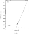
- These structures thus represent, in principle, p-n heterojunctions, although the layers are too thin to allow accurate measurements. Nevertheless, the rectifying character of this structure is evident from the I-V measurements such as displayed in Fig. 2 (a).
- the linear behavior of the forward I-V curve is caused by the contact resistance of the junction, which was thus estimated to be about 4k ⁇ .
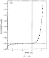
- the forward current depends exponentially on voltage as shown in Fig. 2 (b).
- the turn-on voltage is about 1.5 V, and the breakdown of the p-n junction of 5 V of reverse bias corresponds to an electric field of 10 6 V/cm, which is more than twice as high than that found for other III-V semiconductors such as GaAs and InP.
- the present invention can be used with any semiconductor components or devices which have one or more layers of p-type conductivity, such as light-emitting diodes, rectifying diodes, laser diodes or bipolar transistors. It is not necessary to describe the layer structures of these components here since the basic layer structures are well known per se and the present invention lies in realising the p-type layer or layers using the codoping technique described herein.
Landscapes
- Led Devices (AREA)
- Liquid Deposition Of Substances Of Which Semiconductor Devices Are Composed (AREA)
Priority Applications (1)
| Application Number | Priority Date | Filing Date | Title |
|---|---|---|---|
| EP97107630A EP0807978A3 (fr) | 1996-05-10 | 1997-05-09 | Méthode pour fabriquer une couche de forte conductivité de type P dans un composant semi-conducteur et composant semi-conducteur comprenant une telle couche |
Applications Claiming Priority (3)
| Application Number | Priority Date | Filing Date | Title |
|---|---|---|---|
| EP96107454 | 1996-05-10 | ||
| EP96107454 | 1996-05-10 | ||
| EP97107630A EP0807978A3 (fr) | 1996-05-10 | 1997-05-09 | Méthode pour fabriquer une couche de forte conductivité de type P dans un composant semi-conducteur et composant semi-conducteur comprenant une telle couche |
Publications (2)
| Publication Number | Publication Date |
|---|---|
| EP0807978A2 true EP0807978A2 (fr) | 1997-11-19 |
| EP0807978A3 EP0807978A3 (fr) | 1997-11-26 |
Family
ID=26141924
Family Applications (1)
| Application Number | Title | Priority Date | Filing Date |
|---|---|---|---|
| EP97107630A Withdrawn EP0807978A3 (fr) | 1996-05-10 | 1997-05-09 | Méthode pour fabriquer une couche de forte conductivité de type P dans un composant semi-conducteur et composant semi-conducteur comprenant une telle couche |
Country Status (1)
| Country | Link |
|---|---|
| EP (1) | EP0807978A3 (fr) |
Cited By (2)
| Publication number | Priority date | Publication date | Assignee | Title |
|---|---|---|---|---|
| EP0902487A3 (fr) * | 1997-09-05 | 2000-10-25 | Honnavalli R. Vydyanath | Dispositif semi-conducteur et sa méthode de fabrication |
| GB2344462B (en) * | 1998-12-02 | 2001-05-16 | Arima Optoelectronics Corp | Semiconductor devices |
Family Cites Families (2)
| Publication number | Priority date | Publication date | Assignee | Title |
|---|---|---|---|---|
| US3649384A (en) * | 1969-03-27 | 1972-03-14 | Norton Research Corp | Process for fabricating silicon carbide junction diodes by liquid phase epitaxial growth |
| US5150191A (en) * | 1989-11-21 | 1992-09-22 | Kabushiki Kaisha Toshiba | P-type II-VI compound semiconductor doped |
-
1997
- 1997-05-09 EP EP97107630A patent/EP0807978A3/fr not_active Withdrawn
Cited By (2)
| Publication number | Priority date | Publication date | Assignee | Title |
|---|---|---|---|---|
| EP0902487A3 (fr) * | 1997-09-05 | 2000-10-25 | Honnavalli R. Vydyanath | Dispositif semi-conducteur et sa méthode de fabrication |
| GB2344462B (en) * | 1998-12-02 | 2001-05-16 | Arima Optoelectronics Corp | Semiconductor devices |
Also Published As
| Publication number | Publication date |
|---|---|
| EP0807978A3 (fr) | 1997-11-26 |
Similar Documents
| Publication | Publication Date | Title |
|---|---|---|
| US5818072A (en) | Integrated heterostructure of group II-VI semiconductor materials including epitaxial ohmic contact and method of fabricating same | |
| US7622398B2 (en) | Semiconductor device, semiconductor layer and production method thereof | |
| Sheu et al. | Photoluminescence spectroscopy of Mg-doped GaN | |
| Johnson et al. | Molecular beam epitaxy growth and properties of GaN, Al x Ga1− x N, and AlN on GaN/SiC substrates | |
| Suemune et al. | Epitaxial ZnO growth and p‐type doping with MOMBE | |
| US6831304B2 (en) | P-n junction type boron phosphide-based semiconductor light-emitting device and production method thereof | |
| Allenic et al. | Microstructure and electrical properties of p-type phosphorus-doped ZnO films | |
| Ren et al. | Integrated heterostructure devices composed of II–VI materials with Hg-based contact layers | |
| Lo | Cd‐diffused Pb1− xSnxTe lasers with high output power | |
| Nikolaev et al. | GaN pn-structures grown by hydride vapor phase epitaxy | |
| Fan et al. | Electrical properties of blue/green diode lasers | |
| Jeon et al. | Molecular beam epitaxial growth of green light emitting diodes on ZnSe wafers | |
| Pann et al. | Effect of indium on the properties of DX centers in Si‐doped In y (Ga0. 3Al0. 7) 1− y As | |
| Enstrom et al. | Influence of Gas‐Phase Stoichiometry on the Defect Morphology, Impurity Doping, and Electroluminescence Efficiency of Vapor‐Grown GaAs P‐N Junctions | |
| Nuese et al. | Vapor-grown In1− xGaxP electroluminescent junctions on GaAs | |
| Kato et al. | Postgrowth of a Si contact layer on an air‐exposed Si1− x Ge x/Si single quantum well grown by gas‐source molecular beam epitaxy, for use in an electroluminescent device | |
| Tsang et al. | All‐gaseous doping during chemical‐beam epitaxial growth of InGaAs/InGaAsP multi‐quantum‐well lasers | |
| Deppe et al. | Buried heterostructure Al x Ga1− x As‐GaAs quantum well lasers by Ge diffusion from the vapor | |
| EP0902487A2 (fr) | Dispositif semi-conducteur et sa méthode de fabrication | |
| Chellic et al. | Minority carrier lifetime in MOCVD-grown C-and Zn-doped InGaAs | |
| Gunshor et al. | The molecular beam epitaxial growth of wide gap II–VI injection lasers and light-emitting diodes | |
| Kim et al. | Co-doping characteristics of Si and Zn with Mg in p-type GaN | |
| Voronina et al. | Influence of tellurium impurity on the Properties of Ga1− X InXAsYSb1− Y (X> 0.22) solid solutions | |
| Lian et al. | High-quality carbon-doped GaAs/AlGaAs material growth in MOCVD and its application for optoelectronic devices | |
| WO2003054976A1 (fr) | Dispositif semiconducteur a base de phosphure de bore et procede de production dudit dispositif |
Legal Events
| Date | Code | Title | Description |
|---|---|---|---|
| PUAI | Public reference made under article 153(3) epc to a published international application that has entered the european phase |
Free format text: ORIGINAL CODE: 0009012 |
|
| PUAL | Search report despatched |
Free format text: ORIGINAL CODE: 0009013 |
|
| AK | Designated contracting states |
Kind code of ref document: A2 Designated state(s): DE FR GB NL |
|
| AK | Designated contracting states |
Kind code of ref document: A3 Designated state(s): AT BE CH DE DK ES FI FR GB GR IE IT LI LU MC NL PT SE |
|
| RBV | Designated contracting states (corrected) |
Designated state(s): DE FR GB NL |
|
| 17P | Request for examination filed |
Effective date: 19980526 |
|
| STAA | Information on the status of an ep patent application or granted ep patent |
Free format text: STATUS: THE APPLICATION IS DEEMED TO BE WITHDRAWN |
|
| 18D | Application deemed to be withdrawn |
Effective date: 20011203 |