EP0807835A2 - Monolithcally integrated optical semiconductor component - Google Patents
Monolithcally integrated optical semiconductor component Download PDFInfo
- Publication number
- EP0807835A2 EP0807835A2 EP97401048A EP97401048A EP0807835A2 EP 0807835 A2 EP0807835 A2 EP 0807835A2 EP 97401048 A EP97401048 A EP 97401048A EP 97401048 A EP97401048 A EP 97401048A EP 0807835 A2 EP0807835 A2 EP 0807835A2
- Authority
- EP
- European Patent Office
- Prior art keywords
- waveguide
- layer
- brs
- passive
- active
- Prior art date
- Legal status (The legal status is an assumption and is not a legal conclusion. Google has not performed a legal analysis and makes no representation as to the accuracy of the status listed.)
- Withdrawn
Links
Images


Classifications
-
- G—PHYSICS
- G02—OPTICS
- G02B—OPTICAL ELEMENTS, SYSTEMS OR APPARATUS
- G02B6/00—Light guides; Structural details of arrangements comprising light guides and other optical elements, e.g. couplings
- G02B6/10—Light guides; Structural details of arrangements comprising light guides and other optical elements, e.g. couplings of the optical waveguide type
- G02B6/12—Light guides; Structural details of arrangements comprising light guides and other optical elements, e.g. couplings of the optical waveguide type of the integrated circuit kind
- G02B6/12004—Combinations of two or more optical elements
-
- B—PERFORMING OPERATIONS; TRANSPORTING
- B82—NANOTECHNOLOGY
- B82Y—SPECIFIC USES OR APPLICATIONS OF NANOSTRUCTURES; MEASUREMENT OR ANALYSIS OF NANOSTRUCTURES; MANUFACTURE OR TREATMENT OF NANOSTRUCTURES
- B82Y20/00—Nanooptics, e.g. quantum optics or photonic crystals
-
- G—PHYSICS
- G02—OPTICS
- G02B—OPTICAL ELEMENTS, SYSTEMS OR APPARATUS
- G02B6/00—Light guides; Structural details of arrangements comprising light guides and other optical elements, e.g. couplings
- G02B6/10—Light guides; Structural details of arrangements comprising light guides and other optical elements, e.g. couplings of the optical waveguide type
- G02B6/12—Light guides; Structural details of arrangements comprising light guides and other optical elements, e.g. couplings of the optical waveguide type of the integrated circuit kind
- G02B6/122—Basic optical elements, e.g. light-guiding paths
- G02B6/125—Bends, branchings or intersections
-
- H—ELECTRICITY
- H01—ELECTRIC ELEMENTS
- H01S—DEVICES USING THE PROCESS OF LIGHT AMPLIFICATION BY STIMULATED EMISSION OF RADIATION [LASER] TO AMPLIFY OR GENERATE LIGHT; DEVICES USING STIMULATED EMISSION OF ELECTROMAGNETIC RADIATION IN WAVE RANGES OTHER THAN OPTICAL
- H01S5/00—Semiconductor lasers
- H01S5/02—Structural details or components not essential to laser action
- H01S5/026—Monolithically integrated components, e.g. waveguides, monitoring photo-detectors, drivers
-
- G—PHYSICS
- G02—OPTICS
- G02B—OPTICAL ELEMENTS, SYSTEMS OR APPARATUS
- G02B6/00—Light guides; Structural details of arrangements comprising light guides and other optical elements, e.g. couplings
- G02B6/10—Light guides; Structural details of arrangements comprising light guides and other optical elements, e.g. couplings of the optical waveguide type
- G02B6/12—Light guides; Structural details of arrangements comprising light guides and other optical elements, e.g. couplings of the optical waveguide type of the integrated circuit kind
- G02B2006/12083—Constructional arrangements
- G02B2006/121—Channel; buried or the like
-
- G—PHYSICS
- G02—OPTICS
- G02B—OPTICAL ELEMENTS, SYSTEMS OR APPARATUS
- G02B6/00—Light guides; Structural details of arrangements comprising light guides and other optical elements, e.g. couplings
- G02B6/10—Light guides; Structural details of arrangements comprising light guides and other optical elements, e.g. couplings of the optical waveguide type
- G02B6/12—Light guides; Structural details of arrangements comprising light guides and other optical elements, e.g. couplings of the optical waveguide type of the integrated circuit kind
- G02B2006/12166—Manufacturing methods
- G02B2006/12169—Annealing
-
- G—PHYSICS
- G02—OPTICS
- G02B—OPTICAL ELEMENTS, SYSTEMS OR APPARATUS
- G02B6/00—Light guides; Structural details of arrangements comprising light guides and other optical elements, e.g. couplings
- G02B6/10—Light guides; Structural details of arrangements comprising light guides and other optical elements, e.g. couplings of the optical waveguide type
- G02B6/12—Light guides; Structural details of arrangements comprising light guides and other optical elements, e.g. couplings of the optical waveguide type of the integrated circuit kind
- G02B2006/12166—Manufacturing methods
- G02B2006/12173—Masking
-
- G—PHYSICS
- G02—OPTICS
- G02B—OPTICAL ELEMENTS, SYSTEMS OR APPARATUS
- G02B6/00—Light guides; Structural details of arrangements comprising light guides and other optical elements, e.g. couplings
- G02B6/10—Light guides; Structural details of arrangements comprising light guides and other optical elements, e.g. couplings of the optical waveguide type
- G02B6/12—Light guides; Structural details of arrangements comprising light guides and other optical elements, e.g. couplings of the optical waveguide type of the integrated circuit kind
- G02B2006/12166—Manufacturing methods
- G02B2006/12176—Etching
-
- H—ELECTRICITY
- H01—ELECTRIC ELEMENTS
- H01S—DEVICES USING THE PROCESS OF LIGHT AMPLIFICATION BY STIMULATED EMISSION OF RADIATION [LASER] TO AMPLIFY OR GENERATE LIGHT; DEVICES USING STIMULATED EMISSION OF ELECTROMAGNETIC RADIATION IN WAVE RANGES OTHER THAN OPTICAL
- H01S5/00—Semiconductor lasers
- H01S5/20—Structure or shape of the semiconductor body to guide the optical wave ; Confining structures perpendicular to the optical axis, e.g. index or gain guiding, stripe geometry, broad area lasers, gain tailoring, transverse or lateral reflectors, special cladding structures, MQW barrier reflection layers
- H01S5/2054—Methods of obtaining the confinement
- H01S5/2059—Methods of obtaining the confinement by means of particular conductivity zones, e.g. obtained by particle bombardment or diffusion
- H01S5/2063—Methods of obtaining the confinement by means of particular conductivity zones, e.g. obtained by particle bombardment or diffusion obtained by particle bombardment
-
- H—ELECTRICITY
- H01—ELECTRIC ELEMENTS
- H01S—DEVICES USING THE PROCESS OF LIGHT AMPLIFICATION BY STIMULATED EMISSION OF RADIATION [LASER] TO AMPLIFY OR GENERATE LIGHT; DEVICES USING STIMULATED EMISSION OF ELECTROMAGNETIC RADIATION IN WAVE RANGES OTHER THAN OPTICAL
- H01S5/00—Semiconductor lasers
- H01S5/30—Structure or shape of the active region; Materials used for the active region
- H01S5/32—Structure or shape of the active region; Materials used for the active region comprising PN junctions, e.g. hetero- or double- heterostructures
- H01S5/3206—Structure or shape of the active region; Materials used for the active region comprising PN junctions, e.g. hetero- or double- heterostructures ordering or disordering the natural superlattice in ternary or quaternary materials
-
- H—ELECTRICITY
- H01—ELECTRIC ELEMENTS
- H01S—DEVICES USING THE PROCESS OF LIGHT AMPLIFICATION BY STIMULATED EMISSION OF RADIATION [LASER] TO AMPLIFY OR GENERATE LIGHT; DEVICES USING STIMULATED EMISSION OF ELECTROMAGNETIC RADIATION IN WAVE RANGES OTHER THAN OPTICAL
- H01S5/00—Semiconductor lasers
- H01S5/30—Structure or shape of the active region; Materials used for the active region
- H01S5/32—Structure or shape of the active region; Materials used for the active region comprising PN junctions, e.g. hetero- or double- heterostructures
- H01S5/3211—Structure or shape of the active region; Materials used for the active region comprising PN junctions, e.g. hetero- or double- heterostructures characterised by special cladding layers, e.g. details on band-discontinuities
-
- H—ELECTRICITY
- H01—ELECTRIC ELEMENTS
- H01S—DEVICES USING THE PROCESS OF LIGHT AMPLIFICATION BY STIMULATED EMISSION OF RADIATION [LASER] TO AMPLIFY OR GENERATE LIGHT; DEVICES USING STIMULATED EMISSION OF ELECTROMAGNETIC RADIATION IN WAVE RANGES OTHER THAN OPTICAL
- H01S5/00—Semiconductor lasers
- H01S5/30—Structure or shape of the active region; Materials used for the active region
- H01S5/34—Structure or shape of the active region; Materials used for the active region comprising quantum well or superlattice structures, e.g. single quantum well [SQW] lasers, multiple quantum well [MQW] lasers or graded index separate confinement heterostructure [GRINSCH] lasers
- H01S5/343—Structure or shape of the active region; Materials used for the active region comprising quantum well or superlattice structures, e.g. single quantum well [SQW] lasers, multiple quantum well [MQW] lasers or graded index separate confinement heterostructure [GRINSCH] lasers in AIIIBV compounds, e.g. AlGaAs-laser, InP-based laser
- H01S5/34306—Structure or shape of the active region; Materials used for the active region comprising quantum well or superlattice structures, e.g. single quantum well [SQW] lasers, multiple quantum well [MQW] lasers or graded index separate confinement heterostructure [GRINSCH] lasers in AIIIBV compounds, e.g. AlGaAs-laser, InP-based laser emitting light at a wavelength longer than 1000nm, e.g. InP based 1300 and 1500nm lasers
-
- H—ELECTRICITY
- H01—ELECTRIC ELEMENTS
- H01S—DEVICES USING THE PROCESS OF LIGHT AMPLIFICATION BY STIMULATED EMISSION OF RADIATION [LASER] TO AMPLIFY OR GENERATE LIGHT; DEVICES USING STIMULATED EMISSION OF ELECTROMAGNETIC RADIATION IN WAVE RANGES OTHER THAN OPTICAL
- H01S5/00—Semiconductor lasers
- H01S5/30—Structure or shape of the active region; Materials used for the active region
- H01S5/34—Structure or shape of the active region; Materials used for the active region comprising quantum well or superlattice structures, e.g. single quantum well [SQW] lasers, multiple quantum well [MQW] lasers or graded index separate confinement heterostructure [GRINSCH] lasers
- H01S5/343—Structure or shape of the active region; Materials used for the active region comprising quantum well or superlattice structures, e.g. single quantum well [SQW] lasers, multiple quantum well [MQW] lasers or graded index separate confinement heterostructure [GRINSCH] lasers in AIIIBV compounds, e.g. AlGaAs-laser, InP-based laser
- H01S5/34313—Structure or shape of the active region; Materials used for the active region comprising quantum well or superlattice structures, e.g. single quantum well [SQW] lasers, multiple quantum well [MQW] lasers or graded index separate confinement heterostructure [GRINSCH] lasers in AIIIBV compounds, e.g. AlGaAs-laser, InP-based laser with a well layer having only As as V-compound, e.g. AlGaAs, InGaAs
-
- H—ELECTRICITY
- H01—ELECTRIC ELEMENTS
- H01S—DEVICES USING THE PROCESS OF LIGHT AMPLIFICATION BY STIMULATED EMISSION OF RADIATION [LASER] TO AMPLIFY OR GENERATE LIGHT; DEVICES USING STIMULATED EMISSION OF ELECTROMAGNETIC RADIATION IN WAVE RANGES OTHER THAN OPTICAL
- H01S5/00—Semiconductor lasers
- H01S5/30—Structure or shape of the active region; Materials used for the active region
- H01S5/34—Structure or shape of the active region; Materials used for the active region comprising quantum well or superlattice structures, e.g. single quantum well [SQW] lasers, multiple quantum well [MQW] lasers or graded index separate confinement heterostructure [GRINSCH] lasers
- H01S5/343—Structure or shape of the active region; Materials used for the active region comprising quantum well or superlattice structures, e.g. single quantum well [SQW] lasers, multiple quantum well [MQW] lasers or graded index separate confinement heterostructure [GRINSCH] lasers in AIIIBV compounds, e.g. AlGaAs-laser, InP-based laser
- H01S5/3434—Structure or shape of the active region; Materials used for the active region comprising quantum well or superlattice structures, e.g. single quantum well [SQW] lasers, multiple quantum well [MQW] lasers or graded index separate confinement heterostructure [GRINSCH] lasers in AIIIBV compounds, e.g. AlGaAs-laser, InP-based laser with a well layer comprising at least both As and P as V-compounds
Definitions
- the invention relates to a monolithically integrated optical semiconductor component according to the preamble of claim 1 and a manufacturing method according to the preamble of claim 8.
- Such a semiconductor component is used for signal generation, signal regeneration, signal processing or for switching signals in optical communication, in particular in optical transmission networks which work largely without optoelectronic signal conversion.
- active waveguide regions such as e.g. Lasers, switches, modulators, amplifiers or detectors with passive waveguide areas such as passive waveguides, splitters, filters or couplers integrated monolithically.
- a buried strip waveguide laser that is monolithically integrated with a passive waveguide is known from an article by D. Remiens et al (Buried Ridge Stripe Lasers Monolithically Integrated with Butt-Coupled Passive Waveguides for OEIC, SPIE Vol. 1362, p. 323 -330).
- the passive waveguide is also a buried strip waveguide, which has a p-doped cover layer is covered.
- high absorption losses in the passive waveguide are disadvantageous.
- the laser is manufactured by a process that contains several steps that require precise adjustment of the laser on lithography masks.
- buried strip waveguides are preferably used in the active waveguide regions in monolithically integrated semiconductor components for many applications.
- U. Koren et al Semi-Insulating Blocked Planar BH GaInAsP / InP Laser with High Power and High Modulation Bandwidth, Elektr. Lett. Vol. 24 No. 3 1988, known, this waveguide structure is particularly suitable for lasers due to the low threshold current, the high achievable output power and the long service life, but it is also used for integrated amplifiers and switches.
- T. Koch et al Semiconductor Photonic Integrated Circuits, IEEE J. Quant. Vol. 27 No.
- the component according to the invention also has the advantage that the passive waveguide regions are insulated by the cladding layer, since the transition from p-doped to n-doped semiconductor layers is interrupted and therefore no parasitic currents can flow through the passive waveguide regions. This leads to improved high-frequency properties of the semiconductor component, i.e. to an expanded frequency response.
- FIG. 1 shows a section through a first exemplary embodiment of an optical semiconductor component BE1 according to the invention.
- the section runs along a strip waveguide BRS buried in the optical semiconductor component BE1.
- the optical semiconductor component BE1 has a substrate SUB, on which the strip waveguide BRS rests.
- This strip waveguide BRS has an active, i.e. controlled light-amplifying or light-absorbing waveguide region AB and a passive, i.e. Light-transmitting waveguide area PB without amplification.
- the strip waveguide is covered by a cladding layer MS in the passive waveguide region PB.
- the semiconductor component BE1 is covered over the entire area by a cover layer DS and a contact layer KS.
- a cover layer DS In the active waveguide area AB there is also a metal contact MK2 above the strip waveguide BRS on the contact layer KS.
- the underside of the substrate SUB is coated over the entire area with a metal contact layer MK1.
- the buried strip waveguide BRS contains at least one optically active layer MQW.
- This at least one optically active layer MQW is preferably a multi-quantum well structure, i.e. a layer stack containing semiconductor layers with alternating small and large band gap energy.
- Bandgap energy is the energetic distance between the valence and conduction bands of a semiconductor.
- charge carriers electrospray carriers
- the transition energy of which is referred to below as the energy band gap.
- the thickness of these semiconductor layers determines the size of the energy band gap and thus the wavelength at which light is absorbed, amplified or emitted in the strip waveguide BRS.
- the wavelength at which light is amplified or absorbed in a controlled manner in the active waveguide region is referred to as the working wavelength ⁇ .
- the working wavelength is determined by the material composition of this layer.
- the semiconductor component BE1 is designed by suitable selection of the layer thicknesses of the semiconductor layers with the small and with the large bandgap energy for light signals with a working wavelength ⁇ of 1550 nm.
- the working wavelength ⁇ is usually in a range from 1530 nm to 1580 nm for message transmission over long distances.
- the energy band gap is larger or smaller than in the active waveguide area AB.
- light of the working wavelength ⁇ is hardly or at least less strongly absorbed in the passive waveguide region PB than would be the case with the same energy band gap.
- the at least one optically active layer MQW is hatched differently in the active waveguide region AB in FIG. 1 than in the passive PB.
- the strip waveguide BRS contains waveguide layers SCH which enclose the at least one optically active layer MQW in the direction perpendicular to the substrate plane.
- These waveguide layers SCH have a refractive index that is greater than the refractive index of the surrounding semiconductor material of the top layer DS, cladding layer MS and substrate SUB. As a result, a light wave is guided in the buried strip waveguide BRS.
- the cover layer DS has an absorption coefficient for light signals of the working wavelength ⁇ . This absorption coefficient indicates how strongly a light wave in the material is attenuated by absorption over a certain distance.
- the cladding layer MS has an absorption coefficient that is smaller than the absorption coefficient of the top layer DS. I.e. a light wave in the material of the cladding layer MS is weakened less strongly by absorption over the same distance than in the material of the top layer DS.
- the strip waveguide BRS If a light wave is guided in the strip waveguide BRS, certain portions of this light wave also propagate in the material that surrounds the strip waveguide, ie in the material of the substrate SUB, the cover layer DS or the cladding layer MS.
- the strip waveguide BRS In the passive waveguide region PB, the strip waveguide BRS is covered by the cladding layer, which has a smaller absorption coefficient than the cover layer DS, which covers the strip waveguide in the active waveguide region AB. As a result, absorption losses in the passive waveguide region are reduced.
- the cladding layer MS As explained, it is the task of the cladding layer MS to reduce absorption losses in the passive waveguide region PB. These absorption losses result primarily from interval band transitions in p-doped semiconductor material, from which the cover layer DS consists in the exemplary embodiment.
- the cladding layer MS consists of undoped or semi-insulating semiconductor material. Semi-insulating semiconductor material is characterized in that it has recombination sites for radiationless transitions, so that free charge carriers (electrons and holes) recombine at these recombination sites before they can interact with a light wave.
- An example of such a semi-insulating semiconductor material is Fe- or Cr-doped InP.
- a cladding layer MS made of such semiconductor material is applied only in the passive waveguide region PB above the strip waveguide BRS.
- the strip waveguide BRS is directly covered by the cover layer DS, which has a doping of the opposite conductivity type as the substrate SUB.
- the substrate is n-doped.
- the refractive index of the cladding layer MS is the same size as the refractive index of the cover layer DS. Then there is no change in the refractive index in the semiconductor material which surrounds the buried strip waveguide BRS between the active waveguide region AB and the passive waveguide region PB. As a result, the properties of the optical waveguide of the buried strip waveguide BRS in the active AB and passive PB waveguide region are the same and there are no scatter losses and reflections.
- the strip waveguide BRS consists both in the active AB and in the passive PB waveguide region of a continuous, coherent semiconductor layer package, which is applied in a single coating process.
- the strip waveguide BRS has a semiconductor layer package with a multi-quantum well structure MQW and consists of a continuous, coherent semiconductor layer package, the semiconductor layers of the multi-quantum well layers MQW having a greater layer thickness in the active waveguide region AB than in the passive PB.
- the layer thickness of these semiconductor layers determines the energy band gap of the multi-quantum well structure and thus the wavelength at which light is absorbed, emitted or amplified.
- FIGS. 2a and 2b show the same optical semiconductor component BE1 as in FIG. 1.
- FIG. 2a shows a section perpendicular to the strip waveguide BRS in the active waveguide region AB
- FIG. 2b shows a section perpendicular to the strip waveguide BRS in the passive waveguide region PB.
- the mesa-shaped strip waveguide BRS can be seen, which lies on the substrate SUB and is completely covered by the cover layer DS.
- the areas NL of the cover layer DS on both sides of the strip waveguide BRS are made non-conductive, for example by ion implantation, preferably implantation of protons, so that an operating current is restricted to the area of the strip waveguide BRS.
- On the cover layer DS there is a highly doped contact layer KS and a metal contact MK2, which is applied to the contact layer KS above the strip waveguide BRS.
- the cladding layer MS is additionally located between the cover layer DS and the strip waveguide BRS. Non-conductive areas in the cover layer DS and a metal contact on the contact layer KS are not provided in the passive waveguide area PB.
- the substrate SUB consists of n-doped InP
- the cover layer DS consists of p-doped InP
- the contact layer consists of p + -doped (highly doped) InGaAsP
- the waveguide and multi-quantum well layers consist of ternary or quaternary mixed crystals of III / V connection type such as InGaAsP, InGaAs, InGaAlAs or similar.
- the cladding layer MS is made of undoped or semi-insulating InP.
- III / V connection type such as GaAs
- Possible materials are also semiconductors of the II / VI or IV / IV connection type.
- FIGS. 3 to 7 schematically show a second exemplary embodiment of a semiconductor component BE2 according to the invention after various steps of a manufacturing method according to the invention.
- FIG. 3 shows a substrate SUB, to which a mesa-striped strip waveguide BRS was applied in a first step.
- the strip waveguide BRS forms a Y-shaped branch.
- a semiconductor layer package is applied over the entire surface of the substrate SUB in a first sub-step.
- this semiconductor layer package consists of a first waveguide layer SCH1, an optically active layer package with a multi-quantum well structure MQW and a second waveguide layer SCH2.
- the semiconductor layer package can be applied by epitaxial deposition of semiconductor material from the liquid phase (LPE) or from the gas phase (MOVPE).
- the semiconductor layer package by means of molecular beam epitaxy using the gas source molecular beam epitaxy method (GSMBE), since in this method the layer thicknesses and thus the energy band gap of the multi-quantum well structure are spread over a large coating area. such as have the area of a wafer with a diameter of 2 inches checked well.
- GMBE gas source molecular beam epitaxy method
- active and passive waveguide regions are formed from the semiconductor layer package, specifically in such a way that the energy band gap in the active waveguide regions is different from that in the passive ones.
- the parts of the semiconductor layer package provided as passive waveguide regions are bombarded with ions, as a result of which lattice defects are generated.
- the semiconductor component BE2 is then heated and annealed, as a result of which the lattice defects largely heal again.
- This treatment shifts the energy band gap of the multi-quantum well structure to shorter wavelengths.
- the strip waveguide BRS thus formed is a continuous, coherent part of the semiconductor layer package. As a result, there are no joints in the finished semiconductor component BE2 between active and passive waveguide regions at which different semiconductor layers in the strip waveguide are put together in the direction of light propagation. This prevents reflections and wastage.
- Another method is the process known as butt coupling.
- the parts of the semiconductor layer package provided as passive waveguide regions are removed and replaced by selective growth with a new layer package with a different energy band gap.
- an etching mask is produced on the semiconductor layer package by means of photolithography.
- the etching mask consists of photoresist and covers the areas of the semiconductor layer package from which the strip waveguide BRS is formed.
- the semiconductor layer package is etched, so that a mesa-shaped strip remains as a strip waveguide BRS on the substrate SUB. This can be done, for example, by wet chemical etching with an etchant. The areas of the semiconductor layer package covered by the etching mask are not detached by the etching agent.
- the etching mask is then removed with a solvent.
- a dielectric mask is applied to the substrate SUB, for example made of SiO 2 .
- This dielectric mask is structured by means of photolithography and etching, for example with buffered hydrofluoric acid, in such a way that narrow strips in which the strip waveguide is to be formed remain free.
- the narrow strip is laterally delimited by areas which are masked over a large area.
- passive waveguide areas there is no lateral limitation by the dielectric mask or there is only a narrow dielectric, lateral masking.
- a semiconductor layer package is applied which contains a first waveguide layer SCH1, a layer package with a multi-quantum well structure MQW and a second waveguide layer SCH2.
- the metal-organic vapor-phase epitaxy (MOVPE) process is used for this, in which semiconductor material is deposited from the gas phase. This is preferably done at a pressure of 100-150 mbar. No semiconductor material is deposited on the dielectric mask. Migration and diffusion in the gas phase directly above the dielectric mask increase the growth rate on neighboring, unmasked areas of the substrate surface.
- MOVPE metal-organic vapor-phase epitaxy
- Semiconductor layers in the active regions which are laterally delimited by a dielectric mask over a large area, therefore grow thicker than semiconductor layers in passive regions which are not delimited or only laterally by a narrow dielectric mask.
- the dielectric mask is removed again, for example with buffered hydrofluoric acid.
- the semiconductor layer package formed in this way consists of semiconductor layers which have a greater layer thickness in the active waveguide regions than in the passive waveguide regions.
- the energy band gap of the multi-quantum well structure MQW is 1550 nm in the active waveguide regions and 1430 nm in the passive waveguide regions.
- the strip waveguide BRS can now be formed from the semiconductor layer package by etching using an etching mask made of photoresist.
- a dielectric layer MASK is applied to the semiconductor component BE2 and structured photolithographically in such a way that it covers the parts of the strip waveguide provided as active regions, including the parts of the substrate surface adjoining them. As shown in FIG. 4, the covered area can be many times larger than the width of the strip waveguide BRS.
- the dielectric layer MASK can be made of SiO 2 or SiN, for example. 4 shows the semiconductor component BE2 after this second step.
- a cladding layer MS is applied.
- This cladding layer is made of undoped or semi-insulating semiconductor material.
- Epitaxial deposition from the gas phase using the MOVPE method is particularly suitable, but liquid phases (LPE) or molecular beam epitaxy (GSMBE) are also suitable for depositing the cladding layer MS.
- LPE liquid phases
- GMBE molecular beam epitaxy
- No or only policrystalline semiconductor material is deposited on the dielectric layer MASK, so that only the passive waveguide regions are covered by the cladding layer MS.
- the semiconductor component BE2 after this third step is shown in FIG. 5.
- the dielectric layer MASK is then removed again. If the dielectric layer MASK consists, for example, of SiO 2 , buffered hydrofluoric acid can be used for this, which selectively removes SiO 2 . This step exposes the BRS strip waveguide in the active areas.
- FIG. 6 shows the semiconductor component BE2 after this fourth step.
- a cover layer DS and a contact layer KS are now applied over the entire surface.
- This can e.g. by epitaxial deposition of semiconductor material from the liquid phase (LPE) or from the gas phase (MOVPE) or by means of molecular beam epitaxy (GSMBE).
- Cover layer DS and contact layer KS have a doping of the opposite conductivity type as the substrate SUB.
- the strip waveguide BRS is completely covered by the cover layer DS both in the active waveguide regions AB1-AB3 and in the passive waveguide regions PB, and in the passive waveguide regions PB there is also the cladding layer MS between the strip waveguide BRS and the cover layer DS.
- FIG. 7 shows the semiconductor component BE2 after this fifth step.
- the regions of the cover layer DS on both sides of the strip waveguide BRS can be made non-conductive by implantation of ions, preferably protons.
- ions preferably protons.
- a metal contact is applied to the contact layer KS in the active waveguide regions AB1-AB3 above the strip waveguide BRS.
- the semiconductor component BE2 in the second exemplary embodiment contains a first active waveguide region AB1, which is divided into a passive waveguide region PB with a y-shaped branching into two partial waveguides.
- the two partial waveguides each have a further active waveguide area AB2, AB3.
- Such an arrangement serves e.g. as an element for a cascaded optical space switch, as specified in EP 616 243 A.
- a light signal which is radiated into the first active waveguide region AB1 can optionally be passed on to one or both partial waveguides.
- the first active waveguide area AB1 serves as an input amplifier and the two further active waveguide areas AB2, AB3 serve as switches and can be controlled either translucent or opaque.
- a cascaded optical space switch can be formed by interconnecting a large number of such semiconductor components BE2 on a common substrate.
Landscapes
- Physics & Mathematics (AREA)
- Engineering & Computer Science (AREA)
- Optics & Photonics (AREA)
- General Physics & Mathematics (AREA)
- Microelectronics & Electronic Packaging (AREA)
- Nanotechnology (AREA)
- Chemical & Material Sciences (AREA)
- Biophysics (AREA)
- Life Sciences & Earth Sciences (AREA)
- Electromagnetism (AREA)
- Crystallography & Structural Chemistry (AREA)
- Condensed Matter Physics & Semiconductors (AREA)
- Optical Integrated Circuits (AREA)
- Semiconductor Lasers (AREA)
- Optical Modulation, Optical Deflection, Nonlinear Optics, Optical Demodulation, Optical Logic Elements (AREA)
- Light Receiving Elements (AREA)
Abstract
Monolithisch integrierte optische Halbleiterbauelemente mit vergrabenem Streifenwellenleiter (BRS) werden in der optischen Nachrichtenübertragung eingesetzt. Sie enthalten aktive (AB) und passive (PB) Wellenleiterbereiche. Bei passiven Wellenleiterbereichen mit vergrabenem Streifenwellenleiter treten hohe Absorbtionsverluste auf, wogegen es bei passiven Wellenleiterbereichen mit verlustarmen Rippenwellenleitern zu Reflexionen und Streuverlusten an der Stoßstelle zu aktiven Wellenleiterbereichen kommt.Monolithically integrated optical semiconductor components with buried strip waveguide (BRS) are used in optical communication. They contain active (AB) and passive (PB) waveguide areas. In the case of passive waveguide regions with buried strip waveguides, high absorption losses occur, whereas in the case of passive waveguide regions with low-loss rib waveguides, reflections and scatter losses occur at the joint to active waveguide regions.
Ein erfindungsgemäßes Halbleiterbauelement (BE2) besitzt in aktiven (AB) wie in passiven (PB) Wellenleiterbereichen einen vergrabenen Streifenwellenleiter (BRS), der von einer Deckschicht (DS) bedeckt ist. Zusätzlich befindet sich in den passiven Bereichen (PB) zwischen Streifenwellenleiter (BRS) und Deckschicht (DS) eine semiisolierende oder undotierte Mantelschicht (MS).A semiconductor component (BE2) according to the invention has a buried strip waveguide (BRS) in active (AB) and in passive (PB) waveguide regions, which is covered by a cover layer (DS). In addition, a semi-insulating or undoped cladding layer (MS) is located in the passive areas (PB) between the strip waveguide (BRS) and the top layer (DS).
Desweiteren ist auch ein Verfahren angegeben, nach dem ein erfindungsgemäßes Halbleiterbauelement hergestellt werden kann.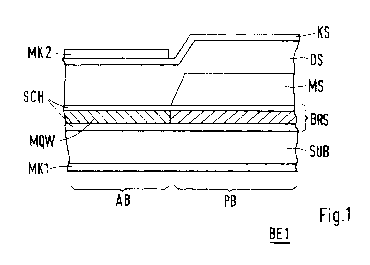
Description
Die Erfindung betrifft ein monolithisch integriertes optisches Halbleiterbauelement gemäß dem Oberbegriff des Anspruchs 1 und ein Herstellungsverfahren gemäß dem Oberbegriff des Anspruchs 8.The invention relates to a monolithically integrated optical semiconductor component according to the preamble of
Ein solches Halbleiterbauelement wird zur Signalerzeugung, Signalregeneration, Signalverarbeitung oder zum Schalten von Signalen in der optischen Nachrichtenübertragung eingesetzt, insbesondere in optischen Übertragungsnetzen, die weitgehend ohne optoelektronische Signalwandlung arbeiten. Dazu sind in dem Halbleiterbauelement aktive Wellenleiterbereiche wie z.B. Laser, Schalter, Modulatoren, Verstärker oder Detektoren mit passiven Wellenleiterbereichen wie z.B. passiven Wellenleitern, Verzweigern, Filtern oder Kopplern monolithisch integriert.Such a semiconductor component is used for signal generation, signal regeneration, signal processing or for switching signals in optical communication, in particular in optical transmission networks which work largely without optoelectronic signal conversion. For this purpose, active waveguide regions such as e.g. Lasers, switches, modulators, amplifiers or detectors with passive waveguide areas such as passive waveguides, splitters, filters or couplers integrated monolithically.
Ein Laser mit vergrabenem Streifenwellenleiter, der mit einem passiven Wellenleiter monolithisch integriert ist, ist bekannt aus einem Artikel von D. Remiens et al (Buried Ridge Stripe Lasers Monolithically Integrated with Butt-Coupled Passive Waveguides for OEIC, SPIE Vol. 1362, S. 323-330). Bei dem passiven Wellenleiter handelt es sich ebenfalls um einen vergrabenen Streifenwellenleiter, der von einer p-dotierten Deckschicht überdeckt ist. Nachteilhaft sind jedoch hohe Absorptionsverluste im passiven Wellenleiter. Zudem ist der Laser nach einem Verfahren hergestellt, welches mehrere Schritte enthält, die eine genaue Justierung des Lasers auf Lithographiemasken erfordern.A buried strip waveguide laser that is monolithically integrated with a passive waveguide is known from an article by D. Remiens et al (Buried Ridge Stripe Lasers Monolithically Integrated with Butt-Coupled Passive Waveguides for OEIC, SPIE Vol. 1362, p. 323 -330). The passive waveguide is also a buried strip waveguide, which has a p-doped cover layer is covered. However, high absorption losses in the passive waveguide are disadvantageous. In addition, the laser is manufactured by a process that contains several steps that require precise adjustment of the laser on lithography masks.
Desweiteren ist aus der Veröffentlichung der Europäischen Patentanmeldung EP 616 243 A ein monolithisch integriertes optisches Halbleiterbauelement mit aktiven und passiven Wellenleiterbereichen bekannt. Es ist dort ein kaskadierter optischer Raumschalter beschrieben, der sowohl in den aktiven als auch in den passiven Wellenleiterbereichen einen Streifenwellenleiter hat. Desweiteren ist ein Verfahren angegeben, mit dem dieser Streifenwellenleiter in einem einzigen Beschichtungsprozeß aufgebracht werden kann. Eine Deckschicht ist in EP 616 243 A nicht beschrieben.Furthermore, a monolithically integrated optical semiconductor component with active and passive waveguide regions is known from the publication of the European patent application EP 616 243 A. A cascaded optical space switch is described there, which has a strip waveguide both in the active and in the passive waveguide regions. Furthermore, a method is specified with which this strip waveguide can be applied in a single coating process. A cover layer is not described in EP 616 243 A.
Im Stand der Technik werden in monolithisch integrierten Halbleiterbauelementen für viele Anwendungen bevorzugt vergrabene Streifenwellenleiter in den aktiven Wellenleiterbereichen eingesetzt. Wie z.B. aus U. Koren et al, Semi-Insulating Blocked Planar BH GaInAsP/InP Laser with High Power and High Modulation Bandwidth, Elektr. Lett. Vol. 24 No. 3 1988, bekannt, eignet sich diese Wellenleiterstruktur aufgrund des niedrigen Schwellenstromes, der hohen erreichbaren Ausgangsleistung und der langen Lebensdauer vor allem für Laser, aber auch für integrierte Verstärker und Schalter wird sie eingesetzt. Dagegen werden, wie z.B. aus T. Koch et al, Semiconductor Photonic Integrated Circuits, IEEE J. Quant. Elektr. Vol. 27 No. 3 1991, bekannt, in den passiven Wellenleiterbereichen aufgrund ihrer niedrigen Absorptionsverluste bevorzugt Rippenwellenleiter eingesetzt. Die Integration verschiedener Wellenleiterstrukturen führt aber zu technologisch aufwendigen Herstellungsverfahren und zudem treten an den Stoßstellen zwischen aktiven und passiven Wellenleiterbereichen mit unterschiedlichen Wellenleiterstrukturen Streuverluste und Reflexionen auf.In the prior art, buried strip waveguides are preferably used in the active waveguide regions in monolithically integrated semiconductor components for many applications. As for example from U. Koren et al, Semi-Insulating Blocked Planar BH GaInAsP / InP Laser with High Power and High Modulation Bandwidth, Elektr. Lett. Vol. 24 No. 3 1988, known, this waveguide structure is particularly suitable for lasers due to the low threshold current, the high achievable output power and the long service life, but it is also used for integrated amplifiers and switches. In contrast, as for example from T. Koch et al, Semiconductor Photonic Integrated Circuits, IEEE J. Quant. Vol. 27 No. 3 1991, known, preferably used rib waveguides in the passive waveguide areas due to their low absorption losses. However, the integration of different waveguide structures leads to technologically complex manufacturing processes and, in addition, scatter losses and reflections occur at the joints between active and passive waveguide regions with different waveguide structures.
Es ist daher Aufgabe der Erfindung, ein monolithisch integriertes optisches Halbleiterbauelement mit niedrigeren Absorptionsverlusten anzugeben, welches in aktiven und passiven Wellenleiterbereichen die gleiche Wellenleiterstruktur hat.It is therefore an object of the invention to provide a monolithically integrated optical semiconductor component with lower absorption losses, which has the same waveguide structure in active and passive waveguide regions.
Desweiteren ist es Aufgabe der Erfindung, ein Verfahren zur Herstellung eines solchen Halbleiterbauelementes anzugeben.Furthermore, it is an object of the invention to provide a method for producing such a semiconductor component.
Die Aufgabe wird hinsichtlich des Bauelementes durch die Merkmale des Patentanspruchs 1 und hinsichtlich des Verfahrens durch die Merkmale des Patentanspruchs 8 gelöst. Vorteilhafte Ausgestaltungen sind den abhängigen Patentansprüchen zu entnehmen.The object is achieved in terms of the component by the features of
Das erfindungsgemäße Bauelement weist zudem den Vorteil auf, daß die passiven Wellenleiterbereiche durch die Mantelschicht isoliert werden, da der Übergang von p-dotierten zu n-dotierten Halbleiterschichten unterbrochen ist und somit keine parasitären Ströme durch die passiven Wellenleiterbereiche fließen können. Dies führt zu verbesserten Hochfrequenzeigenschaften des Halbleiterbauelementes, d.h. zu einem erweiterten Frequenzgang.The component according to the invention also has the advantage that the passive waveguide regions are insulated by the cladding layer, since the transition from p-doped to n-doped semiconductor layers is interrupted and therefore no parasitic currents can flow through the passive waveguide regions. This leads to improved high-frequency properties of the semiconductor component, i.e. to an expanded frequency response.
Anhand der Figuren 1 bis 7 sollen nachfolgend zwei Ausführungsbeispiele eines erfindungsgemäßen Halbleiterbauelementes sowie ein Verfahren zur Herstellung eines solchen Halbleiterbauelementes beschrieben werden. Es zeigen:
- Fig. 1
- einen Schnitt durch ein Halbleiterbauelement in einem ersten Ausführungsbeispiel der Erfindung entlang des vergrabenen Streifenwellenleiters,
- Fig. 2a und Fig. 2b
- einen Schnitt durch das Halbleiterbauelement des ersten Ausführungsbeispiels senkrecht zu dem vergrabenen Streifenwellenleiter im aktiven Wellenleiterbereich und im passiven Wellenleiterbereich,
- Fig. 3 bis Fig. 7
- eine schematische räumliche Ansicht eines Halbleiterbauelementes in einem zweiten Ausführungsbeispiel der Erfindung nach verschiedenen Schritten eines Herstellungsverfahrens.
- Fig. 1
- 3 shows a section through a semiconductor component in a first exemplary embodiment of the invention along the buried strip waveguide,
- Fig. 2a and Fig. 2b
- 3 shows a section through the semiconductor component of the first exemplary embodiment perpendicular to the buried strip waveguide in the active waveguide region and in the passive waveguide region,
- 3 to 7
- is a schematic spatial view of a semiconductor device in a second embodiment of the invention after various steps in a manufacturing process.
In Figur 1 ist ein Schnitt durch ein erstes Ausführungsbeispiel eines erfindungsgemäßen optischen Halbleiterbauelementes BE1 gezeigt. Der Schnitt verläuft entlang eines im optischen Halbleiterbauelement BE1 vergrabenen Streifenwellenleiters BRS.FIG. 1 shows a section through a first exemplary embodiment of an optical semiconductor component BE1 according to the invention. The section runs along a strip waveguide BRS buried in the optical semiconductor component BE1.
Das optische Halbleiterbauelement BE1 hat ein Substrat SUB, dem der Streifenwellenleiter BRS aufliegt. Dieser Streifenwellenleiter BRS hat einen aktiven, d.h. gesteuert lichtverstärkenden oder lichtabsorbierenden Wellenleiterbereich AB und einen passiven, d.h. Licht unverstärkt weiterleitenden Wellenleiterbereich PB. Im passiven Wellenleiterbereich PB ist der Streifenwellenleiter von einer Mantelschicht MS überdeckt.The optical semiconductor component BE1 has a substrate SUB, on which the strip waveguide BRS rests. This strip waveguide BRS has an active, i.e. controlled light-amplifying or light-absorbing waveguide region AB and a passive, i.e. Light-transmitting waveguide area PB without amplification. The strip waveguide is covered by a cladding layer MS in the passive waveguide region PB.
Das Halbleiterbauelement BE1 ist ganzflächig von einer Deckschicht DS und einer Kontaktschicht KS bedeckt. Im aktiven Wellenleiterbereich AB befindet sich zudem ein Metallkontakt MK2 über dem Streifenwellenleiter BRS auf der Kontaktschicht KS. Die Unterseite des Substrates SUB ist ganzflächig mit einer Metallkontaktschicht MK1 beschichtet.The semiconductor component BE1 is covered over the entire area by a cover layer DS and a contact layer KS. In the active waveguide area AB there is also a metal contact MK2 above the strip waveguide BRS on the contact layer KS. The underside of the substrate SUB is coated over the entire area with a metal contact layer MK1.
Der vergrabene Streifenwellenleiter BRS enthält wenigstens eine optisch aktive Schicht MQW. Vorzugsweise handelt es sich bei dieser wenigstens einen optisch aktiven Schicht MQW um eine Multi-Quantumwell-Struktur, d.i. ein Schichtenstapel, der Halbleiterschichten mit abwechselnd einer kleinen und einer großen Bandabstandsenergie enthält. Mit Bandabstandsenergie ist der energetische Abstand zwischen Valenz- und Leitungsband eines Halbleiters bezeichnet. In einer solchen Multi-Quantumwell-Struktur sind für Ladungsträger (Elektronen und Löcher) nur diskrete Übergänge möglich, deren Übergangsenergie im folgenden mit Energiebandlücke bezeichnet ist.The buried strip waveguide BRS contains at least one optically active layer MQW. This at least one optically active layer MQW is preferably a multi-quantum well structure, i.e. a layer stack containing semiconductor layers with alternating small and large band gap energy. Bandgap energy is the energetic distance between the valence and conduction bands of a semiconductor. In such a multi-quantum well structure, only discrete transitions are possible for charge carriers (electrons and holes), the transition energy of which is referred to below as the energy band gap.
Die Dicke dieser Halbleiterschichten bestimmt die größe der Energiebandlücke und damit die Wellenlänge bei der Licht im Streifenwellenleiter BRS absorbiert, verstärkt oder emittiert wird. Die Wellenlänge, bei der Licht in dem aktiven Wellenleiterbereich gesteuert verstärkt oder absorbiert wird, wird als Arbeitswellenlänge λ bezeichnet. In dem Fall das der Streifenwellenleiter BRS nur eine optisch aktive Schicht enthält, wird die Arbeitswellenlänge durch die Materialzusammensetzung dieser Schicht bestimmt.The thickness of these semiconductor layers determines the size of the energy band gap and thus the wavelength at which light is absorbed, amplified or emitted in the strip waveguide BRS. The wavelength at which light is amplified or absorbed in a controlled manner in the active waveguide region is referred to as the working wavelength λ. In the event that the strip waveguide BRS contains only one optically active layer, the working wavelength is determined by the material composition of this layer.
In dem ersten Ausführungsbeispiel ist das Halbleiterbauelement BE1 durch geeignete Wahl der Schichtdicken der Halbleiterschichten mit der kleinen und der mit der großen Bandabstandsenergie für Lichtsignale einer Arbeitswellenlänge λ von 1550 nm ausgelegt. Üblicherweise liegt für Nachrichtenübertragung über weite Strecken die Arbeitswellenlänge λ in einem Bereich von 1530 nm bis 1580 nm.In the first exemplary embodiment, the semiconductor component BE1 is designed by suitable selection of the layer thicknesses of the semiconductor layers with the small and with the large bandgap energy for light signals with a working wavelength λ of 1550 nm. The working wavelength λ is usually in a range from 1530 nm to 1580 nm for message transmission over long distances.
In dem passiven Wellenleiterbereich PB ist die Energiebandlücke größer oder kleiner als in dem aktiven Wellenleiterbereich AB. Dadurch wird Licht der Arbeitswellenlänge λ in dem passiven Wellenleiterbereich PB kaum oder zumindest weniger stark, als dies bei gleicher Energiebandlücke der Fall wäre, absorbiert. Um den Unterschied in der Energiebandlücke anzudeuten ist in Figur 1 die wenigstens eine optisch aktive Schicht MQW in dem aktiven Wellenleiterbereich AB anders schraffiert als in dem passiven PB.In the passive waveguide area PB, the energy band gap is larger or smaller than in the active waveguide area AB. As a result, light of the working wavelength λ is hardly or at least less strongly absorbed in the passive waveguide region PB than would be the case with the same energy band gap. To the To indicate the difference in the energy band gap, the at least one optically active layer MQW is hatched differently in the active waveguide region AB in FIG. 1 than in the passive PB.
Desweiteren enthält der Streifenwellenleiter BRS Wellenleiterschichten SCH, die die wenigstens eine optisch aktive Schicht MQW in Richtung senkrecht zur Substratebene einschließen. Diese Wellenleiterschichten SCH weisen einen Brechungsindex auf, der größer ist als der Brechungsindex des umgebenden Halbleitermaterials von Deckschicht DS, Mantel schicht MS und Substrat SUB. Dadurch wird eine Lichtwelle in dem vergrabenen Streifenwellenleiter BRS geführt.Furthermore, the strip waveguide BRS contains waveguide layers SCH which enclose the at least one optically active layer MQW in the direction perpendicular to the substrate plane. These waveguide layers SCH have a refractive index that is greater than the refractive index of the surrounding semiconductor material of the top layer DS, cladding layer MS and substrate SUB. As a result, a light wave is guided in the buried strip waveguide BRS.
Die Deckschicht DS weist für Lichtsignale der Arbeitswellenlänge λ einen Absorptionskoeffizienten auf. Dieser Absorptionskoeffizient gibt an, wie stark eine Lichtwelle in dem Material auf einer bestimmten Strecke durch Absorption abgeschwächt wird.The cover layer DS has an absorption coefficient for light signals of the working wavelength λ. This absorption coefficient indicates how strongly a light wave in the material is attenuated by absorption over a certain distance.
Die Mantelschicht MS weist einen Absorptionskoeffizient auf, der kleiner ist als der Absorptionskoeffizient der Deckschicht DS. D.h. eine Lichtwelle wird im Material der Mantelschicht MS auf einer gleichen Strecke weniger stark durch Absorption abgeschwächt als im Material der Deckschicht DS.The cladding layer MS has an absorption coefficient that is smaller than the absorption coefficient of the top layer DS. I.e. a light wave in the material of the cladding layer MS is weakened less strongly by absorption over the same distance than in the material of the top layer DS.
Wird in dem Streifenwellenleiter BRS eine Lichtwelle geführt, so breiten sich gewisse Anteile dieser Lichtwelle auch in dem Material aus, welches den Streifenwellenleiter umgibt, d.h. im Material des Substrates SUB, der Deckschicht DS oder der Mantelschicht MS. In dem passiven Wellenleiterbereich PB ist der Streifenwellenleiter BRS von der Mantelschicht überdeckt, die einen kleineren Absorptionskoeffizient aufweist als die Deckschicht DS, welche den Streifenwellenleiter in dem aktiven Wellenleiterbereich AB überdeckt. Dadurch sind Absorptionsverluste in dem passiven Wellenleiterbereich verringert.If a light wave is guided in the strip waveguide BRS, certain portions of this light wave also propagate in the material that surrounds the strip waveguide, ie in the material of the substrate SUB, the cover layer DS or the cladding layer MS. In the passive waveguide region PB, the strip waveguide BRS is covered by the cladding layer, which has a smaller absorption coefficient than the cover layer DS, which covers the strip waveguide in the active waveguide region AB. As a result, absorption losses in the passive waveguide region are reduced.
Wie erläutert ist es die Aufgabe der Mantelschicht MS, Absorptionsverluste im passiven Wellenleiterbereich PB zu verringern. Diese Absorptionsverluste rühren vor allem von Intervalenzbandübergängen in p-dotiertem Halbleitermaterial, aus dem im Ausführungsbeispiel die Deckschicht DS besteht. Zur Verringerung dieser Verluste besteht die Mantelschicht MS aus undotiertem oder semiisolierendem Halbleitermaterial. Semiisolierendes Halbleitermaterial zeichnet sich dadurch aus, daß es Rekombinationsstellen für strahlungslose Übergänge aufweist, so daß freie Ladungsträger (Elektronen und Löcher) an diesen Rekombinationsstellen rekombinieren, bevor sie mit einer Lichtwelle in Wechselwirkung treten können. Ein Beispiel für solches semiisolierendes Halbleitermaterial ist Fe- oder Cr-dotiertes InP.As explained, it is the task of the cladding layer MS to reduce absorption losses in the passive waveguide region PB. These absorption losses result primarily from interval band transitions in p-doped semiconductor material, from which the cover layer DS consists in the exemplary embodiment. To reduce these losses, the cladding layer MS consists of undoped or semi-insulating semiconductor material. Semi-insulating semiconductor material is characterized in that it has recombination sites for radiationless transitions, so that free charge carriers (electrons and holes) recombine at these recombination sites before they can interact with a light wave. An example of such a semi-insulating semiconductor material is Fe- or Cr-doped InP.
Da durch eine semiisolierende oder undotierte Halbleiterschicht nahezu kein Strom fließen kann, ist eine Mantelschicht MS aus solchem Halbleitermaterial nur im passiven Wellenleiterbereich PB über dem Streifenwellenleiter BRS aufgebracht. Im aktiven Wellenleiterbereich AB liegt dem Streifenwellenleiter BRS direkt die Deckschicht DS auf, die eine Dotierung vom entgegengesetzten Leitungstyp hat wie das Substrat SUB. Im Ausführungsbeispiel ist das Substrat n-dotiert.Since almost no current can flow through a semi-insulating or undoped semiconductor layer, a cladding layer MS made of such semiconductor material is applied only in the passive waveguide region PB above the strip waveguide BRS. In the active waveguide region AB, the strip waveguide BRS is directly covered by the cover layer DS, which has a doping of the opposite conductivity type as the substrate SUB. In the exemplary embodiment, the substrate is n-doped.
In einer besonders vorteilhaften Ausgestaltung ist der Brechungsindex der Mantel schicht MS gleich groß wie der Brechungsindex der Deckschicht DS. Zwischen dem aktiven Wellenleiterbereich AB und dem passiven Wellenleiterbereich PB herrscht dann keine Änderung des Brechungsindexes im Halbleitermaterial, welches den vergrabenen Streifenwellenleiter BRS umgibt. Dadurch sind die Eigenschaften der Lichtwellenführung des vergrabenen Streifenwellenleiters BRS im aktiven AB und passiven PB Wellenleiterbereich gleich und es treten keine Streuverluste und Reflexionen auf.In a particularly advantageous embodiment, the refractive index of the cladding layer MS is the same size as the refractive index of the cover layer DS. Then there is no change in the refractive index in the semiconductor material which surrounds the buried strip waveguide BRS between the active waveguide region AB and the passive waveguide region PB. As a result, the properties of the optical waveguide of the buried strip waveguide BRS in the active AB and passive PB waveguide region are the same and there are no scatter losses and reflections.
In einer weiteren vorteilhaften Ausgestaltung besteht der Streifenwellenleiter BRS sowohl im aktiven AB wie auch im passiven PB Wellenleiterbereich aus einem durchgehenden, zusammenhängenden Halbleiterschichtpaket, welches in einem einzigen Beschichtungsprozeß aufgebracht ist. Am Übergang zwischen aktivem AB und passivem PB Wellenleiterbereich besteht in dieser Ausgestaltung im Streifenwellenleiter BRS keine Stoßstelle, an der verschiedene Halbleiterschichten in Lichtausbreitungsrichtung aneinander gesetzt sind. Dadurch werden ebenfalls Streuverluste und Reflexionen vermieden.In a further advantageous embodiment, the strip waveguide BRS consists both in the active AB and in the passive PB waveguide region of a continuous, coherent semiconductor layer package, which is applied in a single coating process. In this embodiment, there is no joint in the strip waveguide BRS at the transition between active AB and passive PB waveguide region, at which different semiconductor layers are placed next to one another in the direction of light propagation. This also avoids scatter losses and reflections.
Eine weitere vorteilhafte Ausgestaltung besteht darin, daß der Streifenwellenleiter BRS ein Halbleiterschichtpaket mit einer Multi-Quantumwell-Struktur MQW besitzt und aus einem durchgehenden, zusammenhängenden Halbleiterschichtpaket besteht, wobei die Halbleiterschichten der Multi-Quantumwell-Schichten MQW in dem aktiven Wellenleiterbereich AB eine größere Schichtdicke aufweisen als in den passiven PB. Die Schichtdicke dieser Halbleiterschichten bestimmt die Energiebandlücke der Multi-Quantumwell-Struktur und damit die Wellenlänge bei der Licht absorbiert, emittiert oder verstärkt wird.A further advantageous embodiment is that the strip waveguide BRS has a semiconductor layer package with a multi-quantum well structure MQW and consists of a continuous, coherent semiconductor layer package, the semiconductor layers of the multi-quantum well layers MQW having a greater layer thickness in the active waveguide region AB than in the passive PB. The layer thickness of these semiconductor layers determines the energy band gap of the multi-quantum well structure and thus the wavelength at which light is absorbed, emitted or amplified.
In dieser vorteilhaften Ausgestaltung liegt die Energiebandlücke der Multi-Quantumwell-Struktur MQW im aktiven Wellenleiterbereich AB bei 1550 nm und im passiven PB bei 1430 nm. Dadurch werden Absorptionsverluste für Licht der Arbeitswellenlänge λ = 1550 nm im passiven Wellenleiterbereich PB vermieden.In this advantageous embodiment, the energy band gap of the multi-quantum well structure MQW is 1550 nm in the active waveguide region AB and 1430 nm in the passive PB. This avoids absorption losses for light of the working wavelength λ = 1550 nm in the passive waveguide region PB.
In Figur 2a und 2b ist dasselbe optische Halbleiterbauelement BE1 dargestellt wie in der Figur 1. Dabei zeigt Figur 2a einen Schnitt senkrecht zu dem Streifenwellenleiter BRS in dem aktiven Wellenleiterbereich AB und Figur 2b einen Schnitt senkrecht zu dem Streifenwellenleiter BRS in dem passiven Wellenleiterbereich PB. In dem in Figur 2a gezeigten aktiven Wellenleiterbereich AB ist der mesaförmige Streifenwellenleiter BRS zu sehen, der dem Substrat SUB aufliegt und von der Deckschicht DS vollständig überdeckt ist. Die Bereiche NL der Deckschicht DS auf beiden Seiten des Streifenwellenleiters BRS sind z.B. durch Ionenimplantation, vorzugsweise Implantation von Protonen, nichtleitend gemacht, damit ein Betriebsstrom auf den Bereich des Streifenwellenleiters BRS beschränkt ist. Auf der Deckschicht DS befindet sich eine hochdotierte Kontaktschicht KS und ein Metallkontakt MK2, der über dem Streifenwellenleiter BRS auf die Kontaktschicht KS aufgebracht ist.FIGS. 2a and 2b show the same optical semiconductor component BE1 as in FIG. 1. FIG. 2a shows a section perpendicular to the strip waveguide BRS in the active waveguide region AB and FIG. 2b shows a section perpendicular to the strip waveguide BRS in the passive waveguide region PB. In the active waveguide region AB shown in FIG. 2a, the mesa-shaped strip waveguide BRS can be seen, which lies on the substrate SUB and is completely covered by the cover layer DS. The areas NL of the cover layer DS on both sides of the strip waveguide BRS are made non-conductive, for example by ion implantation, preferably implantation of protons, so that an operating current is restricted to the area of the strip waveguide BRS. On the cover layer DS there is a highly doped contact layer KS and a metal contact MK2, which is applied to the contact layer KS above the strip waveguide BRS.
In dem in Figur 2b gezeigten passiven Wellenleiterbereich PB befindet sich zusätzlich zwischen Deckschicht DS und Streifenwellenleiter BRS die Mantelschicht MS. Nichtleitende Bereiche in der Deckschicht DS sowie ein Metallkontakt auf der Kontaktschicht KS sind in dem passiven Wellenleiterbereich PB nicht vorgesehen.In the passive waveguide region PB shown in FIG. 2b, the cladding layer MS is additionally located between the cover layer DS and the strip waveguide BRS. Non-conductive areas in the cover layer DS and a metal contact on the contact layer KS are not provided in the passive waveguide area PB.
Im ersten Ausführungsbeispiel bestehen das Substrat SUB aus n-dotiertem InP, die Deckschicht DS aus p-dotiertem InP, die Kontaktschicht aus p+-dotiertem (hochdotiertem) InGaAsP und die Wellenleiter- und Multi-Quantumwell-Schichten aus ternären oder quaternären Mischkristallen vom III/V-Verbindungstyp wie z.B. InGaAsP, InGaAs, InGaAlAs oder ähnlichen. Die Mantelschicht MS ist aus undotiertem oder semiisolierendem InP.In the first exemplary embodiment, the substrate SUB consists of n-doped InP, the cover layer DS consists of p-doped InP, the contact layer consists of p + -doped (highly doped) InGaAsP and the waveguide and multi-quantum well layers consist of ternary or quaternary mixed crystals of III / V connection type such as InGaAsP, InGaAs, InGaAlAs or similar. The cladding layer MS is made of undoped or semi-insulating InP.
Als Material für das Halbleiterbauelement eignen sich aber auch andere Halbleiter vom III/V-Verbindungstyp wie GaAs. Mögliche Materialien sind auch Halbleiter vom II/VI- oder IV/IV-Verbindungstyp.However, other semiconductors of the III / V connection type, such as GaAs, are also suitable as the material for the semiconductor component. Possible materials are also semiconductors of the II / VI or IV / IV connection type.
In den Figuren 3 bis 7 ist schematisch ein zweites Ausführungsbeispiel eines erfindungsgemäßen Halbleiterbauelementes BE2 nach verschiedenen Schritten eines erfindungsgemäßen Herstellungsverfahrens dargestellt. Figur 3 zeigt ein Substrat SUB, auf das in einem ersten Schritt ein mesastreifenförmiger Streifenwellenleiter BRS aufgebracht wurde. In dem zweiten Ausführungsbeispiel bildet der Streifenwellenleiter BRS eine Y-förmige Verzweigung.FIGS. 3 to 7 schematically show a second exemplary embodiment of a semiconductor component BE2 according to the invention after various steps of a manufacturing method according to the invention. FIG. 3 shows a substrate SUB, to which a mesa-striped strip waveguide BRS was applied in a first step. In the second exemplary embodiment, the strip waveguide BRS forms a Y-shaped branch.
Bei einer vorteilhaften Ausführung des ersten Schrittes wird in einem ersten Teilschritt auf das Substrat SUB ganzflächig ein Halbleiterschichtpaket aufgebracht. Dieses Halbleiterschichtpaket besteht im Ausführungsbeispiel aus einer ersten Wellenleiterschicht SCH1, einem optisch aktiven Schichtpaket mit Multi-Quantumwell-Struktur MQW und einer zweiten Wellenleiterschicht SCH2. Das Aufbringen des Halbleiterschichtpaketes kann durch epitaktisches Abscheiden von Halbleitermaterial aus der flüssigen Phase (LPE) oder aus der Gasphase (MOVPE) geschehen.In an advantageous embodiment of the first step, a semiconductor layer package is applied over the entire surface of the substrate SUB in a first sub-step. In the exemplary embodiment, this semiconductor layer package consists of a first waveguide layer SCH1, an optically active layer package with a multi-quantum well structure MQW and a second waveguide layer SCH2. The semiconductor layer package can be applied by epitaxial deposition of semiconductor material from the liquid phase (LPE) or from the gas phase (MOVPE).
Besonders vorteilhaft ist es auch, das Halbleiterschichtpaket mittels Molekülstrahlepitaxie mit dem Gas-Source-Molecular-Beam-Epitaxy-Verfahren (GSMBE) aufzubringen, da sich bei diesem Verfahren die Schichtdicken und damit die Energiebandlücke der Multi-Quantumwell-Struktur über eine große Beschichtungsfläche, wie z.B. die Fläche eines Wafers mit 2 Zoll Durchmesser, gut kontrollieren lassen.It is also particularly advantageous to apply the semiconductor layer package by means of molecular beam epitaxy using the gas source molecular beam epitaxy method (GSMBE), since in this method the layer thicknesses and thus the energy band gap of the multi-quantum well structure are spread over a large coating area. such as have the area of a wafer with a diameter of 2 inches checked well.
Im zweiten Teilschritt werden aus dem Halbleiterschichtpaket aktive und passive Wellenleiterbereiche gebildet, und zwar so, daß die Energiebandlücke in den aktiven Wellenleiterbereichen eine andere ist als in den passiven.In the second sub-step, active and passive waveguide regions are formed from the semiconductor layer package, specifically in such a way that the energy band gap in the active waveguide regions is different from that in the passive ones.
Eine Möglichkeit dazu, ist das als Quantumwell-Intermixing bekannte Verfahren. Dabei werden in dem zweiten Teilschritt die als passive Wellenleiterbereiche vorgesehenen Teile des Halbleiterschichtpaketes mit Ionen beschossen, wodurch Gitterdefekte erzeugt werden. Anschließend wird das Halbleiterbauelement BE2 erhitzt und getempert, wodurch die Gitterdefekte großteils wieder ausheilen. Durch diese Behandlung wird die Energiebandlücke der Multi-Quantumwell-Struktur zu kürzeren Wellenlängen verschoben. Der so gebildete Streifenwellenleiter BRS ist ein durchgehender, zusammenhängender Teil des Halbleiterschichtpaketes. Es bestehen dadurch im fertigen Halbleiterbauelement BE2 keine Stoßstellen zwischen aktiven und passiven Wellenleiterbereichen an denen in Lichtausbreitungsrichtung verschiedene Halbleiterschichten im Streifenwellenleiter aneinandergesetzt sind. Dadurch werden Reflexionen und Streuverluste vermieden.One way to do this is by using the technique known as quantum well intermixing. In the second sub-step, the parts of the semiconductor layer package provided as passive waveguide regions are bombarded with ions, as a result of which lattice defects are generated. The semiconductor component BE2 is then heated and annealed, as a result of which the lattice defects largely heal again. This treatment shifts the energy band gap of the multi-quantum well structure to shorter wavelengths. The strip waveguide BRS thus formed is a continuous, coherent part of the semiconductor layer package. As a result, there are no joints in the finished semiconductor component BE2 between active and passive waveguide regions at which different semiconductor layers in the strip waveguide are put together in the direction of light propagation. This prevents reflections and wastage.
Eine andere Möglichkeit bietet das als Butt-Coupling bekannte Verfahren. Dabei werden in dem zweiten Teilschritt z.B. die als passiven Wellenleiterbereiche vorgesehenen Teile des Halbleiterschichtpaketes entfernt und durch selektives Aufwachsen durch ein neues Schichtpaket mit anderer Energiebandlücke ersetzt.Another method is the process known as butt coupling. In the second step, e.g. the parts of the semiconductor layer package provided as passive waveguide regions are removed and replaced by selective growth with a new layer package with a different energy band gap.
In einem dritten Teilschritt wird mittels Photolithographie eine Ätzmaske auf dem Halbleiterschichtpaket hergestellt. Die Ätzmaske besteht aus Photolack und deckt die Bereiche des Halbleiterschichtpaketes ab, aus denen der Streifenwellenleiter BRS gebildet wird. In einem vierten Teilschritt wird das Halbleiterschichtpaket geätzt, so daß ein mesaförmiger Streifen als Streifenwellenleiter BRS auf dem Substrat SUB bleibt. Das kann z.B. durch chemisches Naßätzen mit einem Ätzmittel geschehen. Dabei werden die von der Ätzmaske bedeckten Bereiche des Halbleiterschichtpaketes durch das Ätzmittel nicht abgelöst. In einem fünften Teilschritt wird anschließend die Ätzmaske mit einem Lösungsmittel wieder entfernt.In a third sub-step, an etching mask is produced on the semiconductor layer package by means of photolithography. The etching mask consists of photoresist and covers the areas of the semiconductor layer package from which the strip waveguide BRS is formed. In a fourth sub-step, the semiconductor layer package is etched, so that a mesa-shaped strip remains as a strip waveguide BRS on the substrate SUB. This can be done, for example, by wet chemical etching with an etchant. The areas of the semiconductor layer package covered by the etching mask are not detached by the etching agent. In a fifth step, the etching mask is then removed with a solvent.
Eine weitere besonders vorteilhafte Ausführung des ersten Schrittes enthält die folgenden Teilschritte. In einem ersten Teilschritt wird eine dielektrische Maske auf das Substrat SUB aufgebracht, z.B. aus SiO2. Diese dielektrische Maske ist mittels Photolithographie und Ätzen z.B. mit gepufferter Fluß-Säure so strukturiert, daß schmale Streifen, in denen der Streifenwellenleiter gebildet werden soll, frei bleiben. In aktiven Wellenleiterbereichen ist der schmale Streifen von großflächig maskierten Bereichen seitlich begrenzt. In passiven Wellenleiterbereichen fehlt eine seitliche Begrenzung durch die dielektrische Maske oder es besteht eine nur schmale dielektrische, seitliche Maskierung.Another particularly advantageous embodiment of the first step contains the following sub-steps. In a first sub-step, a dielectric mask is applied to the substrate SUB, for example made of SiO 2 . This dielectric mask is structured by means of photolithography and etching, for example with buffered hydrofluoric acid, in such a way that narrow strips in which the strip waveguide is to be formed remain free. In active waveguide areas, the narrow strip is laterally delimited by areas which are masked over a large area. In passive waveguide areas, there is no lateral limitation by the dielectric mask or there is only a narrow dielectric, lateral masking.
In einem zweiten Teilschritt wird ein Halbleiterschichtpaket aufgebracht, welches eine erste Wellenleiterschicht SCH1, ein Schichtpaket mit Multi-Quantumwell-Struktur MQW und eine zweite Wellenleiterschicht SCH2 enthält. Dazu wird das Metall-Organic Vapor-Phase Epitaxie (MOVPE) Verfahren verwendet, bei dem Halbleitermaterial aus der Gasphase abgeschieden wird. Vorzugsweise geschieht dies bei einem Druck von 100-150 mbar. Auf der dielektrischen Maske scheidet sich kein Halbleitermaterial ab. Migration und Diffusion in der Gasphase direkt oberhalb der dielektrischen Maske erhöhen die Aufwachsgeschwindigkeit auf benachbarten, unmaskierten Bereichen der Substratoberfläche. Halbleiterschichten in den aktiven Bereichen, die großflächig von einer dielektrischen Maske seitlich begrenzt sind, wachsen daher dicker auf als Halbleiterschichten in passiven Bereichen, die nicht oder nur von einer schmalen dielektrischen Maske seitlich begrenzt sind. In einem dritten Teilschritt wird die dielektrische Maske z.B. mit gepufferter Fluß-Säure wieder entfernt.In a second sub-step, a semiconductor layer package is applied which contains a first waveguide layer SCH1, a layer package with a multi-quantum well structure MQW and a second waveguide layer SCH2. The metal-organic vapor-phase epitaxy (MOVPE) process is used for this, in which semiconductor material is deposited from the gas phase. This is preferably done at a pressure of 100-150 mbar. No semiconductor material is deposited on the dielectric mask. Migration and diffusion in the gas phase directly above the dielectric mask increase the growth rate on neighboring, unmasked areas of the substrate surface. Semiconductor layers in the active regions, which are laterally delimited by a dielectric mask over a large area, therefore grow thicker than semiconductor layers in passive regions which are not delimited or only laterally by a narrow dielectric mask. In a third step, the dielectric mask is removed again, for example with buffered hydrofluoric acid.
Das so gebildete Halbleiterschichtpaket besteht aus Halbleiterschichten, die in den aktiven Wellenleiterbereichen eine größere Schichtdicke aufweisen als in den passiven Wellenleiterbereichen. Die Energiebandlücke der Multi-Quantumwell-Struktur MQW beträgt dadurch im zweiten Ausführungsbeispiel 1550 nm in den aktiven Wellenleiterbereichen und 1430 nm in den passiven Wellenleiterbereichen. Aus dem Halbleiterschichtpaket kann nun durch Ätzen unter Verwendung einer Ätzmaske aus Photolack der Streifenwellenleiter BRS gebildet werden.The semiconductor layer package formed in this way consists of semiconductor layers which have a greater layer thickness in the active waveguide regions than in the passive waveguide regions. In the second exemplary embodiment, the energy band gap of the multi-quantum well structure MQW is 1550 nm in the active waveguide regions and 1430 nm in the passive waveguide regions. The strip waveguide BRS can now be formed from the semiconductor layer package by etching using an etching mask made of photoresist.
In einem zweiten Schritt des Herstellungsverfahrens wird eine dielektrische Schicht MASK auf das Halbleiterbauelement BE2 aufgebracht und photolithographisch so strukturiert, daß sie die als aktive Bereiche vorgesehenen Teile des Streifenwellenleiters einschließlich der daran angrenzenden Teile der Substratoberfläche abdeckt. Dabei kann, wie in Figur 4 dargestellt, die abgedeckte Fläche um ein Vielfaches größer sein, als die Breite des Streifenwellenleiters BRS. Die dielektrische Schicht MASK kann z.B. aus SiO2 oder SiN sein. In Figur 4 ist das Halbleiterbauelement BE2 nach diesem zweiten Schritt dargestellt.In a second step of the production process, a dielectric layer MASK is applied to the semiconductor component BE2 and structured photolithographically in such a way that it covers the parts of the strip waveguide provided as active regions, including the parts of the substrate surface adjoining them. As shown in FIG. 4, the covered area can be many times larger than the width of the strip waveguide BRS. The dielectric layer MASK can be made of SiO 2 or SiN, for example. 4 shows the semiconductor component BE2 after this second step.
In einem dritten Schritt wird eine Mantelschicht MS aufgebracht. Diese Mantelschicht ist aus undotiertem oder semiisolierendem Halbleitermaterial. Besonders geeignet ist dafür epitaktisches Abscheiden aus der Gasphase nach dem MOVPE-Verfahren, aber auch Flüssigphasen (LPE) oder Molekülstrahlepitaxie (GSMBE) eignen sich zum Abscheiden der Mantelschicht MS. Auf der dielektrischen Schicht MASK wird dabei kein oder nur polikristallines Halbleitermaterial abgeschieden, so daß nur die passiven Wellenleiterbereiche von der Mantelschicht MS überdeckt werden. Das Halbleiterbauelement BE2 nach diesem dritten Schritt ist in Figur 5 gezeigt.In a third step, a cladding layer MS is applied. This cladding layer is made of undoped or semi-insulating semiconductor material. Epitaxial deposition from the gas phase using the MOVPE method is particularly suitable, but liquid phases (LPE) or molecular beam epitaxy (GSMBE) are also suitable for depositing the cladding layer MS. No or only policrystalline semiconductor material is deposited on the dielectric layer MASK, so that only the passive waveguide regions are covered by the cladding layer MS. The semiconductor component BE2 after this third step is shown in FIG. 5.
In einem vierten Schritt wird nun die dielektrische Schicht MASK einschließlich darauf eventuell vorhandener Ablagerungen wieder entfernt. Besteht die dielektrische Schicht MASK beispielsweise aus SiO2, so kann dazu gepufferte Flußsäure verwendet werden, welche SiO2 selektiv ablöst. Durch diesen Schritt wird der Streifenwellenleiter BRS in den aktiven Bereichen wieder freigelegt. Figur 6 zeigt das Halbleiterbauelement BE2 nach diesem vierten Schritt.In a fourth step, the dielectric layer MASK, including any deposits thereon, is then removed again. If the dielectric layer MASK consists, for example, of SiO 2 , buffered hydrofluoric acid can be used for this, which selectively removes SiO 2 . This step exposes the BRS strip waveguide in the active areas. FIG. 6 shows the semiconductor component BE2 after this fourth step.
In einem fünften Schritt wird nun ganzflächig eine Deckschicht DS und eine Kontaktschicht KS aufgebracht. Das kann z.B. durch epitaktisches Abscheiden von Halbleitermaterial aus der Flüssigphase (LPE) oder aus der Gasphase (MOVPE) oder mittels Molekülstrahlepitaxie (GSMBE) geschehen. Deckschicht DS und Kontaktschicht KS besitzen eine Dotierung vom umgekehrten Leitungstyp wie das Substrat SUB. Der Streifenwellenleiter BRS ist sowohl in den aktiven Wellenleiterbereichen AB1 - AB3 wie auch in den passiven Wellenleiterbereichen PB vollständig von der Deckschicht DS bedeckt und in den passiven Wellenleiterbereichen PB befindet sich zwischen Streifenwellenleiter BRS und Deckschicht DS zusätzlich die Mantelschicht MS. In Figur 7 ist das Halbleiterbauelement BE2 nach diesem fünften Schritt gezeigt.In a fifth step, a cover layer DS and a contact layer KS are now applied over the entire surface. This can e.g. by epitaxial deposition of semiconductor material from the liquid phase (LPE) or from the gas phase (MOVPE) or by means of molecular beam epitaxy (GSMBE). Cover layer DS and contact layer KS have a doping of the opposite conductivity type as the substrate SUB. The strip waveguide BRS is completely covered by the cover layer DS both in the active waveguide regions AB1-AB3 and in the passive waveguide regions PB, and in the passive waveguide regions PB there is also the cladding layer MS between the strip waveguide BRS and the cover layer DS. FIG. 7 shows the semiconductor component BE2 after this fifth step.
In einem weiteren Schritt können die Bereiche der Deckschicht DS auf beiden Seiten des Streifenwellenleiters BRS durch Implantation vom Ionen, vorzugsweise Protonen, nichtleitend gemacht werden. Dadurch wird ein Betriebsstrom auf den Bereich des Streifenwellenleiters BRS beschränkt und der Strombedarf sinkt. Bei einem Laser wird durch diesen Schritt beispielsweise die Quantenausbeute erhöht.In a further step, the regions of the cover layer DS on both sides of the strip waveguide BRS can be made non-conductive by implantation of ions, preferably protons. As a result, an operating current is limited to the area of the strip waveguide BRS and the current requirement drops. For a laser, for example, this step increases the quantum yield.
In einem abschließenden Schritt wird in den aktiven Wellenleiterbereichen AB1 - AB3 oberhalb des Streifenwellenleiters BRS ein Metallkontakt auf die Kontaktschicht KS aufgebracht.In a final step, a metal contact is applied to the contact layer KS in the active waveguide regions AB1-AB3 above the strip waveguide BRS.
Das Halbleiterbauelement BE2 im zweiten Ausführungsbeispiel enthält einen ersten aktiven Wellenleiterbereich AB1, der sich in einem passiven Wellenleiterbereich PB mit einer y-förmigen Verzweigung in zwei Teilwellenleiter teilt. Die beiden Teilwellenleiter besitzen je einen weiteren aktiven Wellenleiterbereich AB2, AB3. Eine solche Anordnung dient z.B. als Element für einen kaskadierten optischen Raumschalter, wie er in EP 616 243 A angegeben ist. Ein Lichtsignal, welches in den ersten aktiven Wellenleiterbereich AB1 eingestrahlt wird, kann wahlweise in einen oder beide Teilwellenleiter weitergeleitet werden. Der erste aktive Wellenleiterbereich AB1 dient dabei als Eingangsverstärker und die beiden weiteren aktiven Wellenleiterbereiche AB2, AB3 dienen als Schalter und können entweder lichtdurchlässig oder lichtundurchlässig gesteuert werden. Durch Zusammenschalten einer Vielzahl solcher Halbleiterbauelemente BE2 auf einem gemeinsamen Substrat kann ein kaskadierter optischer Raumschalter gebildet werden.The semiconductor component BE2 in the second exemplary embodiment contains a first active waveguide region AB1, which is divided into a passive waveguide region PB with a y-shaped branching into two partial waveguides. The two partial waveguides each have a further active waveguide area AB2, AB3. Such an arrangement serves e.g. as an element for a cascaded optical space switch, as specified in EP 616 243 A. A light signal which is radiated into the first active waveguide region AB1 can optionally be passed on to one or both partial waveguides. The first active waveguide area AB1 serves as an input amplifier and the two further active waveguide areas AB2, AB3 serve as switches and can be controlled either translucent or opaque. A cascaded optical space switch can be formed by interconnecting a large number of such semiconductor components BE2 on a common substrate.
Claims (10)
Applications Claiming Priority (2)
| Application Number | Priority Date | Filing Date | Title |
|---|---|---|---|
| DE19619533A DE19619533A1 (en) | 1996-05-15 | 1996-05-15 | Monolithically integrated optical semiconductor component |
| DE19619533 | 1996-05-15 |
Publications (2)
| Publication Number | Publication Date |
|---|---|
| EP0807835A2 true EP0807835A2 (en) | 1997-11-19 |
| EP0807835A3 EP0807835A3 (en) | 1998-01-07 |
Family
ID=7794354
Family Applications (1)
| Application Number | Title | Priority Date | Filing Date |
|---|---|---|---|
| EP97401048A Withdrawn EP0807835A3 (en) | 1996-05-15 | 1997-05-09 | Monolithcally integrated optical semiconductor component |
Country Status (4)
| Country | Link |
|---|---|
| US (1) | US5862168A (en) |
| EP (1) | EP0807835A3 (en) |
| JP (1) | JPH1093197A (en) |
| DE (1) | DE19619533A1 (en) |
Cited By (2)
| Publication number | Priority date | Publication date | Assignee | Title |
|---|---|---|---|---|
| FR2781577A1 (en) * | 1998-07-06 | 2000-01-28 | Alsthom Cge Alcatel | Integrated optical circuit production comprises using a common waveguide mask and defining a buried ridge stripe type waveguide and a non-buried ridge type waveguide by successive etching |
| WO2001067165A3 (en) * | 2000-03-09 | 2002-03-14 | Optium Inc | Apparatuses and methods for generating optical signals |
Families Citing this family (18)
| Publication number | Priority date | Publication date | Assignee | Title |
|---|---|---|---|---|
| US5953479A (en) * | 1998-05-07 | 1999-09-14 | The United States Of America As Represented By The Secretary Of The Army | Tilted valance-band quantum well double heterostructures for single step active and passive optical waveguide device monolithic integration |
| US6528337B1 (en) * | 1999-04-08 | 2003-03-04 | The Furukawa Electric Co., Ltd. | Process of producing semiconductor layer structure |
| US6399403B1 (en) * | 1999-08-20 | 2002-06-04 | Agere Systems Guardian Corp. | Method of fabricating a semiconductor mesa device |
| GB2357342A (en) * | 1999-12-15 | 2001-06-20 | Bookham Technology Ltd | Controlling birefingence in an optical waveguide |
| GB0002775D0 (en) * | 2000-02-07 | 2000-03-29 | Univ Glasgow | Improved integrated optical devices |
| KR100413527B1 (en) * | 2002-01-29 | 2004-01-03 | 한국전자통신연구원 | Method for fabricating monolithic integrated semiconductor photonic devices |
| US7035305B2 (en) * | 2002-05-10 | 2006-04-25 | Bookham Technology, Plc | Monolithically integrated high power laser optical device |
| KR100440257B1 (en) * | 2002-11-15 | 2004-07-15 | 한국전자통신연구원 | Method for fabricating photonic integrated circuit |
| KR100596380B1 (en) * | 2002-12-13 | 2006-07-03 | 한국전자통신연구원 | Semiconductor laser device and manufacturing method thereof |
| JP2005157091A (en) * | 2003-11-27 | 2005-06-16 | Mitsumi Electric Co Ltd | Branched optical waveguide manufacturing method |
| US7368062B2 (en) * | 2004-09-17 | 2008-05-06 | Avago Technologies Fiber Ip Pte Ltd | Method and apparatus for a low parasitic capacitance butt-joined passive waveguide connected to an active structure |
| KR100596509B1 (en) | 2004-11-18 | 2006-07-05 | 한국전자통신연구원 | Manufacturing method of peak waveguide integrated semiconductor optical device |
| RU2391756C2 (en) * | 2008-06-06 | 2010-06-10 | Василий Иванович Швейкин | Diode laser, integrated diode laser and integrated semiconductor optical amplifier |
| DE102008038993B4 (en) * | 2008-08-13 | 2011-06-22 | Karlsruher Institut für Technologie, 76131 | Optical element and method for its production |
| JP5880063B2 (en) * | 2012-01-18 | 2016-03-08 | 住友電気工業株式会社 | Optical integrated device manufacturing method |
| JP5880065B2 (en) | 2012-01-18 | 2016-03-08 | 住友電気工業株式会社 | Optical integrated device manufacturing method |
| CN112304347B (en) * | 2020-10-30 | 2022-12-06 | 中国科学院半导体研究所 | Coherent detector chip and its preparation method |
| GB2602963B (en) * | 2020-12-31 | 2025-03-26 | Smart Photonics Holding B V | Semiconductor structure for photonic integrated circuit and method of manufacture |
Family Cites Families (17)
| Publication number | Priority date | Publication date | Assignee | Title |
|---|---|---|---|---|
| US5220573A (en) * | 1989-03-10 | 1993-06-15 | Canon Kabushiki Kaisha | Optical apparatus using wavelength selective photocoupler |
| US5140149A (en) * | 1989-03-10 | 1992-08-18 | Canon Kabushiki Kaisha | Optical apparatus using wavelength selective photocoupler |
| DE3915625A1 (en) * | 1989-05-12 | 1990-11-15 | Standard Elektrik Lorenz Ag | SEMICONDUCTOR LASER |
| DE4010823A1 (en) * | 1990-04-04 | 1991-10-10 | Standard Elektrik Lorenz Ag | Monolithic mode-synchronised semiconductor laser - has electrodes on outer sides receiving current to change optical length of waveguide |
| DE69115596T2 (en) * | 1990-08-24 | 1996-09-19 | Nippon Electric Co | Method of manufacturing an optical semiconductor device |
| JP2982835B2 (en) * | 1991-07-22 | 1999-11-29 | 日本電信電話株式会社 | Semiconductor optical modulator |
| DE4130047A1 (en) * | 1991-09-10 | 1993-03-18 | Standard Elektrik Lorenz Ag | METHOD FOR OPERATING A SEMICONDUCTOR COMPONENT AS AN OPTICAL FILTER, AND SEMICONDUCTOR COMPONENT FOR IMPLEMENTING THE METHOD |
| JP2739666B2 (en) * | 1992-06-11 | 1998-04-15 | 国際電信電話株式会社 | Light modulation element |
| US5309465A (en) * | 1992-11-05 | 1994-05-03 | International Business Machines Corporation | Ridge waveguide semiconductor laser with thin active region |
| DE69407312T2 (en) * | 1993-01-07 | 1998-07-23 | Nippon Electric Co | Integrated semiconductor optical device and manufacturing method |
| DE4304993A1 (en) * | 1993-02-18 | 1994-08-25 | Sel Alcatel Ag | Process for producing a cascaded optical room switch and cascaded optical room switch produced by this process |
| JPH0794833A (en) * | 1993-09-22 | 1995-04-07 | Mitsubishi Electric Corp | Semiconductor laser and manufacturing method thereof |
| DE4421043A1 (en) * | 1994-06-17 | 1995-12-21 | Sel Alcatel Ag | Interferometric semiconductor laser with low-loss light coupling and arrangement with such a laser |
| JP2865000B2 (en) * | 1994-10-27 | 1999-03-08 | 日本電気株式会社 | Output waveguide integrated semiconductor laser and method of manufacturing the same |
| JP2762951B2 (en) * | 1995-03-30 | 1998-06-11 | 日本電気株式会社 | Semiconductor optical waveguide and manufacturing method thereof |
| US5721750A (en) * | 1995-04-13 | 1998-02-24 | Korea Advanced Institute Of Science And Technology | Laser diode for optoelectronic integrated circuit and a process for preparing the same |
| US5771257A (en) * | 1996-12-26 | 1998-06-23 | Mitsubishi Denki Kabushiki Kaisha | Light absorption modulator and integrated semiconductor laser and modulator |
-
1996
- 1996-05-15 DE DE19619533A patent/DE19619533A1/en not_active Withdrawn
-
1997
- 1997-04-25 US US08/845,999 patent/US5862168A/en not_active Expired - Lifetime
- 1997-05-09 EP EP97401048A patent/EP0807835A3/en not_active Withdrawn
- 1997-05-14 JP JP9124402A patent/JPH1093197A/en active Pending
Cited By (4)
| Publication number | Priority date | Publication date | Assignee | Title |
|---|---|---|---|---|
| FR2781577A1 (en) * | 1998-07-06 | 2000-01-28 | Alsthom Cge Alcatel | Integrated optical circuit production comprises using a common waveguide mask and defining a buried ridge stripe type waveguide and a non-buried ridge type waveguide by successive etching |
| EP0982606A1 (en) * | 1998-07-06 | 2000-03-01 | Alcatel | Fabrication method of a integrated optical circuit |
| US6309904B1 (en) | 1998-07-06 | 2001-10-30 | Alcatel | Method of fabricating an optical integrated circuit |
| WO2001067165A3 (en) * | 2000-03-09 | 2002-03-14 | Optium Inc | Apparatuses and methods for generating optical signals |
Also Published As
| Publication number | Publication date |
|---|---|
| DE19619533A1 (en) | 1997-11-20 |
| JPH1093197A (en) | 1998-04-10 |
| US5862168A (en) | 1999-01-19 |
| EP0807835A3 (en) | 1998-01-07 |
Similar Documents
| Publication | Publication Date | Title |
|---|---|---|
| EP0807835A2 (en) | Monolithcally integrated optical semiconductor component | |
| DE69224272T2 (en) | Modulator or switch with vertically coupled, anti-resonant reflective optical waveguides ("ARROW") on silicon | |
| DE69806895T2 (en) | Monolithic multiple arrangement of surface emitting semiconductor lasers with vertical resonators and different wavelengths | |
| DE69115596T2 (en) | Method of manufacturing an optical semiconductor device | |
| EP0187198B1 (en) | Method of manufacturing an integrated optical device | |
| DE69223463T2 (en) | Semiconductor optical waveguide device and its manufacturing method | |
| DE60212344T2 (en) | BY ELECTRICAL ABSORPTION MODULATED LASER WITH ASYMMETRICAL WAVE LADDER | |
| DE69612104T2 (en) | OPTICAL FILTER | |
| EP0418705B1 (en) | Interferometric semiconductor laser | |
| DE3781931T2 (en) | SEMICONDUCTOR LASER WITH DISTRIBUTED FEEDBACK AND CONTINUOUSLY TUNABLE WAVELENGTH. | |
| DE69505064T4 (en) | Wavelength-tunable semiconductor laser | |
| DE69111197T2 (en) | Tunable semiconductor laser with distributed feedback. | |
| DE69011921T2 (en) | Semiconductor laser with variable emission wavelength and selective wavelength fitter and method for operating the same. | |
| DE68913934T2 (en) | Detunable semiconductor diode laser with distributed reflection and method for producing such a semiconductor diode laser. | |
| DE69104573T2 (en) | Optical amplifier. | |
| DE69029207T2 (en) | Optical semiconductor device | |
| DE69220303T2 (en) | Process for the production of a semiconductor laser with distributed feedback | |
| DE69411493T2 (en) | Manufacturing process of a planar single-mode quantum well semiconductor laser with exit window and current limitation | |
| DE3855551T2 (en) | Semiconductor laser device and its manufacturing method | |
| DE10136727C2 (en) | Semiconductor photonic device and method of manufacturing the same | |
| DE69801283T2 (en) | Optical semiconductor component | |
| DE4407832A1 (en) | Method for producing an optoelectronic component with a defined axial variation of the coupling coefficient and a defined axial distribution of the phase shift | |
| DE3650133T2 (en) | Process for the production of a semiconductor laser with a sunk heterojunction. | |
| DE4034187A1 (en) | OPTICAL SEMICONDUCTOR ELEMENT | |
| DE69519286T2 (en) | SEMICONDUCTOR DEVICE |
Legal Events
| Date | Code | Title | Description |
|---|---|---|---|
| PUAI | Public reference made under article 153(3) epc to a published international application that has entered the european phase |
Free format text: ORIGINAL CODE: 0009012 |
|
| AK | Designated contracting states |
Kind code of ref document: A2 Designated state(s): DE ES FR GB IT NL SE |
|
| PUAL | Search report despatched |
Free format text: ORIGINAL CODE: 0009013 |
|
| AK | Designated contracting states |
Kind code of ref document: A3 Designated state(s): DE ES FR GB IT NL SE |
|
| 17P | Request for examination filed |
Effective date: 19980128 |
|
| RAP3 | Party data changed (applicant data changed or rights of an application transferred) |
Owner name: ALCATEL |
|
| RAP3 | Party data changed (applicant data changed or rights of an application transferred) |
Owner name: ALCATEL |
|
| RAP1 | Party data changed (applicant data changed or rights of an application transferred) |
Owner name: AVANEX CORPORATION |
|
| 17Q | First examination report despatched |
Effective date: 20050310 |
|
| STAA | Information on the status of an ep patent application or granted ep patent |
Free format text: STATUS: THE APPLICATION IS DEEMED TO BE WITHDRAWN |
|
| 18D | Application deemed to be withdrawn |
Effective date: 20050721 |