EP0807271B1 - Broadband grating - Google Patents
Broadband grating Download PDFInfo
- Publication number
- EP0807271B1 EP0807271B1 EP96901192A EP96901192A EP0807271B1 EP 0807271 B1 EP0807271 B1 EP 0807271B1 EP 96901192 A EP96901192 A EP 96901192A EP 96901192 A EP96901192 A EP 96901192A EP 0807271 B1 EP0807271 B1 EP 0807271B1
- Authority
- EP
- European Patent Office
- Prior art keywords
- grating
- regions
- light transmitting
- transmitting device
- period
- Prior art date
- Legal status (The legal status is an assumption and is not a legal conclusion. Google has not performed a legal analysis and makes no representation as to the accuracy of the status listed.)
- Expired - Lifetime
Links
Images


Classifications
-
- G—PHYSICS
- G02—OPTICS
- G02B—OPTICAL ELEMENTS, SYSTEMS OR APPARATUS
- G02B6/00—Light guides; Structural details of arrangements comprising light guides and other optical elements, e.g. couplings
- G02B6/02—Optical fibres with cladding with or without a coating
- G02B6/02057—Optical fibres with cladding with or without a coating comprising gratings
- G02B6/02076—Refractive index modulation gratings, e.g. Bragg gratings
- G02B6/02123—Refractive index modulation gratings, e.g. Bragg gratings characterised by the method of manufacture of the grating
- G02B6/02152—Refractive index modulation gratings, e.g. Bragg gratings characterised by the method of manufacture of the grating involving moving the fibre or a manufacturing element, stretching of the fibre
-
- G—PHYSICS
- G02—OPTICS
- G02B—OPTICAL ELEMENTS, SYSTEMS OR APPARATUS
- G02B6/00—Light guides; Structural details of arrangements comprising light guides and other optical elements, e.g. couplings
- G02B6/02—Optical fibres with cladding with or without a coating
- G02B6/02057—Optical fibres with cladding with or without a coating comprising gratings
- G02B6/02076—Refractive index modulation gratings, e.g. Bragg gratings
- G02B6/0208—Refractive index modulation gratings, e.g. Bragg gratings characterised by their structure, wavelength response
- G02B6/02085—Refractive index modulation gratings, e.g. Bragg gratings characterised by their structure, wavelength response characterised by the grating profile, e.g. chirped, apodised, tilted, helical
-
- G—PHYSICS
- G02—OPTICS
- G02B—OPTICAL ELEMENTS, SYSTEMS OR APPARATUS
- G02B6/00—Light guides; Structural details of arrangements comprising light guides and other optical elements, e.g. couplings
- G02B6/02—Optical fibres with cladding with or without a coating
- G02B6/02057—Optical fibres with cladding with or without a coating comprising gratings
- G02B6/02076—Refractive index modulation gratings, e.g. Bragg gratings
- G02B6/02123—Refractive index modulation gratings, e.g. Bragg gratings characterised by the method of manufacture of the grating
- G02B6/02133—Refractive index modulation gratings, e.g. Bragg gratings characterised by the method of manufacture of the grating using beam interference
- G02B6/02138—Refractive index modulation gratings, e.g. Bragg gratings characterised by the method of manufacture of the grating using beam interference based on illuminating a phase mask
-
- H—ELECTRICITY
- H01—ELECTRIC ELEMENTS
- H01S—DEVICES USING THE PROCESS OF LIGHT AMPLIFICATION BY STIMULATED EMISSION OF RADIATION [LASER] TO AMPLIFY OR GENERATE LIGHT; DEVICES USING STIMULATED EMISSION OF ELECTROMAGNETIC RADIATION IN WAVE RANGES OTHER THAN OPTICAL
- H01S5/00—Semiconductor lasers
- H01S5/10—Construction or shape of the optical resonator, e.g. extended or external cavity, coupled cavities, bent-guide, varying width, thickness or composition of the active region
- H01S5/12—Construction or shape of the optical resonator, e.g. extended or external cavity, coupled cavities, bent-guide, varying width, thickness or composition of the active region the resonator having a periodic structure, e.g. in distributed feedback [DFB] lasers
- H01S5/1206—Construction or shape of the optical resonator, e.g. extended or external cavity, coupled cavities, bent-guide, varying width, thickness or composition of the active region the resonator having a periodic structure, e.g. in distributed feedback [DFB] lasers having a non constant or multiplicity of periods
- H01S5/1209—Sampled grating
-
- H—ELECTRICITY
- H01—ELECTRIC ELEMENTS
- H01S—DEVICES USING THE PROCESS OF LIGHT AMPLIFICATION BY STIMULATED EMISSION OF RADIATION [LASER] TO AMPLIFY OR GENERATE LIGHT; DEVICES USING STIMULATED EMISSION OF ELECTROMAGNETIC RADIATION IN WAVE RANGES OTHER THAN OPTICAL
- H01S5/00—Semiconductor lasers
- H01S5/10—Construction or shape of the optical resonator, e.g. extended or external cavity, coupled cavities, bent-guide, varying width, thickness or composition of the active region
- H01S5/12—Construction or shape of the optical resonator, e.g. extended or external cavity, coupled cavities, bent-guide, varying width, thickness or composition of the active region the resonator having a periodic structure, e.g. in distributed feedback [DFB] lasers
- H01S5/1206—Construction or shape of the optical resonator, e.g. extended or external cavity, coupled cavities, bent-guide, varying width, thickness or composition of the active region the resonator having a periodic structure, e.g. in distributed feedback [DFB] lasers having a non constant or multiplicity of periods
- H01S5/1215—Multiplicity of periods
- H01S5/1218—Multiplicity of periods in superstructured configuration, e.g. more than one period in an alternate sequence
Definitions
- This invention relates to broadband Bragg gratings and to a method of forming the gratings.
- the invention has particular application to in-fibre Bragg gratings and is hereinafter described in the context of a germano-silicate fibre, having a photosensitive core, but it will be understood that the invention does have broader application, for example to planar wave guides and other light transmitting devices in which gratings may be formed.
- Bragg gratings are conventionally employed as filters in optical communication systems.
- the spectral region or bandwidth ⁇ B over which reflection occurs depends upon the strength of the grating (i.e., the amplitude or depth of refractive index modulation) and the length of the grating. In the case of a 10 cm long grating that is formed to provide a centre wavelength ⁇ B of 1.55 ⁇ m, the reflection bandwidth would be in the order of 0.01 nm.
- Bragg gratings are employed conventionally as optical filters which, in being formed within optical fibres, exhibit low insertion loss, and as transducers in strain or temperature responsive sensor devices. Also the gratings when chirped are employed as dispersion compensators and function as such to reflect different spectral components of light from different axially spaced positions along the length of the grating.
- Chirping has the effect of expanding the width of the reflection peak and is achieved by varying the periodicity of the grating in the direction (Z) of light propagation.
- the present invention provides a light transmitting device, a method of forming a light transmitting device, and an optical communication system as set out in the accompanying claims.
- the optical fibre 10 that "carries" the various embodiments of the grating comprises a single mode boro-germano-silicate fibre and when formed is loaded with molecular hydrogen to increase its photosensitivity. This is achieved by "soaking" the fibre in a highly pressurised atmosphere of hydrogen at 70 atm at 70°C for 24 hours.
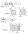
- the grating is written into the optical fibre 10 in the direction of light propagation through the fibre and, as shown in Figures 1 and 2, grating regions 11 and 12 of alternatingly high and low refractive index are formed in the optical fibre 10 with periodicity P. Also, the grating regions 11 and 12 are structured in a manner such that the amplitude of the high levels of refractive index is varied periodically with a modulation period L.
- the modulation of the amplitude might take the form of a smooth wave function or any other periodic form, but as illustrated in Figures 1 and 2 a 100% square wave modulation is applied to the grating regions so as to create spaced-apart grating portions or sections 13.
- the grating period P will typically be in the order of 0.20 to 0.60 ⁇ m, depending upon the required reflection wavelength, but will vary along the length of the grating with chirping of the grating.
- the modulation period will typically be in the order of 0.20 to 8.00 mm.
- the length of each section 13 will typically be in the order of 0.1 mm and the total grating length will typically be in the order of 5 to 10 cm.
- the grating 10 is chirped for its full length, by chirping the grating period P, the modulation period L or both the grating period and the modulation period. Which of these chirps is imposed will be dependent upon the spectral response required to be exhibited by the grating, this having been described in more detail earlier in the specification. Linear chirping is most preferably imposed on the grating, typically in the order of 0.03%.
- each of the grating sections 13 incorporates grating regions 11 and 12 of alternatingly high and low refractive index, but the grating period P within each section 13 diminishes linearly with length of the grating section.
- each grating section may be considered as being separately chirped, typically in the order of 1.0% to 5.0%, in the manner of a sample grating, but further chirping is imposed on the grating over its full length.
- the grating shown in Figures 3 and 4 will have a nominal grating period P in the order of 0.20 to 0.60 ⁇ m and will otherwise have dimensional characteristics similar to those which have been described above with reference to Figures 1 and 2.
- the grating which is shown in Figures 5 and 6 of the drawings is structured in a manner such that the phase is varied by a discontinuity in each of the successive grating sections 13.
- Each of the grating sections 13 incorporates grating regions 11 and 12 of alternatingly high and low refractive index, with a grating period P, but a phase change is introduced by interrupting the sequence of alternating high-low regions of refractive index, for example by establishing consecutive regions 11 a of high refractive index.
- Each section of the grating is identical and the sections are spaced by modulation period L.
- the grating as shown in Figures 5 and 6 has dimensional characteristics similar to those described above with reference to Figures 1 to 4.
- the grating regions of any one grating may be structured in a manner such that the amplitude and the phase, or the amplitude and the periodicity, or the phase and the periodicity are, in respective cases, both varied periodically with modulation period L.
- phase mask 14 preferably is employed in the manner indicated in Figure 7.
- the phase mask comprises a silica mask having 1 mm long parallel grooves 15 which are spaced apart with a period of 1.06 ⁇ m, assuming that the grating is to have a period P of 0.53 ⁇ m to produce a reflection peak centred on ⁇ B of 1.55 ⁇ m.
- the grooves within the phase mask are etched to a depth of approximately 240 nm, and the grooves extend over a distance of 14 cm in the direction perpendicular to their length and, thus, in the direction of propagation of light through the grating.
- the phase mask 14 may be employed to produce a grating having a 10 cm length and, with the dimensions stated, is arranged to diffract UV light at 240 nm mostly in the +1 and -1 orders of diffraction.
- the fibre 10 is stripped of its protective coating for a distance at least as long as the grating to be written (10 cm as described), and placed directly behind the phase mask 14 such that the axis of the fibre is perpendicular to the mask grooves 15.
- the fibre is laid in V-grooves 16 and is held by magnets 17, so that it is maintained under a slight tension.
- a laser beam pulsed at 10 Hz, at a wavelength of 240 nm is generated by a frequency-doubled excimer-pumped dye laser 18 and is directed through a mechanical shutter 19.
- the laser beam is deflected by a mirror 10 and focused by way of a fused silica cylindrical lens 21 which is located with its axis perpendicular to the fibre axis, in such a way that the beam width on the fibre corresponds to the width of one section 13 of the grating.
- the lens 21 has a focal length of 20 cm and the lens is positioned at a distance from the fibre selected to determine the required beam width.
- the mirror 20 and lens 21 are both mounted to a carriage 22 in such a way that they may be moved as a unit in a direction parallel to the incident laser beam and to the fibre axis.
- the focused, deflected beam from the laser is translated along the fibre by movement of the carriage 22 and is aligned in a way such as always to be incident with the same power density on the core of the fibre when the passage of the beam is unblocked by the shutter 19.
- the carriage 22 When writing the grating, the carriage 22 is first brought to rest in a desired position and the laser beam is passed through the shutter 19, so that a short section of the grating is written into the fibre as a consequence of the interference pattern created by the diffracted UV beam.
- the pulse energy of the laser beam will typically be in the order of 2 mJ, and the energy density impinging on the fibre core will typically be in the order of 10 mJ/mm 2 .
- the strength, or depth of refractive index modulation effected by the side writing is proportional to exposure time and a typical exposure time will be around 10 to 50 seconds.
- the shutter 19 is closed to block the laser beam and the carriage 22 is moved by distance L, being the period of spaced-apart sections of the grating to be written into the length of the fibre.
- the distance L is significantly greater than the period P of the grating itself and typically will be in the order of 1.00 mm.
- the distance L will be 0.812 mm by application of the formula provided earlier in this text.
- Chirping of the period P of the grating and/or of the modulation period L may be effected during formation of the grating itself by appropriately grooving the phase mask 14.
- chirping may be effected following formation of the grating, for example by use of a procedure involving application of strain differentially along the length of the grating.
- Figure 8 of the drawings shows an idealised graphical representation of the grating that is shown in Figures 1 and 2 and which is produced in the manner described above with reference to Figure 7.
- the graphical representation is applicable to a grating in which the grating period P is chirped and the modulation period L is maintained substantially constant.
- expanded reflection peaks having a spectral width ⁇ appear at each side of an expanded reflection peak that is centred on the Bragg wavelength ⁇ B , with the spacing between the peaks being ⁇ .
- the grating In the case of a grating having a centre Bragg wavelength ⁇ B of 1.55 ⁇ m and having a length in the order of 10 cm, the grating will exhibit a spectral width ⁇ B in the order of 0.01 nm and an expanded ("chirped") spectral width ⁇ in the order of 0.5 nm, resulting from a linear chirp of 0.031% applied to the grating period P over the full length of the grating.
- Figure 9 shows a plot of transmission power against wavelengths applicable to a grating that has been fabricated in a hydrogen loaded, boro-germano-silicate optical fibre.
- a 240 nm, 10 Hz, 2 mJ/pulse beam was focused to a 0.15 mm width by a cylindrical lens with its axis perpendicular to the fibre axis, in the manner described with reference to Figure 7.
- the beam was translated along the optical fibre, which was placed directly behind a 14 cm long phase mask, and translation was stopped every 1.0 mm to expose a region of the optical fibre for 40 seconds.
- the total length of the grating so produced was 100 mm and, although not shown in Figure 9, the transmission spectrum for the grating shows 15 plus strong reflection peaks with bandwidth of 0.04 nm.
- the grating was chirped following side writing to produce a linear chirp in the order of 0.03% along the full length of the grating to broaden the reflection peaks.
- Figure 9 shows a spectrum of three of the strongest peaks before and after chirping and, apart from some irregularities, attributed to deviations from linear chirp, the peaks are seen all to be broadened to the same bandwidth of 0.36 nm.
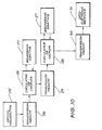
- Figure 10 shows a block diagrammatic representation of a communication system in which any one of the above described gratings may be employed for the purpose of processing multiple channels having separation ⁇ and spectral width not greater than ⁇ .
- the system includes an optical transmitter 25 in which multi-channel light outputs are generated with carrier wavelengths ⁇ 1 , ⁇ 2 ,---, ⁇ n modulated to bandwidths ⁇ 1 , ⁇ 2 ,---, ⁇ n with system information.
- the output from the transmitter 25 is launched into a first section of what is referred to generally as an optical transmission medium 26 which may include an optical fibre and such other optical components as may be required, for example, to connect, split, filter or amplify the output from the transmitter.
- a broadband grating 27 of a type as above described is located in circuit with the transmission medium 26 and the grating is selected such that it exhibits broad reflection peaks at wavelengths that coincide with each of the carrier wavelength ⁇ 1 , ⁇ 2 ,---, ⁇ n and exhibits reflection peaks having bandwidths greater than that of the bandwidths ⁇ 1 , ⁇ 2 ,---, ⁇ n .
- An optical device 28, for example in the form of a circulator or coupler, is located between the transmission medium 26 and the grating 27 for directing the transmitter output into the grating, receiving reflections from the grating and directing the reflected light into a following section of transmitting medium 29.
Landscapes
- Physics & Mathematics (AREA)
- Engineering & Computer Science (AREA)
- Manufacturing & Machinery (AREA)
- General Physics & Mathematics (AREA)
- Optics & Photonics (AREA)
- Optical Fibers, Optical Fiber Cores, And Optical Fiber Bundles (AREA)
- Diffracting Gratings Or Hologram Optical Elements (AREA)
- Optical Integrated Circuits (AREA)
Description
λB = Bragg (centre) wavelength,
n = effective (average) refractive index, and
P = grating period.
Claims (20)
- A light transmitting device (10) comprising a Bragg grating composed of grating regions (11, 12) of alternatingly high and low refractive index, the grating regions (11, 12) having periodicity P and being structured in a manner which varies periodically with a modulation period L > P, and the grating period P and/or the modulation period L being chirped over substantially the full extent of the grating,
characterised in that the grating regions are structured in a manner such that the phase of the grating regions is varied periodically with the modulation period L. - The light transmitting device as claimed in claim 1 when in the form of a length of optical fibre (10) having a core in which the grating is formed.
- The light transmitting device as claimed in claim 1 or 2 wherein, in addition to the periodic variation of the phase of the grating regions, the amplitude of the grating regions is varied periodically with the modulation period L.
- The light transmitting device as claimed in claim 1 or 2 wherein, in addition to the periodic variation of the phase of the grating regions, the grating regions are structured in a manner such that the periodicity of the grating regions is varied with the modulation period L.
- The light transmitting device as claimed in any one of the preceding claims wherein the grating period P alone is chirped over substantially the full extent of the grating and the modulation period L is maintained substantially constant whereby the grating exhibits a spectral response in which substantially identical, expanded reflection peaks appear at each side of an expanded reflection peak that is centred on the Bragg wavelength of the grating.
- The light transmitting device as claimed in any one of claims 1 to 4 wherein the modulation period L is chirped over substantially the full extent of the grating and the grating period P is maintained substantially constant whereby the grating exhibits a spectral response in which non-identical, expanded reflection peaks appear at each side of a narrow reflection peak centred on the Bragg wavelength of the grating.
- The light transmitting device as claimed in any one of claims 1 to 4 wherein the grating period P and the modulation period L are both chirped over substantially the full length of the grating whereby the grating exhibits a spectral response in which non-identical, expanded reflection peaks appear at each side of an expanded reflection peak centred on the Bragg wavelength of the grating.
- The light transmitting device as claimed in claim 3 wherein the modulation of the amplitude of the high level of the refractive index is in the form of a square wave function.
- The light transmitting device as claimed in claim 8 wherein the modulation is applied to the full refractive index depth of the grating regions whereby spaced-apart grating sections are effectively formed.
- The light transmitting device as claimed in any one of the preceding claims wherein the phase of the grating is varied periodically by introducing at least one discontinuity into each of successive sections of the length of the grating by interrupting the sequence of alternating high and low regions of the refractive index in the direction of light propagation through the grating.
- The light transmitting device as claimed in claim 4 wherein the periodicity of the grating regions is varied periodically by separately chirping each of successive sections of the grating in the direction of light propagation through the grating.
- The light transmitting device as claimed in any one of the preceding claims wherein the grating period P and/or the modulation period L is/are chirped over substantially the full extent of the grating by a linear chirp.
- A method of forming a light transmitting device (10) incorporating a Bragg grating and which comprises forming grating regions (11, 12) of alternatingly high and low refractive index with periodicity P in the direction of light propagation through the grating, structuring the grating regions in a manner which varies periodically with a modulation period L > P, and imposing chirping on either one or the other or both of the grating period P and the modulation period L over substantially the full extent of the grating,
characterised in that the phase of the grating varies periodically with modulation period L. - The method as claimed in claim 13 wherein the grating is formed within a light transmitting device in the form of an optical fibre (10).
- The method as claimed in claim 13 or claim 14 wherein, during formation of the grating regions, the amplitude of the high level of refractive index of the grating regions is modulated with the modulation period L.
- The method as claimed in claim 13 or claim 14 wherein, during formation of the grating regions, the periodicity of the grating regions is varied with the modulation period L.
- The method as claimed in any one of claims 13 to 16 wherein the chirping is applied to the grating simultaneously with formation of the grating regions.
- The method as claimed in any one of claims 13 to 16 wherein the chirping is applied to the grating subsequent to formation of the grating regions.
- An optical communication system comprising the light transmitting device as claimed in any one of claims 1 to 12, further comprising an optical transmitter (25) which is arranged to transmit light having a centre wavelength λ and bandwidth δλ, a receiver arranged to receive the transmitted light, and a light transmitting medium connecting the transmitter and the receiver, the grating being located in circuit with the light transmitting medium and the grating being selected such that one of its reflection peaks has a centre wavelength that coincides approximately with the transmitter wavelength λ and has a bandwidth at least equal to the bandwidth δλ.
- The optical communication system as claimed in claim 19, wherein the optical transmitter comprises one which is arranged to transmit multi-channel light having centre wavelengths λ1,---λn and channel bandwidths δλ1,--- ,δλn, and wherein the grating is selected such that its reflection peaks coincide approximately with the centre wavelengths λ1,---,λn and have spectral widths not less than the respective channel bandwidths δλ1,---δλn.
Applications Claiming Priority (4)
| Application Number | Priority Date | Filing Date | Title |
|---|---|---|---|
| AUPN0898A AUPN089895A0 (en) | 1995-02-03 | 1995-02-03 | Broadband grating |
| AUPN089895 | 1995-02-03 | ||
| AUPN0898/95 | 1995-02-03 | ||
| PCT/AU1996/000048 WO1996024079A1 (en) | 1995-02-03 | 1996-02-01 | Broadband grating |
Publications (3)
| Publication Number | Publication Date |
|---|---|
| EP0807271A1 EP0807271A1 (en) | 1997-11-19 |
| EP0807271A4 EP0807271A4 (en) | 1998-04-22 |
| EP0807271B1 true EP0807271B1 (en) | 2003-10-29 |
Family
ID=3785258
Family Applications (1)
| Application Number | Title | Priority Date | Filing Date |
|---|---|---|---|
| EP96901192A Expired - Lifetime EP0807271B1 (en) | 1995-02-03 | 1996-02-01 | Broadband grating |
Country Status (7)
| Country | Link |
|---|---|
| US (1) | US6081640A (en) |
| EP (1) | EP0807271B1 (en) |
| JP (1) | JPH11500539A (en) |
| AU (1) | AUPN089895A0 (en) |
| CA (1) | CA2211834A1 (en) |
| DE (1) | DE69630515D1 (en) |
| WO (1) | WO1996024079A1 (en) |
Families Citing this family (38)
| Publication number | Priority date | Publication date | Assignee | Title |
|---|---|---|---|---|
| GB2316760A (en) * | 1996-08-23 | 1998-03-04 | Univ Southampton | Fabricating optical waveguide gratings |
| US5718738A (en) | 1996-11-04 | 1998-02-17 | Lucent Technologies Inc. | Method for making continuously chirped fiber bragg gratings |
| KR100206176B1 (en) * | 1996-12-03 | 1999-07-01 | 윤종용 | Optical Attenuator and Manufacturing Method |
| JP3206536B2 (en) | 1997-02-21 | 2001-09-10 | 住友電気工業株式会社 | Semiconductor laser module |
| CA2244572A1 (en) * | 1997-08-12 | 1999-02-12 | Photonics Research Ontario | Design of complex optical fiber filters using long-period gratings |
| GB9722421D0 (en) * | 1997-10-24 | 1997-12-24 | Univ Southampton | Optical grating |
| US6915040B2 (en) | 1997-12-15 | 2005-07-05 | University Of Southern California | Devices and applications based on tunable wave-guiding bragg gratings with nonlinear group delays |
| US6453093B2 (en) * | 2000-01-07 | 2002-09-17 | Univerisity Of Southern California | Tunable optical dispersion-slope compensation based on a nonlinearly-chirped bragg grating |
| US6330383B1 (en) | 1998-02-20 | 2001-12-11 | University Of Southern California | Disperson compensation by using tunable nonlinearly-chirped gratings |
| FR2777359B1 (en) * | 1998-04-09 | 2000-07-07 | Corning Inc | CONNECTION OF OPTICAL FIBER AND OPTICAL WAVEGUIDE BY MERGER |
| KR100322121B1 (en) * | 1998-10-13 | 2002-03-08 | 윤종용 | Apparatus for fabricating long-period grating filter |
| US6563620B1 (en) * | 1999-01-25 | 2003-05-13 | Massachusetts Institute Of Technology | Quasi-dispersionless optical fiber transmission, dispersion compensation and optical clock |
| GB2346965B (en) * | 1999-02-18 | 2002-01-16 | Oxford Fiber Optic Tools Ltd | Fibre optic grating sensor |
| AUPQ300199A0 (en) * | 1999-09-21 | 1999-10-14 | University Of Sydney, The | A grating design |
| US6522808B1 (en) * | 2000-01-15 | 2003-02-18 | Corning Incorporated | System and method for writing fiber gratings and other components |
| JP2001215351A (en) * | 2000-02-04 | 2001-08-10 | Toyota Gakuen | Multi-permittivity multi-periodic structure element, its design method and manufacturing method |
| US20040033018A1 (en) * | 2000-08-07 | 2004-02-19 | Durkin Michael Kevan | Grating apodisation method and apparatus |
| US6707967B2 (en) | 2000-09-20 | 2004-03-16 | Teraxion Inc. | Efficient sampled bragg gratings for WDM applications |
| JP2002189134A (en) * | 2000-10-12 | 2002-07-05 | Matsushita Electric Ind Co Ltd | Optical wavelength filter and manufacturing method thereof |
| CN1100274C (en) * | 2000-11-06 | 2003-01-29 | 清华大学 | Flat crossed group filter |
| AUPR335901A0 (en) * | 2001-02-26 | 2001-03-22 | Redfern Optical Components Pty Ltd | Multi channel grating design |
| AUPR378901A0 (en) | 2001-03-16 | 2001-04-12 | Redfern Optical Components Pty Ltd | Grating design |
| JP3754634B2 (en) * | 2001-06-27 | 2006-03-15 | 独立行政法人科学技術振興機構 | Optical fiber grating manufacturing method and apparatus, optical fiber grating |
| NO314677B1 (en) * | 2001-06-29 | 2003-04-28 | Optoplan As | FBG production system |
| US6987908B2 (en) * | 2001-08-24 | 2006-01-17 | T-Networks, Inc. | Grating dispersion compensator and method of manufacture |
| US6654521B2 (en) | 2002-01-23 | 2003-11-25 | Teraxion Inc. | Diffraction compensation of FBG phase masks for multi-channel sampling applications |
| US6753118B2 (en) * | 2002-03-27 | 2004-06-22 | Fitel Usa Corp. | Optical grating fabrication process |
| AU2003281701B2 (en) * | 2002-07-30 | 2009-05-21 | Tyco Electronics Pty Ltd | Improved multi-channel grating design technique |
| AU2002950462A0 (en) | 2002-07-30 | 2002-09-12 | Redfern Optical Components Pty Ltd | Improved multi-channel grating design technique |
| US6788851B1 (en) | 2003-07-01 | 2004-09-07 | 3M Innovative Properties Company | Apparatus and method for adjusting the spectral response of an optical waveguide grating |
| US7006731B2 (en) * | 2003-07-01 | 2006-02-28 | 3M Innovative Properties Company | Apparatus and method for adjusting the spectral response of an optical waveguide grating |
| US6990274B2 (en) * | 2003-07-01 | 2006-01-24 | 3M Innovative Properties Company | Apparatus and method for adjusting the spectral response of an optical waveguide grating |
| US7082234B2 (en) * | 2004-08-30 | 2006-07-25 | Hojoon Lee | Wavelength division multiplexing device capable of compensating for dispersion and dispersion slope using purely phase-sampled fiber bragg grating |
| JP4657853B2 (en) * | 2005-08-11 | 2011-03-23 | 住友電工デバイス・イノベーション株式会社 | Semiconductor laser, laser module, optical component, laser device, semiconductor laser manufacturing method, and semiconductor laser control method |
| KR100782879B1 (en) * | 2006-12-07 | 2007-12-06 | 한국전자통신연구원 | Optical fiber Bragg grating manufacturing apparatus and optical fiber and mid-infrared optical fiber laser having Bragg grating manufactured by the apparatus |
| EP1962119A1 (en) * | 2007-02-20 | 2008-08-27 | Proximion Fiber Systems AB | Channelized dispersion compensation module |
| DE102015106633B4 (en) * | 2015-04-29 | 2018-05-24 | Leibniz-Institut für Photonische Technologien e. V. | Fiber-optic laser generator |
| EP3339921A1 (en) * | 2016-12-22 | 2018-06-27 | FBGS Technologies GmbH | Draw tower grating production method and system |
Family Cites Families (9)
| Publication number | Priority date | Publication date | Assignee | Title |
|---|---|---|---|---|
| US4474427A (en) * | 1979-05-07 | 1984-10-02 | Canadian Patents & Development Limited | Optical fiber reflective filter |
| US4262996A (en) * | 1979-05-29 | 1981-04-21 | Rockwell International Corporation | Chirp-grating lens for guided-wave optics |
| US4429411A (en) * | 1981-04-20 | 1984-01-31 | The United States Of America As Represented By The United States Department Of Energy | Instrument and method for focusing X-rays, gamma rays and neutrons |
| EP0192659B1 (en) * | 1984-08-13 | 1993-10-27 | United Technologies Corporation | Distributed, spatially resolving optical fiber strain gauge |
| GB8723050D0 (en) * | 1987-10-01 | 1987-11-04 | British Telecomm | Optical filters |
| US5061032A (en) * | 1989-12-26 | 1991-10-29 | United Technologies Corporation | Optical waveguide embedded light redirecting and focusing bragg grating arrangement |
| CA2137082C (en) * | 1992-06-01 | 2001-04-17 | Stephen Anthony Cassidy | Filter with preselected attenuation/wavelength characteristic |
| US5351321A (en) * | 1992-10-20 | 1994-09-27 | Elias Snitzer | Bragg grating made in optical waveguide |
| US5309260A (en) * | 1992-12-23 | 1994-05-03 | At&T Bell Laboratories | Method for forming distributed bragg reflectors in optical media |
-
1995
- 1995-02-03 AU AUPN0898A patent/AUPN089895A0/en not_active Abandoned
-
1996
- 1996-02-01 JP JP8523121A patent/JPH11500539A/en not_active Ceased
- 1996-02-01 DE DE69630515T patent/DE69630515D1/en not_active Expired - Lifetime
- 1996-02-01 EP EP96901192A patent/EP0807271B1/en not_active Expired - Lifetime
- 1996-02-01 US US08/875,502 patent/US6081640A/en not_active Expired - Lifetime
- 1996-02-01 WO PCT/AU1996/000048 patent/WO1996024079A1/en not_active Ceased
- 1996-02-01 CA CA002211834A patent/CA2211834A1/en not_active Abandoned
Also Published As
| Publication number | Publication date |
|---|---|
| WO1996024079A1 (en) | 1996-08-08 |
| AUPN089895A0 (en) | 1995-03-02 |
| EP0807271A1 (en) | 1997-11-19 |
| CA2211834A1 (en) | 1996-08-08 |
| JPH11500539A (en) | 1999-01-12 |
| DE69630515D1 (en) | 2003-12-04 |
| US6081640A (en) | 2000-06-27 |
| EP0807271A4 (en) | 1998-04-22 |
Similar Documents
| Publication | Publication Date | Title |
|---|---|---|
| EP0807271B1 (en) | Broadband grating | |
| US20020105727A1 (en) | Fabricating optical waveguide gratings | |
| EP0866989B1 (en) | Formation of a refractive index grating | |
| US6002822A (en) | Article comprising an optional waveguide tap | |
| CA2119045C (en) | Optical waveguiding component comprising a band-pass filter | |
| EP0221560B1 (en) | Coupling device for single mode optical fiber and communications system comprising same | |
| US5764829A (en) | Optical signal shaping device for complex spectral shaping applications | |
| RU2141679C1 (en) | Optical attenuator and method for its manufacturing | |
| EP0684493A2 (en) | Wavelength division optical multiplexing elements | |
| US4912523A (en) | Optical fiber communication system comprising mode-stripping means | |
| EP1177470A1 (en) | Dispersion compensation by using tunable nonlinearly-chirped gratings | |
| EP0777347B1 (en) | Optical transmission system and optical repeater | |
| US6865319B2 (en) | Optical structure for the compensation of chromatic dispersion in a light signal | |
| EP0947864B1 (en) | Broadband long-period gratings | |
| AU728818B2 (en) | Optical dispersion compensation | |
| Hill et al. | Aperiodic in-fiber Bragg gratings for optical fiber dispersion compensation | |
| Petruzzi et al. | Dispersion compensation using only fiber Bragg gratings | |
| AU693641B2 (en) | Broadband grating | |
| EP1216427A1 (en) | A grating design | |
| Li et al. | Multi-channel high-performance tunable dispersion compensator for 40 Gb/s transmission systems | |
| Ezilarasan et al. | Implementation of Fiber Bragg Grating for Dispersion Loss Compensation in Optical Fiber Communication | |
| US20040252944A1 (en) | Apparatus and method of manufacturing optical waveguide type diffraction grating device | |
| Sabharwal | Fiber Bragg gratings: Application to dispersion compensation | |
| GB2320828A (en) | Isolated multiple grating system for filtering | |
| JP2008058694A (en) | Fiber Bragg Grating Element, Fiber Bragg Grating Element Manufacturing Method and Manufacturing Apparatus |
Legal Events
| Date | Code | Title | Description |
|---|---|---|---|
| PUAI | Public reference made under article 153(3) epc to a published international application that has entered the european phase |
Free format text: ORIGINAL CODE: 0009012 |
|
| 17P | Request for examination filed |
Effective date: 19970804 |
|
| AK | Designated contracting states |
Kind code of ref document: A1 Designated state(s): DE FR GB IT |
|
| A4 | Supplementary search report drawn up and despatched |
Effective date: 19980305 |
|
| AK | Designated contracting states |
Kind code of ref document: A4 Designated state(s): DE FR GB IT |
|
| 17Q | First examination report despatched |
Effective date: 20020405 |
|
| GRAH | Despatch of communication of intention to grant a patent |
Free format text: ORIGINAL CODE: EPIDOS IGRA |
|
| GRAH | Despatch of communication of intention to grant a patent |
Free format text: ORIGINAL CODE: EPIDOS IGRA |
|
| GRAA | (expected) grant |
Free format text: ORIGINAL CODE: 0009210 |
|
| AK | Designated contracting states |
Kind code of ref document: B1 Designated state(s): DE FR GB IT |
|
| PG25 | Lapsed in a contracting state [announced via postgrant information from national office to epo] |
Ref country code: IT Free format text: LAPSE BECAUSE OF FAILURE TO SUBMIT A TRANSLATION OF THE DESCRIPTION OR TO PAY THE FEE WITHIN THE PRESCRIBED TIME-LIMIT;WARNING: LAPSES OF ITALIAN PATENTS WITH EFFECTIVE DATE BEFORE 2007 MAY HAVE OCCURRED AT ANY TIME BEFORE 2007. THE CORRECT EFFECTIVE DATE MAY BE DIFFERENT FROM THE ONE RECORDED. Effective date: 20031029 Ref country code: FR Free format text: LAPSE BECAUSE OF FAILURE TO SUBMIT A TRANSLATION OF THE DESCRIPTION OR TO PAY THE FEE WITHIN THE PRESCRIBED TIME-LIMIT Effective date: 20031029 |
|
| REG | Reference to a national code |
Ref country code: GB Ref legal event code: FG4D |
|
| REF | Corresponds to: |
Ref document number: 69630515 Country of ref document: DE Date of ref document: 20031204 Kind code of ref document: P |
|
| PGFP | Annual fee paid to national office [announced via postgrant information from national office to epo] |
Ref country code: GB Payment date: 20040128 Year of fee payment: 9 |
|
| PG25 | Lapsed in a contracting state [announced via postgrant information from national office to epo] |
Ref country code: DE Free format text: LAPSE BECAUSE OF FAILURE TO SUBMIT A TRANSLATION OF THE DESCRIPTION OR TO PAY THE FEE WITHIN THE PRESCRIBED TIME-LIMIT Effective date: 20040130 |
|
| PLBE | No opposition filed within time limit |
Free format text: ORIGINAL CODE: 0009261 |
|
| STAA | Information on the status of an ep patent application or granted ep patent |
Free format text: STATUS: NO OPPOSITION FILED WITHIN TIME LIMIT |
|
| 26N | No opposition filed |
Effective date: 20040730 |
|
| EN | Fr: translation not filed | ||
| PG25 | Lapsed in a contracting state [announced via postgrant information from national office to epo] |
Ref country code: GB Free format text: LAPSE BECAUSE OF NON-PAYMENT OF DUE FEES Effective date: 20050201 |
|
| GBPC | Gb: european patent ceased through non-payment of renewal fee |
Effective date: 20050201 |