EP0805539A1 - Schaltungsanordnung für ein Hochspannungsdrehstromkabel - Google Patents
Schaltungsanordnung für ein Hochspannungsdrehstromkabel Download PDFInfo
- Publication number
- EP0805539A1 EP0805539A1 EP96110589A EP96110589A EP0805539A1 EP 0805539 A1 EP0805539 A1 EP 0805539A1 EP 96110589 A EP96110589 A EP 96110589A EP 96110589 A EP96110589 A EP 96110589A EP 0805539 A1 EP0805539 A1 EP 0805539A1
- Authority
- EP
- European Patent Office
- Prior art keywords
- voltage
- node
- circuit
- resistors
- delay
- Prior art date
- Legal status (The legal status is an assumption and is not a legal conclusion. Google has not performed a legal analysis and makes no representation as to the accuracy of the status listed.)
- Granted
Links
- 239000004020 conductor Substances 0.000 abstract description 2
- 238000005265 energy consumption Methods 0.000 description 8
- 230000001681 protective effect Effects 0.000 description 4
- XLOMVQKBTHCTTD-UHFFFAOYSA-N Zinc monoxide Chemical compound [Zn]=O XLOMVQKBTHCTTD-UHFFFAOYSA-N 0.000 description 2
- 239000003990 capacitor Substances 0.000 description 2
- 238000010521 absorption reaction Methods 0.000 description 1
- 238000004364 calculation method Methods 0.000 description 1
- 238000005094 computer simulation Methods 0.000 description 1
- 238000011161 development Methods 0.000 description 1
- 230000018109 developmental process Effects 0.000 description 1
- 230000005611 electricity Effects 0.000 description 1
- 238000004088 simulation Methods 0.000 description 1
- 239000011787 zinc oxide Substances 0.000 description 1
Images
Classifications
-
- H—ELECTRICITY
- H02—GENERATION; CONVERSION OR DISTRIBUTION OF ELECTRIC POWER
- H02H—EMERGENCY PROTECTIVE CIRCUIT ARRANGEMENTS
- H02H7/00—Emergency protective circuit arrangements specially adapted for specific types of electric machines or apparatus or for sectionalised protection of cable or line systems, and effecting automatic switching in the event of an undesired change from normal working conditions
- H02H7/22—Emergency protective circuit arrangements specially adapted for specific types of electric machines or apparatus or for sectionalised protection of cable or line systems, and effecting automatic switching in the event of an undesired change from normal working conditions for distribution gear, e.g. bus-bar systems; for switching devices
- H02H7/228—Emergency protective circuit arrangements specially adapted for specific types of electric machines or apparatus or for sectionalised protection of cable or line systems, and effecting automatic switching in the event of an undesired change from normal working conditions for distribution gear, e.g. bus-bar systems; for switching devices for covered wires or cables
-
- H—ELECTRICITY
- H01—ELECTRIC ELEMENTS
- H01B—CABLES; CONDUCTORS; INSULATORS; SELECTION OF MATERIALS FOR THEIR CONDUCTIVE, INSULATING OR DIELECTRIC PROPERTIES
- H01B9/00—Power cables
- H01B9/02—Power cables with screens or conductive layers, e.g. for avoiding large potential gradients
- H01B9/029—Screen interconnecting circuits
-
- H—ELECTRICITY
- H02—GENERATION; CONVERSION OR DISTRIBUTION OF ELECTRIC POWER
- H02G—INSTALLATION OF ELECTRIC CABLES OR LINES, OR OF COMBINED OPTICAL AND ELECTRIC CABLES OR LINES
- H02G15/00—Cable fittings
- H02G15/08—Cable junctions
- H02G15/10—Cable junctions protected by boxes, e.g. by distribution, connection or junction boxes
- H02G15/103—Cable junctions protected by boxes, e.g. by distribution, connection or junction boxes with devices for relieving electrical stress
- H02G15/105—Cable junctions protected by boxes, e.g. by distribution, connection or junction boxes with devices for relieving electrical stress connected to the cable shield only
- H02G15/1055—Cable junctions protected by boxes, e.g. by distribution, connection or junction boxes with devices for relieving electrical stress connected to the cable shield only with cross-bonding of cable shields
-
- H—ELECTRICITY
- H02—GENERATION; CONVERSION OR DISTRIBUTION OF ELECTRIC POWER
- H02H—EMERGENCY PROTECTIVE CIRCUIT ARRANGEMENTS
- H02H7/00—Emergency protective circuit arrangements specially adapted for specific types of electric machines or apparatus or for sectionalised protection of cable or line systems, and effecting automatic switching in the event of an undesired change from normal working conditions
- H02H7/008—Emergency protective circuit arrangements specially adapted for specific types of electric machines or apparatus or for sectionalised protection of cable or line systems, and effecting automatic switching in the event of an undesired change from normal working conditions for protective arrangements according to this subclass
Definitions
- the invention relates to a circuit arrangement according to the preamble of the main claim (cross-bonding circuit).
- a resistor can normally be protected by connecting one or more resistors in parallel to a resistor that is endangered by overcurrent, because it is no longer the total current that flows through one resistor, but only part of the current distribution.
- the invention is intended to provide a circuit arrangement which in the event of voltage spikes prevents or reduces damage to non-linear protective resistors of a cross-bonding circuit.
- the crucial proposal is to provide a kind of 'energy redirection' through which partial energy transfer takes place at the nodes. It is essential in the division that there is a time delay in the current supply to the additional non-linear resistors.
- This solution has the advantage that the circuit does not have to be provided with primary non-linear resistors that are designed for the maximum possible power. The performance cannot be increased arbitrarily. If the protective effect of the resistors also comes into play in the rare cases in which a critical voltage surge occurs, they would have to be oversized.
- the appropriate use of some components according to the invention - which can furthermore also only have a reduced energy absorption capacity - creates a cost advantage in any case.
- the wave resistance of the delay element has a decisive influence on the energy deflection.
- the more energy that is to be kept away from the primary nonlinear resistor the smaller the wave resistance or the wave resistances of the delay line or the more parallel delay lines have to be provided.
- the characteristic size of the delay (e.g. the length of the delay line) has a noticeable influence on the energy distribution. If the delay (length of the line) is zero, all of the energy goes into the primary resistance or resistances at the node. But if the delay is infinite, no energy goes into the additional resistors.
- each node one or more delay lines are connected, at the opposite ends of which a voltage-limiting component is connected to ground, the response voltage of the further voltage-limiting components and / or the characteristic impedance of the associated delay elements being as large as the response voltage of the primary resistor and / or the characteristic impedance of the respectively associated delay elements can be chosen to be the same.
- the response voltage is cheaper the other voltage-limiting components to be chosen smaller than that of the primary resistor.
- the optimal solution is found by a suitable combination of the four parameters response voltage, characteristic impedance and delay time of a delay element and number of delay lines.
- the response voltage of the first further non-linear resistor can be reduced to 9 kV and that of the second further non-linear resistor to 7 kV.
- the characteristic impedance of the associated lines can be reduced by the same amount or staggered in relation to the power consumption of the resistors.
- a line used as a delay element should preferably be designed so that it has a length in the range of 1 to 10 meters and a characteristic impedance of 20 to 150 ohms / m.
- the known zinc oxide resistors can be selected as voltage-limiting components.
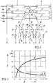
- Fig. 1 shows schematically a three-phase cable with its three conductors 100,200,300.
- the shields 1, 2, 3 are grounded at point K0.
- the screens 1, 2, 3 and 1 ', 2', 3 ' are crossed out to one another.
- non-linear resistors 10, 11, 12 are connected to ground.
- the critical voltage is present at the nodes K1, K2, K3.
- two further non-linear resistors are in series with a delay line L10, L11, L20, L21, L30, at the nodes K1, K2, K3.
- L31 connected in parallel. For example, not only the non-linear resistor 11 but also the two delay lines L20 and L21, which lead via the points b1, b2 to the further, grounded non-linear resistors 21, 31, are thus at the node K2.
- non-linear resistors (20, 21, 22, 30, 31, 32) and their associated lines (L10, L20, L30, L11, L21, L31) connected to the primary non-linear resistor 10, 11 or 12 of a cross-bonding circuit. is shown in Fig. 1 only as an example with two each. Depending on the design of the circuit arrangement, only one further non-linear resistor with associated delay line, but also more than two non-linear resistors with line, can be located at a node K1, K2, K3.
- FIG. 2 shows the energy consumption E of the non-linear resistors at a node from a computational simulation. It is also said that maximum energy consumption of non-linear resistors is of the order of 30 kWs.
- a capacitor with a charging voltage of 500 kV was selected, which is discharged after 80 microseconds if it is connected to the primary non-linear resistor, a primary non-linear resistor (10) with 11 kV and two secondary non-linear resistors (20, 30 ) with 9 kV voltage limitation.
- the secondary resistors (20, 30) each have a delay line (L10, L11) of 3 meters in length at the node (K1). Shown in FIG.
- the characteristic curve 1 belongs to the primary resistor 10 and the characteristic curves 2 and 3 belong to the two resistors 20 and 30 of the delay lines L10, L11.
- the wave resistances Z of the delay lines have a great influence on the energy deflection.
- a calculation of the energy consumption depending on the length of the delay line corresponding to FIG. 2 provides a similar situation.
- the energy consumption of the primary resistor 10 would remain below 30 kWs if the length of the lines L10, L11 were chosen to be less than or equal to 3 meters.
Landscapes
- Emergency Protection Circuit Devices (AREA)
- Communication Cables (AREA)
Abstract
Description
- Die Erfindung betrifft eine Schaltungsanordnung nach dem Oberbegriff des Hauptanspruchs (Crossbonding-Beschaltung).
- Bei Spannungsüberhöhungen, beispielsweise durch Resonanzerscheinungen, kann es zu Kurzschlüssen kommen, bei denen einige oder auch alle nichtlinearen Schutzwiderstände der Crossbonding-Beschaltung wegen zu hoher Energieaufnahme zerstört werden können. Im folgenden werden die Punkte in einer Crossbonding-Beschaltung, an denen nichtlineare Schutzwiderstände liegen, mit Knotenpunkte bezeichnet. Durch eine Parallelschaltung einer oder mehrerer Widerstände zu einem durch Überstrom gefährdeten Widerstand kann normalerweise ein Widerstand geschützt werden, weil nicht mehr der Gesamtstrom durch den einen Widerstand fließt, sondern durch die Stromaufteilung nur noch ein Teil. Diese Maßnahme der Stromaufteilung ist für nichtlineare Widerstände und damit für eine Crossbonding-Beschaltung nicht geeignet, da auch nur kleinste Unterschiede in der Ansprechspannung bewirken, daß derjenige Widerstand mit der kleinsten Ansprechspannung den gesamten Strom übernimmt und zerstört wird, ohne daß die parallel geschalteten Widerstände merklich Strom führen.
- Mit der Erfindung soll eine Schaltungsanordnung angegeben werden, die im Falle von Spannungsüberhöhungen Schäden an nichtlinearen Schutzwiderständen einer Crossbonding-Beschaltung abwendet bzw. verringert.
- Die Lösung findet sich in den Merkmalen des Hauptanspruchs. Vorteilhafte Weiterbildungen sind in den Unteransprüchen angegeben.
- Der entscheidende Vorschlag liegt darin, eine Art 'Energieumlenkung' vorzusehen, durch die eine teilweise Energiefortleitung an den Knotenpunkten stattfindet. Bei der Aufteilung ist wesentlich, daß eine zeitliche Verzögerung der Stromzufuhr zu den zusätzlichen nichtlinearen Widerständen stattfindet. Diese Lösung hat den Vorteil, daR die Schaltung nicht mit primären nichtlinearen Widerständen versehen werden muß, die für die maximal mögliche Leistung ausgelegt sind. Das Leistungsvermögen ist nicht beliebig steigerbar. Sollte die schützende Wirkung der Widerstände auch in den seltenen Fällen zum Tragen kommen, in denen eine kritische Spannungsüberhöhung auftritt, müßten sie überdimensioniert werden. Durch die geeignete Verwendung einiger Bauelemente gemäß der Erfindung - die zum weiteren auch nur verringertes Energieaufnahmevermögen haben können - entsteht auf jeden Fall ein Kostenvorteil.
- Der Wellenwiderstand des Verzögerungsglieds hat entscheidenden Einfluß auf die Energieumlenkung. Für den einfachen Fall, in dem als Verzögerungsglied eine Verzögerungsleitung eingesetzt wird, heißt dies, daß die Länge der Leitung und/oder ihr Wellenwiderstand wesentlich sind.
- Je mehr Energie vom primären nichtlinearen Widerstand ferngehalten werden soll, desto kleiner müssen der oder die Wellenwiderstände der Verzögerungsleitung sein oder umso mehr parallel liegende Verzögerungsleitungen müssen vorgesehen werden.
- Die charakteristische Größe der Verzögerung (z.B. die Länge der Verzögerungsleitung) hat einen spürbaren Einfluß auf die Energieaufteilung. Ist nämlich die Verzögerung (Länge der Leitung) Null, geht die gesamte Energie in den oder die primären Widerstände am Knotenpunkt. Ist aber die Verzögerung unendlich groß, geht keine Energie in die Zusatzwiderstände.
- In jedem Knotenpunkt sind jeweils eine oder mehrere Verzögerungsleitungen angeschaltet, an deren abgewandten Enden jeweils ein spannungsbegrenzendes Bauelement gegen Masse geschaltet ist, wobei die Ansprechspannung der weiteren spannungsbegrenzenden Bauelemente und/oder der Wellenwiderstand der jeweils zugehörigen Verzögerungsglieder so groß wie die Ansprechspannung des primären Widerstands und/oder der Wellenwiderstand der jeweils zugehörigen Verzögerungsglieder untereinander gleich groß gewählt werden kann. Günstiger ist es jedoch, die Ansprechspannung der weiteren spannungsbegrenzenden Bauelemente kleiner als die des primären Widerstands zu wählen. Die optimale Lösung wird durch geeignete Kombination der vier Parameter Ansprechspannung, Wellenwiderstand und Laufzeit eines Verzögerungsglieds und Zahl der Verzögerungsleitungen gefunden.
- Beispielsweise kann bei einer Crossbonding-Beschaltung mit primären nichtlinearen Widerständen mit 11 kV Ansprechspannung die Ansprechspannung des ersten weiteren nichtlinearen Widerstands auf 9 kV und die des zweiten weiteren nichtlinearen Widerstands auf 7 kV reduziert werden. Der Wellenwiderstand der zugehörigen Leitungen kann untereinader gleich oder auch im Verhältnis wie die Leistungsaufnahme der Widerstände gestaffelt verringert werden.
- Eine als Verzögerungsglied eingesetzte Leitung sollte vorzugsweise so ausgelegt sein, daß sie eine Länge im Bereich von 1 bis 10 Metern und einen Wellenwiderstand von 20 bis 150 Ohm/m hat.
- Als spannungsbegrenzende Bauelemente können die bekannten Zink-Oxid-Widerstände gewählt werden.
- Die Erfindung ist in zwei Figuren dargestellt. Es zeigen
- Fig. 1 die Schaltungsanordnung und
- Fig. 2 die Verhältnisse der Energieaufnahme.
- Fig. 1 zeigt schematisch ein Drehstromkabel mit seinen drei Leitern 100,200,300. Am Punkt K0 sind die Schirme 1,2,3 geerdet. Die Schirme 1,2, 3 und 1',2',3' sind ausgekreuzt miteinander verbunden. An den Knotenpunkten K1,K2,K3 sind nichtlineare Widerstände 10,11,12 gegen Masse hinzugeschaltet. An den Knotenpunkten K1,K2,K3 steht bei Spannungsüberhöhung die kritische Spannung an. Um die Energie so abführen zu können, daß die nichtlinearen Widerstände 10,11,12 nicht zerstört werden, sind an den Knotenpunkten K1,K2,K3 jeweils zwei weitere nichtlineare Widerstände in Reihe mit einer Verzögerungsleitung L10,L11,L20, L21,L30,L31 parallel geschaltet. Beispielsweise liegen damit am Knotenpunkt K2 nicht nur der nichtlineare Widerstand 11 sondern auch die beiden Verzögerungsleitungen L20 und L21, die über die Punkte b1,b2 zu den weiteren, geerdeten nichtlinearen Widerständen 21,31 führen.
- Die Zahl der jeweils zum primären nichtlinearen Widerstand 10, 11 oder 12 einer Crossbonding-Beschaltung hinzugeschaltenen nichtlinearen Widerstände (20,21,22,30,31,32) und deren zugehörige Leitungen (L10,L20,L30,L11,L21,L31) ist in Fig. 1 nur beispielhaft mit je zwei dargestellt. Je nach Auslegung der Schaltungsanordnung können an einem Knotenpunkt K1,K2,K3 auch nur ein weiterer nichtlinearer Widerstand mit zugehöriger Verzögerungsleitung aber auch mehr als zwei nichtlineare Widerstände mit Leitung liegen.
- In Fig. 2 ist die Energieaufnahme E der nichtlinearen Widerstände an einem Knotenpunkt aus einer rechnerischen Simulation dargestellt. Vorausgeschickt wird noch, daß maximale Energieaufnahmen von nichtlinearen Widerständen in der Größenordnung von 30 kWs liegen. Bei der Simulation wurde ein Kondensator mit einer Ladespannung von 500 kV gewählt, der nach 80 Mikrosekunden entladen ist, falls er an den primären nichtlinearen Widerstand geschaltet wird, ein primärer nichtlinearen Widerstand (10) mit 11 kV und zwei sekundäre nichtlineare Widerstände (20, 30) mit 9 kV Spannungsbegrenzung. Die sekundären Widerstände (20,30) liegen mit je einer Verzögerungsleitung (L10,L11) von 3 Meter Länge am Knotenpunkt (K1). Dargestellt in der Fig. 2 ist die Energieaufnahme nach der Entladezeit des Kondensators als Funktion des Wellenwiderstands Z der Leitungen L10,L11. Die Kennlinie 1 gehört zum primären Widerstand 10 und die Kennlinien 2 und 3 gehören zu den beiden Widerständen 20 und 30 der Verzögerungsleitungen L10, L11.
- Aus der Fig. 2 ist zu entnehmen, daß die Wellenwiderstände Z der Verzögerungsleitungen einen großen Einfluß auf die Energieumlenkung haben. Je mehr Energie vom primären Widerstand 10 ferngehalten werden soll, desto kleiner müssen die Wellenwiderstände der Verzögerungsleitungen L10,L11 sein. Soll also die Energieaufnahme des Widerstands 10 30 kWs nicht überschreiten, muß der Wellenwiderstand der Verzögerungsleitung zu etwa 100 Ohm (oder kleiner) gewählt werden.
- Eine der Fig. 2 entsprechende Berechnung der Energieaufnahme in Abhängigkeit der Länge der Verzögerungsleitung liefert einen ähnlichen Sachverhalt. So würde bei einem Wellenwiderstand von 100 Ohm der Verzögerungsleitungen L10,L11 die Energieaufnahme des primären Widerstands 10 unter 30 kWs begrenzt bleiben, wenn die Länge der Leitungen L10,L11 kleiner oder gleich 3 Meter gewählt werden würde.
Claims (3)
- Schaltungsanordnung für ein Hochspannungsdrehstromkabel bestehend aus Einleiterkabeln, deren Mäntel oder Schirme (1,2,3,1',2',3') an mindestens einem Punkt (K0) ihrer Längen geerdet und an mindestens einem weiteren Punkt (hier 'Knotenpunkt' genannt) (K1,K2,K3) untereinander verbunden und über spannungsbegrenzende Bauelemente (10,11,12) geerdet sind (Crossbonding-Beschaltung), dadurch gekennzeichnet,
daß in jedem Knotenpunkt (K1,K2,K3) mindestens ein weiteres spannungsbegrenzendes Bauelement (20,21,22) in Reihe mit einem Verzögerungsglied (L10,L20,L30) gegen Masse geschaltet ist. - Schaltungsanordnung nach Anspruch 1, dadurch gekennzeichnet, daß das Verzögerungsglied (L10,L20,L30) am Knotenpunkt (K1,K2,K3) und das spannungsbegrenzende Bauelement (20,21,22) in Reihe dahinter liegt.
- Schaltungsanordnung nach einem der Ansprüche 1 oder 2, dadurch gekennzeichnet, daß in jedem Knotenpunkt (K1,K2,K3) jeweils mehrere in Reihe mit einem Verzögerungsglied (L10,L20,L30) liegende, spannungsbegrenzende Bauelemente (20,30,21,31,22,32) gegen Masse geschaltet sind, wobei die Ansprechspannung der weiteren spannungsbegrenzenden Bauelemente (20,30,21,31,22,32) kleiner ist als die des primären spannungsbegrenzenden Bauelements (10,11,12).
Applications Claiming Priority (2)
| Application Number | Priority Date | Filing Date | Title |
|---|---|---|---|
| DE19617485 | 1996-05-02 | ||
| DE19617485 | 1996-05-02 |
Publications (2)
| Publication Number | Publication Date |
|---|---|
| EP0805539A1 true EP0805539A1 (de) | 1997-11-05 |
| EP0805539B1 EP0805539B1 (de) | 1999-05-12 |
Family
ID=7793023
Family Applications (1)
| Application Number | Title | Priority Date | Filing Date |
|---|---|---|---|
| EP96110589A Expired - Lifetime EP0805539B1 (de) | 1996-05-02 | 1996-07-01 | Schaltungsanordnung für ein Hochspannungsdrehstromkabel |
Country Status (4)
| Country | Link |
|---|---|
| EP (1) | EP0805539B1 (de) |
| AT (1) | ATE180114T1 (de) |
| DE (1) | DE59601877D1 (de) |
| DK (1) | DK0805539T3 (de) |
Cited By (1)
| Publication number | Priority date | Publication date | Assignee | Title |
|---|---|---|---|---|
| DE102004040247A1 (de) * | 2004-08-13 | 2006-02-23 | Siemens Ag | Elektroenergieübertragungseinrichtung mit einem Phasenleiter und einem Mantelleiter |
Citations (1)
| Publication number | Priority date | Publication date | Assignee | Title |
|---|---|---|---|---|
| US4464583A (en) * | 1983-03-04 | 1984-08-07 | Mcgraw-Edison Company | Apparatus for bonding and protecting electrical cable shields |
-
1996
- 1996-07-01 DE DE59601877T patent/DE59601877D1/de not_active Expired - Fee Related
- 1996-07-01 AT AT96110589T patent/ATE180114T1/de not_active IP Right Cessation
- 1996-07-01 DK DK96110589T patent/DK0805539T3/da active
- 1996-07-01 EP EP96110589A patent/EP0805539B1/de not_active Expired - Lifetime
Patent Citations (1)
| Publication number | Priority date | Publication date | Assignee | Title |
|---|---|---|---|---|
| US4464583A (en) * | 1983-03-04 | 1984-08-07 | Mcgraw-Edison Company | Apparatus for bonding and protecting electrical cable shields |
Non-Patent Citations (1)
| Title |
|---|
| LEUFKENS P P ET AL: "Cross bonding and a special interruption joint for HV XLPE cable in relation with the use of metal oxide surge arresters", CIGRE. PROCEEDINGS OF THE 32ND SESSION. INTERNATIONAL CONFERENCE ON LARGE HIGH VOLTAGE ELECTRIC SYSTEMS, PARIS, FRANCE, 28 AUG.-3 SEPT. 1988, 1988, PARIS, FRANCE, CIGRE, FRANCE, pages 21 - 04/1-5 vol.1, XP000041993 * |
Cited By (1)
| Publication number | Priority date | Publication date | Assignee | Title |
|---|---|---|---|---|
| DE102004040247A1 (de) * | 2004-08-13 | 2006-02-23 | Siemens Ag | Elektroenergieübertragungseinrichtung mit einem Phasenleiter und einem Mantelleiter |
Also Published As
| Publication number | Publication date |
|---|---|
| ATE180114T1 (de) | 1999-05-15 |
| EP0805539B1 (de) | 1999-05-12 |
| DE59601877D1 (de) | 1999-06-17 |
| DK0805539T3 (da) | 1999-11-01 |
Similar Documents
| Publication | Publication Date | Title |
|---|---|---|
| DE60115248T2 (de) | Überspannungsschutzsystem | |
| EP0855758A1 (de) | Schaltungsanordnung zum Schutz von HF-Eingangskreisen von Telekommunikationsgeräten | |
| DE2728703A1 (de) | Anschlussvorrichtung fuer eine fernsprechverteiler-einrichtung | |
| DE69415379T2 (de) | Überspannungsschutzschaltung | |
| AT504439A4 (de) | Schaltungsanordnung mit wenigstens zwei in serie geschalteten kondensatoren | |
| EP0092052B1 (de) | Anordnung zum Schutz von an Leitungen angeschlossenen Geräten vor Über- oder Störspannungen | |
| EP2128941B1 (de) | Überspannungsschutzgerät | |
| EP0968628A1 (de) | Aktive entladeelektrode zum minimieren von positiven und/oder negativen ladungen auf bewegten materialbahnen | |
| WO2016008919A1 (de) | Reihenklemmsystem | |
| EP0980003A1 (de) | RC-Spannungsteiler | |
| EP0561149A2 (de) | Anordnung zur Stromversorgung einer Elektronik aus einem Drehstromnetz | |
| EP0805539B1 (de) | Schaltungsanordnung für ein Hochspannungsdrehstromkabel | |
| DE3611793A1 (de) | Ueberspannungsschutzeinrichtung fuer elektrische anlagen, insbesondere fuer elektronische apparate | |
| DE202008012738U1 (de) | Reihenschluss-Überspannungsbegrenzer | |
| DE3027469A1 (de) | Blitzschutz von transportablen fernmelde-betriebsstellen | |
| DE1922814A1 (de) | Funkenstreckenanordnung fuer UEberschlagssicherung | |
| DE2342772C3 (de) | Hochspannungshalbleitergleichrichter | |
| DE212023000198U1 (de) | Vorrichtung zum Schützen einer Messschaltung | |
| DE4236584A1 (en) | Overload voltage protector e.g. for use with control and instrumentation equipment - has modular structure with overload elements in housing interconnected by bridging strips. | |
| DE2753171A1 (de) | Vorrichtung zum schutz elektrischer, insbesondere fernmeldetechnischer anlagen gegen ueberspannungsimpulse | |
| AT397439B (de) | Schaltung zur überwachung der isolationswiderstände einer schar von baugruppen einer elektrischen anlage mit gemeinsamer erdfreier stromversorgung, insbesondere einer fernmelde- oder signaltechnischen einrichtung | |
| DE3012741A1 (de) | Ueberspannungsableiter mit einer saeule von ableiterelementen und abschirmkoerpern | |
| DE2248113C3 (de) | Überspannungsableiter mit gesonderten Steuereinheiten | |
| EP0806826B1 (de) | Entkoppelglied für Überspannungsschutz-Schaltung | |
| DE9116301U1 (de) | Überspannungs-Schutzgerät für Datenkabel |
Legal Events
| Date | Code | Title | Description |
|---|---|---|---|
| PUAI | Public reference made under article 153(3) epc to a published international application that has entered the european phase |
Free format text: ORIGINAL CODE: 0009012 |
|
| AK | Designated contracting states |
Kind code of ref document: A1 Designated state(s): AT DE DK GB IE NL |
|
| 17P | Request for examination filed |
Effective date: 19980811 |
|
| GRAG | Despatch of communication of intention to grant |
Free format text: ORIGINAL CODE: EPIDOS AGRA |
|
| RAP1 | Party data changed (applicant data changed or rights of an application transferred) |
Owner name: FELTEN & GUILLEAUME AG |
|
| GRAG | Despatch of communication of intention to grant |
Free format text: ORIGINAL CODE: EPIDOS AGRA |
|
| GRAH | Despatch of communication of intention to grant a patent |
Free format text: ORIGINAL CODE: EPIDOS IGRA |
|
| 17Q | First examination report despatched |
Effective date: 19981102 |
|
| GRAH | Despatch of communication of intention to grant a patent |
Free format text: ORIGINAL CODE: EPIDOS IGRA |
|
| GRAA | (expected) grant |
Free format text: ORIGINAL CODE: 0009210 |
|
| AK | Designated contracting states |
Kind code of ref document: B1 Designated state(s): AT DE DK GB IE NL |
|
| REF | Corresponds to: |
Ref document number: 180114 Country of ref document: AT Date of ref document: 19990515 Kind code of ref document: T |
|
| REG | Reference to a national code |
Ref country code: IE Ref legal event code: FG4D Free format text: GERMAN |
|
| REF | Corresponds to: |
Ref document number: 59601877 Country of ref document: DE Date of ref document: 19990617 |
|
| GBT | Gb: translation of ep patent filed (gb section 77(6)(a)/1977) |
Effective date: 19990628 |
|
| REG | Reference to a national code |
Ref country code: DK Ref legal event code: T3 |
|
| PLBE | No opposition filed within time limit |
Free format text: ORIGINAL CODE: 0009261 |
|
| STAA | Information on the status of an ep patent application or granted ep patent |
Free format text: STATUS: NO OPPOSITION FILED WITHIN TIME LIMIT |
|
| 26N | No opposition filed | ||
| REG | Reference to a national code |
Ref country code: GB Ref legal event code: IF02 |
|
| PGFP | Annual fee paid to national office [announced via postgrant information from national office to epo] |
Ref country code: IE Payment date: 20040622 Year of fee payment: 9 |
|
| PGFP | Annual fee paid to national office [announced via postgrant information from national office to epo] |
Ref country code: GB Payment date: 20050621 Year of fee payment: 10 |
|
| PGFP | Annual fee paid to national office [announced via postgrant information from national office to epo] |
Ref country code: AT Payment date: 20050628 Year of fee payment: 10 |
|
| PG25 | Lapsed in a contracting state [announced via postgrant information from national office to epo] |
Ref country code: IE Free format text: LAPSE BECAUSE OF NON-PAYMENT OF DUE FEES Effective date: 20050701 |
|
| PGFP | Annual fee paid to national office [announced via postgrant information from national office to epo] |
Ref country code: NL Payment date: 20050714 Year of fee payment: 10 Ref country code: DK Payment date: 20050714 Year of fee payment: 10 Ref country code: DE Payment date: 20050714 Year of fee payment: 10 |
|
| REG | Reference to a national code |
Ref country code: IE Ref legal event code: MM4A |
|
| PG25 | Lapsed in a contracting state [announced via postgrant information from national office to epo] |
Ref country code: GB Free format text: LAPSE BECAUSE OF NON-PAYMENT OF DUE FEES Effective date: 20060701 Ref country code: AT Free format text: LAPSE BECAUSE OF NON-PAYMENT OF DUE FEES Effective date: 20060701 |
|
| PG25 | Lapsed in a contracting state [announced via postgrant information from national office to epo] |
Ref country code: DK Free format text: LAPSE BECAUSE OF NON-PAYMENT OF DUE FEES Effective date: 20060731 |
|
| PG25 | Lapsed in a contracting state [announced via postgrant information from national office to epo] |
Ref country code: NL Free format text: LAPSE BECAUSE OF NON-PAYMENT OF DUE FEES Effective date: 20070201 Ref country code: DE Free format text: LAPSE BECAUSE OF NON-PAYMENT OF DUE FEES Effective date: 20070201 |
|
| REG | Reference to a national code |
Ref country code: DK Ref legal event code: EBP |
|
| GBPC | Gb: european patent ceased through non-payment of renewal fee |
Effective date: 20060701 |
|
| NLV4 | Nl: lapsed or anulled due to non-payment of the annual fee |
Effective date: 20070201 |