EP0805510A2 - Active array self calibration - Google Patents
Active array self calibration Download PDFInfo
- Publication number
- EP0805510A2 EP0805510A2 EP97107197A EP97107197A EP0805510A2 EP 0805510 A2 EP0805510 A2 EP 0805510A2 EP 97107197 A EP97107197 A EP 97107197A EP 97107197 A EP97107197 A EP 97107197A EP 0805510 A2 EP0805510 A2 EP 0805510A2
- Authority
- EP
- European Patent Office
- Prior art keywords
- module
- transmit
- modules
- receive
- under test
- Prior art date
- Legal status (The legal status is an assumption and is not a legal conclusion. Google has not performed a legal analysis and makes no representation as to the accuracy of the status listed.)
- Granted
Links
Images


Classifications
-
- H—ELECTRICITY
- H01—ELECTRIC ELEMENTS
- H01Q—ANTENNAS, i.e. RADIO AERIALS
- H01Q21/00—Antenna arrays or systems
- H01Q21/0006—Particular feeding systems
- H01Q21/0025—Modular arrays
-
- H—ELECTRICITY
- H01—ELECTRIC ELEMENTS
- H01Q—ANTENNAS, i.e. RADIO AERIALS
- H01Q3/00—Arrangements for changing or varying the orientation or the shape of the directional pattern of the waves radiated from an antenna or antenna system
- H01Q3/26—Arrangements for changing or varying the orientation or the shape of the directional pattern of the waves radiated from an antenna or antenna system varying the relative phase or relative amplitude of energisation between two or more active radiating elements; varying the distribution of energy across a radiating aperture
- H01Q3/267—Phased-array testing or checking devices
Definitions
- This invention relates to techniques for calibration of phased array antenna systems, and more particularly to a technique for collecting phase and/or amplitude calibration data for a phased array system without the use of external sensors.
- phase and amplitude calibration information is collected at a subarray level. Then the subarrays are assembled, the feeds are attached, and the array is re-calibrated as a whole unit.
- the re-calibration process requires the use of a high-power nearfield scanner and its associated hardware.
- the high-power nearfield scanner is a very expensive asset.
- the calibration/phase-up process takes many test hours with this asset.
- the high-power nature of the scanner requires special safety considerations.
- the calibration process can only be performed in the laboratory with the use of the high-power scanner.
- No field calibration of the transmit/receive (T/R) modules of the system is possible.
- Field testing of the T/R module functionality requires the use of an external sensor.
- distributed-monopulse-hybrid calibration requires the injection of an identical signal into each of the monopulse hybrids.
- One aspect of the invention is a technique for collecting phase and amplitude calibration data for an active array system without the use of external sensors, such as a planar nearfield.
- the relative phase and amplitudes of T/R modules are determined when viewed through the entire array system.
- the calibration process involves collecting and storing these phases and amplitudes for future use.
- a pulse-to-pulse phase or amplitude modulation mode is employed An element is commanded into this mode to separate its signal (in frequency) from competing signals and leakages from the surrounding modules.
- a single element is switched to a transmit state while the remainder of the array is in the receive state. This provides for a reference signal during receive calibration, and for single module testing during transmit calibration.
- a receive amplitude calibration method is further described, wherein amplitude modulation is applied on the signal by the module under test, by incrementing the module's gain control circuitry to decrease the amplitude from pulse to pulse.
- a Fourier transform is performed on the measured data, and the transformed spectrum is analyzed to provide a check on functionality of the gain control circuitry and to measure the relative amplitudes between the reference module and the module under test.
- Similar transmit phase and amplitude calibration methods are described, which are similar to the receive calibration methods except that the module under test is set to transmit, and the reference module is set to receive.
- the purpose of this invention is to provide a way of collecting active array calibration data without the use of an external sensor system, such as a planar nearfield.
- the technique provides a way of performing array self-calibration, and requires only the use of an external radar-absorbing hat.
- the array self-calibration process is broken dawn into the following components: 1) receive calibration, receive phase calibration and receive amplitude calibration procedures, 2) transmit calibration procedure, transmit phase calibration procedure, transmit amplitude calibration procedure, and transmit calibration limitations, 3) propagation of error effects (clumping), 4) system requirements, and 5) test requirements. These components will be discussed in turn.
- the procedure begins by commanding the whole array to a receive state.
- a reference module is switched to the transmit state by using the T/R inversion command built into the module's control circuitry.
- the module under test is then phase-modulated using a special command to increment the phase from pulse to pulse.
- Data is collected and processed as described in Eq. 1 and Eq. 2, and the derived phase offsets and states are stored in beamforming tables inside the beam forming computer 90 (FIG. 12).
- the process uses successive refining to test each of the bits in the test module's phase shifter.
- the first test is to rotate the phase 0 degrees, 180 degrees, 0 degrees (360 degrees), 180 degrees (540 degrees), and so on,
- the next test is to rotate the phase 0 degrees, 90 degrees, 180 degrees, 270 degrees, 0 degrees (360 degrees), 90 degrees (450 degrees) and so on.
- the process is repeated to the finest level on phase control of the module.
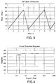
- FIGS. 1-4 show typical data collected for the 180 degree phase modulation.
- FIG. 2 shows the Fourier transform of the 180 degree phase modulation data of FIG. 1.
- FIG. 3 shows typical data collected for the 90 degree phase modulation, and
- FIG. 4 the Fourier transform of this collected data.
- FIGS. 1-4 confirms that a pulse-to-pulse phase increment of (360 degrees/N) yields a line in the Fourier transform spectrum at (PRF/N). The converse also holds true, so that a line at (PRF/N) implies a phase increment of (360 degrees/N). This allows for a check of the functionality of the module's phase shifter.
- the absolute phase difference is the phase transmit (phase state 0) minus the phase receive -(phase state 0), equal to where s is the collected signal, phase state 0 is an arbitrary reference phase state, and FS(PRF/N) is the (PRF/N) filter of the Fourier transform of the signals.
- the relative phase difference between the transmit module and the receive module under test is the arc tangent of the resultant line in the FFT of the collected data.
- the offset data resulting from the calibration can be used to provide corrections to the control signals applied by the beam forming computer 90 to steer the beam.
- Exemplary techniques for the application of this offset data to develop the corrections to the phase shifter commands are described in applicants' commonly assigned, co-pending European patent application serial number , filed , claiming priority of U.S. patent application S.N. 642,033 of May 2, 1996 "Self-Phase Up of Array Antennas With Non-Uniform Element Mutual Coupling and Arbitrary Lattice Orientations", (Attorney's Docket 2405P678EP), the entire contents of which being incorporated herein by this reference.
- the procedure begins by commanding the whole array to the safe state.
- a module next to the module under test is switched to the transmit state by using the T/R toggle command.
- the module under test is then amplitude modulated using the amplitude modulation mode command to decrement the amplitude from pulse to pulse.
- Data is collected and processed, and the derived amplitude offsets and states are stored in the calibration tables.
- the process uses successive refining to test each of the bits in the test module's attenuation control.
- the first test is to ramp the attenuation 1.0, 0.5, 1.0, 0.5, and so on.
- the next test is to ramp the attenuation 1.00, 0.75, 0.50, 0.25, 1.00, 0.75, and so on.
- the process is repeated in the finest level on control of the module.
- the ratio of amplitude transmit (state 0) and amplitude receive (state 0) is equal to where s is the modulated, time-domain, receive signal, state 0 is an arbitrary reference amplitude, (PRF/2) denotes the line at (PRF/2) in the Fourier Transform spectrum, ( ⁇ A) is the attenuation increment (0.5, 0.25, etc.), (N FFT ) is the number of points in the FFT.
- the receive amplitude and phase calibration procedures can both be completed for a given module before calibrating another module, as illustrated in the exemplary flow diagram of FIG. 11.
- the T/R module of interest is commanded to the receive mode, and to the modulated state (step 212).
- the various phase and gain measurements are performed, wherein the gain and phase control assembly 118 is steps through the various gain and phase steps as described above.
- the offset terms are calculated from the measurement data, using equations 1 and 2.
- the offset terms are stored and applied.
- operation loops to the next module for its calibration.
- the transmit phase procedure is identical to the receive phase procedure with the following modifications:
- the transmit amplitude procedure is identical to the receive amplitude procedure with the following modifications;
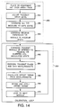
- FIG. 14 shows the general transmit calibration procedure, wherein both the phase and amplitude calibrations are performed for a module.
- the transmit phase and gain measurements are performed to collect the measurement data.
- the offset terms are calculated from the measurement data.
- the offset terms are stored and applied.
- Step 270 shows the process flow looping to the next module to be calibrated.
- the transmit portion of the calibration process works within certain limitations.
- the procedures here would provide tests for phase and amplitude control functionality, module-to-module phase and gain offsets, and measurements of the associated feed-structure phase and amplitudes.
- a "clump” is defined as a group of elements in proximity to a central reference element.
- FIGS. 9A and 9B illustrate a triangular lattice.
- a clump 20 in FIG. 9A includes a center reference element 22 surrounded by elements 20A-20F. The previous procedures collect the phase and amplitude offsets from the central element 22. These offsets are then used to command the surrounding modules connected to elements 20A-20F to the same phase and amplitude (within ⁇ ) as the central element 22.
- FIG. 9B depicts a clump of clumps, wherein clumps 20, 26, 28, 32, 34, 36 surround a center clump 30.
- Adjacent clumps are then calibrated with respect to a central clump by comparing offsets from adjacent bordering elements. The process is repeated recursively until the array is calibrated. Using this technique, the maximum error across the array should be on the order of log 2 (nx*ny)* ⁇ , where z equals the number of elements within a clump.
- FIG. 10A is similar to FIG. 9A, but shows a rectangular lattice arrangement, wherein a clump 34 is defined by a center element 36 surrounded by elements 34A-34H.
- FIG. 10B shows a clump of clumps of elements in the rectangular lattice.
- T/R Module Requirements The following requirements are placed on the system for self-calibration; T/R Module Requirements:
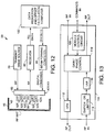
- FIGS. 12 and 13 illustrate in block diagram a system 50 meeting these requirements.
- the system includes an array 60, which comprises a plurality of radiating elements 62A-62F, each of which is connected to a corresponding T/R module.
- FIG. 13 shows an exemplary one of the T/R modules 110.
- a transmit drive source 70 is connected to the array to drive the radiating elements, typically through a feed network comprising the array.
- a receiver 80 is responsive to signals received at the radiating elements and collected through the T/R modules and a receive feed.
- the receiver provides complex I/R receive data to a data reduction and offset calculation computer 100.
- a beam forming computer 90 provides digital commands to the T/R modules to set the array to form a desired beam steered in a given direction.
- the beam forming computer applies offset data calculated by the computer 100 as a result of the array self-calibration, in order to accurately form the beam.
- the T/R modules are represented by exemplary module 110 in FIG. 13.
- the RF signal from the transmit source is passed through a gain and phase control assembly 118, which includes independently controllable gain/attenuator stages and phase shifters, which are adjusted during the calibration mode as described above.
- the digital commands from the computer 90 are sent to the module control circuit (MCC) 120, which in turn controls the gain and phase shifter settings of assembly 118.
- MCC module control circuit
- the output from the gain setting stages of assembly 118 is then passed through the high power amplifier (HPA) 112 which amplifies the transmit signal and passes the amplified signal on to the corresponding radiating element.
- HPA high power amplifier
- the signal from the radiating element is passed through a switch or limiter 114, then through a low noise amplifier (LNA) 116, and the amplified signal on receive is passed through the gain and phase control assembly 118 to be appropriately attenuated/amplified and phase shifted according to the instructions from the beam forming computer 90.
- the received RF output signal is then passed to the receiver 80.
- LNA low noise amplifier
- one module will be commanded to the transmit mode, say element 62D, an adjacent module will be commanded to the receive mode, say the module for element 62C, and the remaining modules for elements 62A, 62B, 62E and 62F will be commanded to the safe state.
Landscapes
- Radar Systems Or Details Thereof (AREA)
- Variable-Direction Aerials And Aerial Arrays (AREA)
- Arrangements For Transmission Of Measured Signals (AREA)
Abstract
Description
- This invention relates to techniques for calibration of phased array antenna systems, and more particularly to a technique for collecting phase and/or amplitude calibration data for a phased array system without the use of external sensors.
- One known approach to array calibration is a two step process. First, phase and amplitude calibration information is collected at a subarray level. Then the subarrays are assembled, the feeds are attached, and the array is re-calibrated as a whole unit. The re-calibration process requires the use of a high-power nearfield scanner and its associated hardware.
- This known approach to array calibration has several disadvantages. The high-power nearfield scanner is a very expensive asset. The calibration/phase-up process takes many test hours with this asset. The high-power nature of the scanner requires special safety considerations. The calibration process can only be performed in the laboratory with the use of the high-power scanner. No field calibration of the transmit/receive (T/R) modules of the system is possible. Field testing of the T/R module functionality requires the use of an external sensor. Finally, distributed-monopulse-hybrid calibration requires the injection of an identical signal into each of the monopulse hybrids.
- One aspect of the invention is a technique for collecting phase and amplitude calibration data for an active array system without the use of external sensors, such as a planar nearfield. The relative phase and amplitudes of T/R modules are determined when viewed through the entire array system. The calibration process involves collecting and storing these phases and amplitudes for future use. A pulse-to-pulse phase or amplitude modulation mode is employed An element is commanded into this mode to separate its signal (in frequency) from competing signals and leakages from the surrounding modules. A single element is switched to a transmit state while the remainder of the array is in the receive state. This provides for a reference signal during receive calibration, and for single module testing during transmit calibration.
- Thus, in accordance with the invention, a method for receive self calibration of an active RF antenna array system is described, comprising the following steps:
- (a) placing a radar absorbing hat over the array aperture;
- (b) setting the transmit drive to an appropriate level to obtain linear operation of the receive module;
- (c) setting a given T/R module under test to a receive state;
- (d) setting a reference T/R module to a transmit state;
- (e) setting all other T/R modules in the array except the module under test and the reference module to a safe state so as not to transmit or receive through said other modules;
- (f) receiving pulses of RF energy at the module under test via its corresponding radiating element which has been transmitted through the reference module via its corresponding radiating element;
- (g) changing the state of the phase shifting circuitry of the receive module under test on a pulse-to-pulse or between groups of pulses to add phase modulation to the received pulses of energy to collect measurement data;
- (h) analyzing the measurement data to determine the relative phase difference between the transmit module and the receive module under test;
- (i) repeating the calibration for other modules in the array to obtain a set of data indicating the relative phase differences between the modules in the array, wherein only one module is transmitting and only one module is receiving during a test of a module under test; and
- (j) storing the set of data for use in setting the phase shifters for accurate receive beam forming.
- A receive amplitude calibration method is further described, wherein amplitude modulation is applied on the signal by the module under test, by incrementing the module's gain control circuitry to decrease the amplitude from pulse to pulse. A Fourier transform is performed on the measured data, and the transformed spectrum is analyzed to provide a check on functionality of the gain control circuitry and to measure the relative amplitudes between the reference module and the module under test.
- Similar transmit phase and amplitude calibration methods are described, which are similar to the receive calibration methods except that the module under test is set to transmit, and the reference module is set to receive.
- These and other features and advantages of the present invention will become more apparent from the following detailed description of an exemplary embodiment thereof, as illustrated in the accompanying drawings, in which:
- FIG. 1 shows typical data collected for a 180 degree phase modulation in the receive phase procedure in accordance with the invention.
- FIG. 2 shows the Fourier transform of the 180 degree phase modulation data of FIG. 1.
- FIG. 3 shows typical data collected for a 90 degree phase modulation in the receive phase procedure in accordance with the invention.
- FIG. 4 shows the Fourier transform of the collected data of FIG. 3.
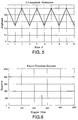
- FIG. 5 shows typical amplitude modulation collected £or the 0.5 attenuation level in the receive amplitude procedure in accordance with the invention.
- FIG. 6 shows the Fourier transform of the 0,5 amplitude modulation data of FIG. 5.
- FIG. 7 shows typical amplitude modulation collected for the 0.25 attenuation level in the receive amplitude procedure in accordance with the invention.
- FIG. 8 shows the Fourier transform of the 0.25 amplitude modulation data of FIG. 7.
- FIGS. 9 and 10 show a "clumping" technique to minimize propagation of error effects for rhombic and rectangular lattices, respectively.
- FIG. 11 is a flow diagram illustrating an exemplary receive calibration technique in accordance with the invention.
- FIG. 12 is a system block diagram of an array system embodying the invention.
- FIG. 13 is a block diagram of a transmit/receive module embodying the invention.
- FIG. 14 is a flow diagram illustrating an exemplary transmit calibration technique in accordance with the invention.
- The purpose of this invention is to provide a way of collecting active array calibration data without the use of an external sensor system, such as a planar nearfield. The technique provides a way of performing array self-calibration, and requires only the use of an external radar-absorbing hat. The array self-calibration process is broken dawn into the following components: 1) receive calibration, receive phase calibration and receive amplitude calibration procedures, 2) transmit calibration procedure, transmit phase calibration procedure, transmit amplitude calibration procedure, and transmit calibration limitations, 3) propagation of error effects (clumping), 4) system requirements, and 5) test requirements. These components will be discussed in turn.
- The following module commands and test setups are used for all receive calibration tests. The system setup procedures (200) are illustrated in the flow diagram of FIG. 11.
- 1. An RF-absorbent hat 40 (FIG. 12) is placed over the array to limit element-to-element signals to those due solely to mutual coupling (step 202). The hat is typically a fitted box which slides over the array. The inside of the hat is lined with RF-
absorbent material 42. - 2. The system may require a reduced transmit drive level dependent on module receive characteristics (step 204). The level of this drive shall be such that the coupled power from the transmit module at the input to the receive module shall be equal to the maximum allowable for linear operation of the receive module.
- 3. For the transmit/receive (T/R) modules not under test, the high power amplifiers (HPAs) 112 (FIG. 13) are enabled to approximately the array thermal environment during normal operation. The modules are otherwise disabled, so as not to transmit or receive, in a "safe" state (step 206).
- 4. For the transmit reference module, the
HPA 112 is enabled, the T/R bit is set to inverted so that it transmits while other modules receive (step 210). - 5. For the receive module under test, the low noise amplifier (LNA) 116 (FIG. 13) is enabled, the T/R bit is set to normal, and the module is commanded into a mode using pulse-to-pulse phase or amplitude modulation to separate its signal in frequency from competing signals and leakages from the surrounding modules (step 212).
- The procedure begins by commanding the whole array to a receive state. A reference module is switched to the transmit state by using the T/R inversion command built into the module's control circuitry. The module under test is then phase-modulated using a special command to increment the phase from pulse to pulse. Data is collected and processed as described in Eq. 1 and Eq. 2, and the derived phase offsets and states are stored in beamforming tables inside the beam forming computer 90 (FIG. 12).
- The process uses successive refining to test each of the bits in the test module's phase shifter. The first test is to rotate the
phase 0 degrees, 180 degrees, 0 degrees (360 degrees), 180 degrees (540 degrees), and so on, The next test is to rotate thephase 0 degrees, 90 degrees, 180 degrees, 270 degrees, 0 degrees (360 degrees), 90 degrees (450 degrees) and so on. The process is repeated to the finest level on phase control of the module. - Using the modulation just described, data is collected, and a Fourier transform is performed on the collected data, as illustrated in FIGS. 1-4. FIG, 1 shows typical data collected for the 180 degree phase modulation. FIG. 2 shows the Fourier transform of the 180 degree phase modulation data of FIG. 1. Similarly, FIG. 3 shows typical data collected for the 90 degree phase modulation, and FIG. 4 the Fourier transform of this collected data.
- Examination of FIGS. 1-4 confirms that a pulse-to-pulse phase increment of (360 degrees/N) yields a line in the Fourier transform spectrum at (PRF/N). The converse also holds true, so that a line at (PRF/N) implies a phase increment of (360 degrees/N). This allows for a check of the functionality of the module's phase shifter.
- To arrive at the absolute phase difference between the transmit module and the receive module under test, the following formula is used. The absolute phase difference is the phasetransmit(phase state 0) minus the phasereceive-(phase state 0), equal to

phase state 0 is an arbitrary reference phase state, and FS(PRF/N) is the
(PRF/N) filter of the Fourier transform of the signals. In simplified terms, the relative phase difference between the transmit module and the receive module under test is the arc tangent of the resultant line in the FFT of the collected data. - The offset data resulting from the calibration can be used to provide corrections to the control signals applied by the
beam forming computer 90 to steer the beam. Exemplary techniques for the application of this offset data to develop the corrections to the phase shifter commands are described in applicants' commonly assigned, co-pending European patent application serial number , filed , claiming priority of U.S. patent application S.N. 642,033 of May 2, 1996 "Self-Phase Up of Array Antennas With Non-Uniform Element Mutual Coupling and Arbitrary Lattice Orientations", (Attorney's Docket 2405P678EP), the entire contents of which being incorporated herein by this reference. - The procedure begins by commanding the whole array to the safe state. A module next to the module under test is switched to the transmit state by using the T/R toggle command. The module under test is then amplitude modulated using the amplitude modulation mode command to decrement the amplitude from pulse to pulse. Data is collected and processed, and the derived amplitude offsets and states are stored in the calibration tables.
- The process uses successive refining to test each of the bits in the test module's attenuation control. The first test is to ramp the attenuation 1.0, 0.5, 1.0, 0.5, and so on. The next test is to ramp the attenuation 1.00, 0.75, 0.50, 0.25, 1.00, 0.75, and so on. The process is repeated in the finest level on control of the module.
- Using the previously described modulation, data is collected and a Fourier transform is performed on the collected data. Typical collected data and corresponding transform outputs are illustrated in FIGS, 5-8.
- For a pulse-to-pulse attenuation increment of (l/N), N lines can be seen, starting at 0 and spaced every (PRF/N). The converse also holds true, so if there are N lines at (PRF/N), it can be seen that the corresponding attenuation increment was (l/N).
- To derive the ratio of the amplitude differences between the two modules (the one in transmit and the other in receive), the following formula is used. The ratio of amplitudetransmit(state 0) and amplitudereceive(state 0) is equal to

state 0 is an arbitrary reference amplitude, (PRF/2) denotes the line at (PRF/2) in the Fourier Transform spectrum, (ΔA) is the attenuation increment (0.5, 0.25, etc.), (NFFT) is the number of points in the FFT. - In an exemplary implementation, the receive amplitude and phase calibration procedures can both be completed for a given module before calibrating another module, as illustrated in the exemplary flow diagram of FIG. 11. As shown therein, the T/R module of interest is commanded to the receive mode, and to the modulated state (step 212). At
step 214, the various phase and gain measurements are performed, wherein the gain andphase control assembly 118 is steps through the various gain and phase steps as described above. Atstep 216, the offset terms are calculated from the measurement data, usingequations step 218, the offset terms are stored and applied. Atstep 220, operation loops to the next module for its calibration. - The following procedure commands and test setups are used for all transmit calibration tests, as illustrated in the system setup procedure 250 (FIG. 14).
- 1. The radar absorbent hat (40) is placed over the array (60) to limit element-to-element signals to those due solely to mutual coupling (step 252).
- 2. The system may require a reduced transmit drive level dependent on module receive characteristics. The level of this drive shall be such that the coupled power from the transmit module at the input of the receive module shall be equal to the maximum allowable for linear operation of the receive module (step 254).
- 3. For the T/R modules not under test, the HPAs are enabled to approximate the operational array thermal environment during normal operation. The modules are otherwise disabled (LNA and gain/phase control circuitry disabled), so as not to transmit or receive (step 256).
- 4. In the calibration loop, for the receive reference module, the LNA (116) is enabled, and the T/R bit is set to normal.
- 5. In the calibration loop 260 (FIG. 14), for the transmit module under test, the HPA (112) is enabled, the T/R bit is set to inverted (T/R toggled to transmit), and the module is commanded into a mode using pulse-to-pulse phase or amplitude modulation to separate its signal in frequency from competing signals and leakages from the surrounding modules (step 262).
- The transmit phase procedure is identical to the receive phase procedure with the following modifications:
- 1. The reference module is operated in a receive state.
- 2. The module under test is transmitting.
- The transmit amplitude procedure is identical to the receive amplitude procedure with the following modifications;
- 1. The reference module is operated in a receive state.
- 2. The module under test is transmitting.
- FIG. 14 shows the general transmit calibration procedure, wherein both the phase and amplitude calibrations are performed for a module. At
step 264, the transmit phase and gain measurements are performed to collect the measurement data. Atstep 266, the offset terms are calculated from the measurement data. Atstep 268, the offset terms are stored and applied. Step 270 shows the process flow looping to the next module to be calibrated. - The transmit portion of the calibration process works within certain limitations. The procedures here would provide tests for phase and amplitude control functionality, module-to-module phase and gain offsets, and measurements of the associated feed-structure phase and amplitudes.
- Assuming that an accurate measurement can be made from module to module, there still is the issue of the residual error in this measurement. It an error of size Δ is created from module to module, a maximum error of (nx+ny)Δ would be created across the array face due to the cascading of the independent measurements. The cumulative effects of this excess error could be prohibitive.
- A "clump" is defined as a group of elements in proximity to a central reference element. FIGS. 9A and 9B illustrate a triangular lattice. A
clump 20 in FIG. 9A includes acenter reference element 22 surrounded byelements 20A-20F. The previous procedures collect the phase and amplitude offsets from thecentral element 22. These offsets are then used to command the surrounding modules connected toelements 20A-20F to the same phase and amplitude (within Δ) as thecentral element 22. FIG. 9B depicts a clump of clumps, wherein clumps 20, 26, 28, 32, 34, 36 surround acenter clump 30. Adjacent clumps are then calibrated with respect to a central clump by comparing offsets from adjacent bordering elements. The process is repeated recursively until the array is calibrated. Using this technique, the maximum error across the array should be on the order of log2(nx*ny)*Δ, where z equals the number of elements within a clump. - FIG. 10A is similar to FIG. 9A, but shows a rectangular lattice arrangement, wherein a
clump 34 is defined by acenter element 36 surrounded byelements 34A-34H. FIG. 10B shows a clump of clumps of elements in the rectangular lattice. - The following requirements are placed on the system for self-calibration;
T/R Module Requirements: - 1. Modules must support logic inversion of the transmit/receive command.
- 2. Modules or beam forming computer must support pulse-to-pulse and amplitude modulation functions for all control bits.
- 3. Modules must have selective enable capability. That is, HPAs and LNAs can be enabled and disabled through logic commands.
- 4. Modules (active array elements) must be capable of linear receive operation with the power levels used for this testing.
- 5. The array system must support single-element receive measurement while transmit drive excitation is applied.
- FIGS. 12 and 13 illustrate in block diagram a
system 50 meeting these requirements. The system includes anarray 60, which comprises a plurality of radiating elements 62A-62F, each of which is connected to a corresponding T/R module. FIG. 13 shows an exemplary one of the T/R modules 110. A transmitdrive source 70 is connected to the array to drive the radiating elements, typically through a feed network comprising the array. Areceiver 80 is responsive to signals received at the radiating elements and collected through the T/R modules and a receive feed. The receiver provides complex I/R receive data to a data reduction and offsetcalculation computer 100. Abeam forming computer 90 provides digital commands to the T/R modules to set the array to form a desired beam steered in a given direction. The beam forming computer applies offset data calculated by thecomputer 100 as a result of the array self-calibration, in order to accurately form the beam. - The T/R modules are represented by
exemplary module 110 in FIG. 13. The RF signal from the transmit source is passed through a gain andphase control assembly 118, which includes independently controllable gain/attenuator stages and phase shifters, which are adjusted during the calibration mode as described above. The digital commands from thecomputer 90 are sent to the module control circuit (MCC) 120, which in turn controls the gain and phase shifter settings ofassembly 118. The output from the gain setting stages ofassembly 118 is then passed through the high power amplifier (HPA) 112 which amplifies the transmit signal and passes the amplified signal on to the corresponding radiating element. On receive, the signal from the radiating element is passed through a switch orlimiter 114, then through a low noise amplifier (LNA) 116, and the amplified signal on receive is passed through the gain andphase control assembly 118 to be appropriately attenuated/amplified and phase shifted according to the instructions from thebeam forming computer 90. The received RF output signal is then passed to thereceiver 80. - In an exemplary calibration, one module will be commanded to the transmit mode, say element 62D, an adjacent module will be commanded to the receive mode, say the module for element 62C, and the remaining modules for elements 62A, 62B, 62E and 62F will be commanded to the safe state.
- The following requirements are placed on the test for array self-calibration:
- 1. The array self-calibration is greatly simplified if there is only one path for energy to travel from one T/R module to another. The path of energy transfer which unavoidable is that of mutual coupling. Mutual coupling is defined as the dominant signal source, and a radar-
absorbent hat 40 is placed over the array to eliminate possible unwanted reflected returns. A simple formula exist for the required absorbency of this hat:
- 2. Interference signals and leakage signals from the modules not involved in the test have no modulation placed on them. This causes them to separate from the desired measurement signal on the output of the Fourier transform. If these signals are of sufficient strength, the Fourier transform filter sidelobes of this return may interfere with the measurements of the one of the modulation lines. The solution to this problem is to limit the size of the interference signals where practical, and to collect larger data sets for FFT processing, thus giving finer filters.
- It is understood that the above-described embodiments are merely illustrative of the possible specific embodiments which may represent principles of the present invention. Other arrangements may readily be devised in accordance with these principles by those skilled in the art without departing from the scope and spirit of the invention.
Claims (9)
- A method for receive self calibration of an active RF antenna array system (60) comprising a plurality of radiating elements (62A-62F) arranged in an array aperture, a corresponding plurality of transmit/receive modules (110) each including independently adjustable phase shifting circuitry (118), a transmit signal source for providing transmit signals and a receiver responsive to the signals received through the radiating elements (62A-62F), and T/R modules (110) to provide a receiver signal, the method comprising the following steps:(a) placing a radar absorbing hat (40) over the array aperture;(b) setting a transmit drive (70) to an appropriate level to obtain linear operation of the receive module (110);(c) setting a given T/R module (110) under test to a receive state;(d) setting a reference T/R module (110) to a transmit state;(e) setting all other T/R modules (110) in the array (60) except the module (110) under test and the reference module (110) to a safe state so as not to transmit or receive through other modules (110);(f) receiving pulses of RF energy at the module (110) under test via its corresponding radiating element (62A-62F) which has been transmitted through the reference module (110) via its corresponding radiating element (62A-62F);(g) changing the state of the phase shifting circuitry (118) of the receive module (110) under test on a pulse-to-pulse or between groups of pulses to add phase modulation to the received pulses of energy to collect measurement data;(h) analyzing the measurement data to determine the relative phase difference between the transmit module (110) and the receive module (110) under test;(i) repeating the calibration for other modules (110) in the array (60) to obtain a set of data indicating the relative phase differences between the modules (110) in the array (60), wherein only one module (110) is transmitting and only one module (110) is receiving during a test of a module (110) under test; and(j) storing the set of data for use in setting the phase shifters (118) for accurate receive beam forming.
- A method for transmit self calibration of an active RF antenna array system (60) comprising a plurality of radiating elements (62A-62F) arranged in an array aperture, a corresponding plurality of transmit/receive modules (110) each including independently adjustable phase shifting circuitry (118), a transmit signal source for providing transmit signals and a receiver responsive to the signals received through the radiating elements (62A-62F), and T/R modules (110) to provide a receiver signal, the method comprising the following steps:(a) placing a radar absorbing hat (40) over the array aperture;(b) setting a transmit drive (70) to an appropriate level to obtain linear operation of the receive module (110);(c) setting a given T/R module (110) under test to a transmit state;(d) setting a reference T/R module (110) to a receive state;(e) setting all other T/R modules (110) in the array (60) except the module (110) under test and the reference module (110) to a safe state so as not to transmit or receive through other modules (110);(f) receiving pulses of RF energy at the module (110) under test via its corresponding radiating element (62A-62F) which has been transmitted through the module (110) under test via its corresponding radiating element (62A-62F);(g) changing the state of the phase shifting circuitry (118) of the module (110) under test on a pulse-to-pulse or between groups of pulses to add phase modulation to the received pulses of energy to collect measurement data;(h) analyzing the measurement data to determine the relative phase difference between the module (110) under test and the receive module (110);(i) repeating the calibration for other modules (110) in the array (60) to obtain a set of data indicating the relative phase differences between the modules (110) in the array (60), wherein only one module (110) is transmitting and only one module (110) is receiving during a test of a module (110) under test; and(j) storing the set of data for use in setting the phase shifters (118) for accurate receive beam forming.
- The method of claim 1 or 2, characterized in that the step of changing the state of the phase shifting circuitry (118) comprises incrementing the phase shift applied by the phase shifting circuitry (118) between pulses, and the step of analyzing the measurement data comprises performing a Fourier transform on the collected data.
- The method of any of claims 1 - 3, characterized in that the step of analyzing the measurement data further comprises analyzing the Fourier transform spectrum for lines at expected values corresponding to the phase shift increment.
- The method of any of claims 1 - 4, characterized in that the T/R modules (110) include a high power amplifier (112) for transmit operation, and those T/R modules (110) set to the safe state have their high power amplifiers (112) enabled to the extent necessary to approximate the array thermal environment during normal operation.
- The method of any of claims 1 - 5, characterized in that each T/R module (110) further includes independently controllable gain control circuitry (118) to vary the power of signals passed through the module (110), and wherein the method further includes a method for amplitude calibration of the T/R modules (110), comprising the following steps:(a) for the module (110) under test, changing the gain control circuitry (118) of the module (110) under test from pulse-to-pulse or between groups of pulses to apply amplitude modulation to the received signal;(b) analyzing the measurement data to determine the relative amplitude difference between the transmit module (110) or the module (110) under test, respectively, and the receive module (110) or the reference module (110), respectively;(c) repeating the calibration for other modules (110) in the array (60) to obtain a set of data indicating the relative amplitude differences between the modules (110) in the array (60), wherein only one module (110) is transmitting and only one module (110) is receiving during a test of a module (110) under test; and(d) storing the set of data for use in setting the gain control circuitry (118) during normal operation;
- The method of claim 6, characterized in that the step of changing the gain control circuitry (118) includes decrementing the amplitude from pulse to pulse, and the step of analyzing the measurement data comprises performing a Fourier transform on the measurement data.
- An apparatus for receive self calibration of an active RF antenna array system (60) comprising a plurality of radiating elements (62A-62F) arranged in an array aperture, a corresponding plurality of transmit/receive modules (110) each including independently adjustable phase shifting circuitry (118), a transmit signal source for providing transmit signals and a receiver responsive to the signals received through the radiating elements (62A-62F), and T/R modules (110) to provide a receiver signal, the apparatus comprising:(a) means for placing a radar absorbing hat (40) over the array aperture;(b) means for setting a transmit drive (70) to an appropriate level to obtain linear operation of the receive module (110);(c) means for setting a given T/R module (110) under test to a receive state;(d) means for setting a reference T/R module (110) to a transmit state;(e) means for setting all other T/R modules (110) in the array (60) except the module (110) under test and the reference module (110) to a safe state so as not to transmit or receive through other modules (110);(f) means for receiving pulses of RF energy at the module (110) under test via its corresponding radiating element (62A-62F) which has been transmitted through the reference module (110) via its corresponding radiating element (62A-62F);(g) means for changing the state of the phase shifting circuitry (118) of the receive module (110) under test on a pulse-to-pulse or between groups of pulses to add phase modulation to the received pulses of energy to collect measurement data;(h) means for analyzing the measurement data to determine the relative phase difference between the transmit module (110) and the receive module (110) under test;(i) means for repeating the calibration for other modules (110) in the array (60) to obtain a set of data indicating the relative phase differences between the modules (110) in the array (60), wherein only one module (110) is transmitting and only one module (110) is receiving during a test of a module (110) under test; and(j) means for storing the set of data for use in setting the phase shifters (118) for accurate receive beam forming.
- An apparatus for transmit self calibration of an active RF antenna array system (60) comprising a plurality of radiating elements (62A-62F) arranged in an array aperture, a corresponding plurality of transmit/receive modules (110) each including independently adjustable phase shifting circuitry (118), a transmit signal source for providing transmit signals and a receiver responsive to the signals received through the radiating elements (62A-62F), and T/R modules (110) to provide a receiver signal, the apparatus comprising the following steps:(a) means for placing a radar absorbing hat (40) over the array aperture;(b) means for setting a transmit drive (70) to an appropriate level to obtain linear operation of the receive module (110);(c) means for setting a given T/R module (110) under test to a transmit state;(d) means for setting a reference T/R module (110) to a receive state;(e) means for setting all other T/R modules (110) in the array (60) except the module (110) under test and the reference module (110) to a safe state so as not to transmit or receive through other modules (110);(f) means for receiving pulses of RF energy at the module (110) under test via its corresponding radiating element (62A-62F) which has been transmitted through the module (110) under test via its corresponding radiating element (62A-62F);(g) means for changing the state of the phase shifting circuitry (118) of the module (110) under test on a pulse-to-pulse or between groups of pulses to add phase modulation to the received pulses of energy to collect measurement data;(h) means for analyzing the measurement data to determine the relative phase difference between the module (110) under test and the receive module (110);(i) means for repeating the calibration for other modules (110) in the array (60) to obtain a set of data indicating the relative phase differences between the modules (110) in the array (60), wherein only one module (110) is transmitting and only one module (110) is receiving during a test of a module (110) under test; and(j) means for storing the set of data for use in setting the phase shifters (118) for accurate receive beam forming.
Applications Claiming Priority (2)
| Application Number | Priority Date | Filing Date | Title |
|---|---|---|---|
| US643132 | 1996-05-02 | ||
| US08/643,132 US5682165A (en) | 1996-05-02 | 1996-05-02 | Active array self calibration |
Publications (3)
| Publication Number | Publication Date |
|---|---|
| EP0805510A2 true EP0805510A2 (en) | 1997-11-05 |
| EP0805510A3 EP0805510A3 (en) | 2000-03-29 |
| EP0805510B1 EP0805510B1 (en) | 2003-03-12 |
Family
ID=24579483
Family Applications (1)
| Application Number | Title | Priority Date | Filing Date |
|---|---|---|---|
| EP97107197A Expired - Lifetime EP0805510B1 (en) | 1996-05-02 | 1997-04-30 | Active array self calibration |
Country Status (6)
| Country | Link |
|---|---|
| US (1) | US5682165A (en) |
| EP (1) | EP0805510B1 (en) |
| JP (1) | JP3331143B2 (en) |
| AU (1) | AU690870B2 (en) |
| CA (1) | CA2203964C (en) |
| DE (1) | DE69719592T2 (en) |
Cited By (8)
| Publication number | Priority date | Publication date | Assignee | Title |
|---|---|---|---|---|
| EP0954053A3 (en) * | 1998-04-28 | 2000-10-25 | Matsushita Electric Industrial Co., Ltd. | Array antenna radio communication apparatus |
| EP1178562A1 (en) * | 2000-08-03 | 2002-02-06 | Telefonaktiebolaget L M Ericsson (Publ) | Antenna array calibration |
| EP1394563A1 (en) * | 2002-08-21 | 2004-03-03 | Robert Bosch Gmbh | Online calibration of a phased array antenna for radar |
| EP1670095A1 (en) * | 2004-12-07 | 2006-06-14 | Lockheed Martin Corporation | Mutual coupling method for calibrating a phased array |
| EP1585231A4 (en) * | 2002-12-25 | 2006-12-06 | Da Tang Mobile Comm Equipment | A method for calibrating smart antenna array systems in real time |
| EP3203267A1 (en) | 2016-02-05 | 2017-08-09 | Thales | Method for calibrating a satellite radionavigation receiver |
| KR20200080034A (en) * | 2018-12-26 | 2020-07-06 | 삼성전자주식회사 | A method for testing a wireless communication module, and an electronic device including the wireless communication module |
| US11824272B2 (en) | 2016-10-26 | 2023-11-21 | International Business Machines Corporation | In-field millimeter-wave phased array radiation pattern estimation and validation |
Families Citing this family (41)
| Publication number | Priority date | Publication date | Assignee | Title |
|---|---|---|---|---|
| JP4557429B2 (en) * | 1998-11-24 | 2010-10-06 | インテル・コーポレーション | Method and apparatus for calibrating a wireless communication station having an array antenna |
| SE515141C2 (en) * | 2000-03-22 | 2001-06-18 | Ericsson Telefon Ab L M | Self-calibration of feed lines for group antennas |
| DE10259863A1 (en) * | 2002-12-20 | 2004-07-08 | Robert Bosch Gmbh | Angle scanning radar system |
| JP4195670B2 (en) * | 2004-02-27 | 2008-12-10 | 三菱重工業株式会社 | Transmission wave phase control method and apparatus |
| JP2006003097A (en) * | 2004-06-15 | 2006-01-05 | Fujitsu Ten Ltd | Radar device |
| US7081851B1 (en) | 2005-02-10 | 2006-07-25 | Raytheon Company | Overlapping subarray architecture |
| US7161530B2 (en) * | 2005-02-22 | 2007-01-09 | The United States Of America As Represented By The Secretary Of The Army | System and method for radar calibration using antenna leakage |
| US7471237B2 (en) * | 2006-03-22 | 2008-12-30 | The Boeing Company | Built-in missile RADAR calibration verification |
| US7522096B2 (en) * | 2007-04-09 | 2009-04-21 | Honeywell International Inc | Method for phase calibrating antennas in a radar system |
| EP2234539B1 (en) * | 2007-12-28 | 2015-05-20 | Interstitial, LLC | Synthetic aperture radar system |
| US20100321233A1 (en) * | 2009-06-18 | 2010-12-23 | Alvarion Ltd. | Method for calibrating antenna arrays |
| US8184042B2 (en) * | 2009-07-02 | 2012-05-22 | The Boeing Company | Self calibrating conformal phased array |
| US8154452B2 (en) * | 2009-07-08 | 2012-04-10 | Raytheon Company | Method and apparatus for phased array antenna field recalibration |
| US8842040B1 (en) * | 2010-06-17 | 2014-09-23 | The United States Of America, As Represented By The Secretary Of The Navy | Mutual coupling based calibration technique for structurally deformed phased array apertures |
| US20110319034A1 (en) | 2010-06-28 | 2011-12-29 | Boe Eric N | Method and system for propagation time measurement and calibration using mutual coupling in a radio frequency transmit/receive system |
| US8280312B2 (en) | 2010-07-22 | 2012-10-02 | Raytheon Company | Method and system for signal distortion characterization and predistortion compensation using mutual coupling in a radio frequency transmit/receive system |
| DK2458400T3 (en) * | 2010-11-27 | 2013-10-14 | Eads Deutschland Gmbh | Method of directional reflection using monopulse formation |
| US9124361B2 (en) * | 2011-10-06 | 2015-09-01 | Raytheon Company | Scalable, analog monopulse network |
| US8692707B2 (en) * | 2011-10-06 | 2014-04-08 | Toyota Motor Engineering & Manufacturing North America, Inc. | Calibration method for automotive radar using phased array |
| US9170320B1 (en) * | 2012-12-03 | 2015-10-27 | Lockheed Martin Corporation | Transmitter pushing compensation for radar stability enhancement |
| US9702928B2 (en) | 2014-01-15 | 2017-07-11 | The Boeing Company | Self-healing array system and method |
| US9453906B2 (en) * | 2014-07-31 | 2016-09-27 | North Carolina State University | Phase calibration circuit and method for multi-channel radar receiver |
| US10371798B2 (en) * | 2015-12-01 | 2019-08-06 | Raytheon Company | Array and module calibration with delay line |
| US10200075B2 (en) * | 2016-03-04 | 2019-02-05 | Raytheon Company | Discrete time analog signal processing for simultaneous transmit and receive |
| CN106209269B (en) * | 2016-07-27 | 2018-09-28 | 华东师范大学 | The calibration method of spherical surface composite array near-field effect in a kind of radio freqency simulation system |
| US20180062260A1 (en) * | 2016-08-26 | 2018-03-01 | Analog Devices Global | Antenna array calibration systems and methods |
| US10751126B2 (en) | 2016-10-28 | 2020-08-25 | Covidien Lp | System and method for generating a map for electromagnetic navigation |
| US10638952B2 (en) | 2016-10-28 | 2020-05-05 | Covidien Lp | Methods, systems, and computer-readable media for calibrating an electromagnetic navigation system |
| US10517505B2 (en) | 2016-10-28 | 2019-12-31 | Covidien Lp | Systems, methods, and computer-readable media for optimizing an electromagnetic navigation system |
| US10792106B2 (en) | 2016-10-28 | 2020-10-06 | Covidien Lp | System for calibrating an electromagnetic navigation system |
| US10446931B2 (en) | 2016-10-28 | 2019-10-15 | Covidien Lp | Electromagnetic navigation antenna assembly and electromagnetic navigation system including the same |
| US10615500B2 (en) | 2016-10-28 | 2020-04-07 | Covidien Lp | System and method for designing electromagnetic navigation antenna assemblies |
| US10418705B2 (en) | 2016-10-28 | 2019-09-17 | Covidien Lp | Electromagnetic navigation antenna assembly and electromagnetic navigation system including the same |
| US10722311B2 (en) | 2016-10-28 | 2020-07-28 | Covidien Lp | System and method for identifying a location and/or an orientation of an electromagnetic sensor based on a map |
| RU186029U1 (en) * | 2018-10-16 | 2018-12-26 | Федеральное государственное автономное образовательное учреждение высшего образования "Национальный исследовательский технологический университет "МИСиС" | Device for automatic frequency-dependent compensation of amplitude and phase mismatches of CAR channels |
| US11482779B2 (en) | 2019-07-12 | 2022-10-25 | Raytheon Company | Minimal phase matched test target injection for parallel receiver phase and amplitude alignment |
| CN112346023B (en) * | 2019-08-06 | 2023-07-11 | 北京华航无线电测量研究所 | Amplitude self-calibration module of passive radar |
| CN112003654B (en) * | 2020-08-25 | 2021-07-30 | 成都天锐星通科技有限公司 | Phased array antenna self-calibration method, device and phased array antenna |
| CN114252854B (en) * | 2021-12-31 | 2023-05-30 | 齐鲁空天信息研究院 | Phased array antenna self-checking method and system |
| IL294328B1 (en) * | 2022-06-27 | 2026-02-01 | Elta Systems Ltd | Technique for calibration of a phased array antenna |
| CN115825885B (en) * | 2022-11-29 | 2025-07-08 | 中山大学 | Intermittent sampling composite interference method and system based on non-uniform frequency shift modulation |
Family Cites Families (10)
| Publication number | Priority date | Publication date | Assignee | Title |
|---|---|---|---|---|
| US4488155A (en) * | 1982-07-30 | 1984-12-11 | The United States Of America As Represented By The Administrator Of The National Aeronautics And Space Administration | Method and apparatus for self-calibration and phasing of array antenna |
| US4520361A (en) * | 1983-05-23 | 1985-05-28 | Hazeltine Corporation | Calibration of a system having plural signal-carrying channels |
| JPH0785543B2 (en) * | 1988-02-22 | 1995-09-13 | 三菱電機株式会社 | Transmitter / receiver module check confirmation device |
| GB2241115B (en) * | 1990-02-20 | 1994-08-31 | Gen Electric Co Plc | Multiple-beam energy transmission system |
| US5093649A (en) * | 1990-08-28 | 1992-03-03 | The Boeing Company | Bessel beam radar system using sequential spatial modulation |
| US5081460A (en) * | 1991-01-22 | 1992-01-14 | Hughes Aircraft Company | Method and apparatus for testing phase shifter modules of a phased array antenna |
| DE4109067A1 (en) * | 1991-03-20 | 1992-09-24 | Dornier Gmbh | DEVICE FOR CONTROLLING AN ACTIVE ANTENNA |
| US5374935A (en) * | 1993-02-23 | 1994-12-20 | University Of Southern California | Coherent optically controlled phased array antenna system |
| US5559519A (en) * | 1995-05-04 | 1996-09-24 | Northrop Grumman Corporation | Method and system for the sequential adaptive deterministic calibration of active phased arrays |
| US5572219A (en) * | 1995-07-07 | 1996-11-05 | General Electric Company | Method and apparatus for remotely calibrating a phased array system used for satellite communication |
-
1996
- 1996-05-02 US US08/643,132 patent/US5682165A/en not_active Expired - Lifetime
-
1997
- 1997-04-29 CA CA002203964A patent/CA2203964C/en not_active Expired - Lifetime
- 1997-04-30 EP EP97107197A patent/EP0805510B1/en not_active Expired - Lifetime
- 1997-04-30 DE DE69719592T patent/DE69719592T2/en not_active Expired - Lifetime
- 1997-05-01 AU AU19922/97A patent/AU690870B2/en not_active Expired
- 1997-05-02 JP JP11491697A patent/JP3331143B2/en not_active Expired - Lifetime
Cited By (13)
| Publication number | Priority date | Publication date | Assignee | Title |
|---|---|---|---|---|
| US6385441B1 (en) | 1998-04-28 | 2002-05-07 | Matsushita Electric Industrial Co., Ltd | Array antenna radio communication apparatus |
| EP0954053A3 (en) * | 1998-04-28 | 2000-10-25 | Matsushita Electric Industrial Co., Ltd. | Array antenna radio communication apparatus |
| EP1178562A1 (en) * | 2000-08-03 | 2002-02-06 | Telefonaktiebolaget L M Ericsson (Publ) | Antenna array calibration |
| EP1394563A1 (en) * | 2002-08-21 | 2004-03-03 | Robert Bosch Gmbh | Online calibration of a phased array antenna for radar |
| EP1585231A4 (en) * | 2002-12-25 | 2006-12-06 | Da Tang Mobile Comm Equipment | A method for calibrating smart antenna array systems in real time |
| US7362266B2 (en) | 2004-12-07 | 2008-04-22 | Lockheed Martin Corporation | Mutual coupling method for calibrating a phased array |
| EP1670095A1 (en) * | 2004-12-07 | 2006-06-14 | Lockheed Martin Corporation | Mutual coupling method for calibrating a phased array |
| EP3203267A1 (en) | 2016-02-05 | 2017-08-09 | Thales | Method for calibrating a satellite radionavigation receiver |
| US10578744B2 (en) | 2016-02-05 | 2020-03-03 | Thales | Method for calibrating a satellite radio navigation receiver |
| US11824272B2 (en) | 2016-10-26 | 2023-11-21 | International Business Machines Corporation | In-field millimeter-wave phased array radiation pattern estimation and validation |
| KR20200080034A (en) * | 2018-12-26 | 2020-07-06 | 삼성전자주식회사 | A method for testing a wireless communication module, and an electronic device including the wireless communication module |
| EP3827529A4 (en) * | 2018-12-26 | 2022-01-19 | Samsung Electronics Co., Ltd. | WIRELESS COMMUNICATION MODULE TESTING METHOD AND ELECTRONIC DEVICE COMPRISING THE WIRELESS COMMUNICATION MODULE |
| US11283532B2 (en) | 2018-12-26 | 2022-03-22 | Samsung Electronics Co., Ltd. | Method for testing wireless communication module and electronic device including the wireless communication module |
Also Published As
| Publication number | Publication date |
|---|---|
| JP3331143B2 (en) | 2002-10-07 |
| JPH1082811A (en) | 1998-03-31 |
| AU1992297A (en) | 1997-11-27 |
| CA2203964A1 (en) | 1997-11-02 |
| DE69719592D1 (en) | 2003-04-17 |
| AU690870B2 (en) | 1998-04-30 |
| EP0805510A3 (en) | 2000-03-29 |
| EP0805510B1 (en) | 2003-03-12 |
| US5682165A (en) | 1997-10-28 |
| DE69719592T2 (en) | 2004-01-08 |
| CA2203964C (en) | 1999-11-23 |
Similar Documents
| Publication | Publication Date | Title |
|---|---|---|
| US5682165A (en) | Active array self calibration | |
| EP2243193B1 (en) | Accurate auto-calibration of phased array antennas | |
| EP0981836B1 (en) | Method and device for antenna calibration | |
| US5253188A (en) | Built-in system for antenna calibration, performance monitoring and fault isolation of phased array antenna using signal injections and RF switches | |
| US5264852A (en) | Satellite equipment for measuring the backscatter coefficient of the sea | |
| EP0812027B1 (en) | Calibration method for satellite communications payloads using hybrid matrices | |
| US20090109085A1 (en) | Method and system for calibrating an antenna array for an aircraft surveillance system | |
| CA2334243A1 (en) | System and method for fully self-contained calibration of an antenna array | |
| EP1002240A1 (en) | Radar test system for collision avoidance automotive radar | |
| CN107219526A (en) | The default mark systems of double star Ka FMCW SAR, method and imaging system | |
| US20250286634A1 (en) | Device and method for calibration of a phased array device | |
| CN112859023A (en) | Calibration system of phased array weather radar | |
| GB2289799A (en) | Improvements relating to radar antenna systems | |
| CA1193713A (en) | Self contained antenna test device | |
| AU2008291899A1 (en) | Antenna calibration | |
| US8085189B2 (en) | Antenna calibration | |
| JP2006258644A (en) | Phased-array antenna radar and transmitting chirp signal acquisition method for calibration | |
| US8004457B2 (en) | Antenna calibration | |
| EP2183817B1 (en) | Antenna calibration | |
| JP2812319B2 (en) | Active phased array radar phase calibration system | |
| CN116054970B (en) | An efficient channel phase mismatch estimation method for digital transmit arrays | |
| JP3292024B2 (en) | Synthetic aperture radar test equipment | |
| JPS61172408A (en) | Antenna adjusting method | |
| KR102729781B1 (en) | Active phased-array antenna apparatus and antenna pattern synthesis method using the same | |
| JPH01227977A (en) | Phased-array radar equipment |
Legal Events
| Date | Code | Title | Description |
|---|---|---|---|
| PUAI | Public reference made under article 153(3) epc to a published international application that has entered the european phase |
Free format text: ORIGINAL CODE: 0009012 |
|
| AK | Designated contracting states |
Kind code of ref document: A2 Designated state(s): DE ES GB IT |
|
| RAP1 | Party data changed (applicant data changed or rights of an application transferred) |
Owner name: RAYTHEON COMPANY |
|
| RAP1 | Party data changed (applicant data changed or rights of an application transferred) |
Owner name: RAYTHEON COMPANY |
|
| PUAL | Search report despatched |
Free format text: ORIGINAL CODE: 0009013 |
|
| AK | Designated contracting states |
Kind code of ref document: A3 Designated state(s): DE ES GB IT |
|
| 17P | Request for examination filed |
Effective date: 20000921 |
|
| GRAH | Despatch of communication of intention to grant a patent |
Free format text: ORIGINAL CODE: EPIDOS IGRA |
|
| GRAH | Despatch of communication of intention to grant a patent |
Free format text: ORIGINAL CODE: EPIDOS IGRA |
|
| GRAA | (expected) grant |
Free format text: ORIGINAL CODE: 0009210 |
|
| AK | Designated contracting states |
Designated state(s): DE ES GB IT |
|
| PG25 | Lapsed in a contracting state [announced via postgrant information from national office to epo] |
Ref country code: IT Free format text: LAPSE BECAUSE OF FAILURE TO SUBMIT A TRANSLATION OF THE DESCRIPTION OR TO PAY THE FEE WITHIN THE PRESCRIBED TIME-LIMIT;WARNING: LAPSES OF ITALIAN PATENTS WITH EFFECTIVE DATE BEFORE 2007 MAY HAVE OCCURRED AT ANY TIME BEFORE 2007. THE CORRECT EFFECTIVE DATE MAY BE DIFFERENT FROM THE ONE RECORDED. Effective date: 20030312 |
|
| REG | Reference to a national code |
Ref country code: GB Ref legal event code: FG4D |
|
| PGFP | Annual fee paid to national office [announced via postgrant information from national office to epo] |
Ref country code: ES Payment date: 20030404 Year of fee payment: 7 |
|
| REF | Corresponds to: |
Ref document number: 69719592 Country of ref document: DE Date of ref document: 20030417 Kind code of ref document: P |
|
| PG25 | Lapsed in a contracting state [announced via postgrant information from national office to epo] |
Ref country code: ES Free format text: LAPSE BECAUSE OF FAILURE TO SUBMIT A TRANSLATION OF THE DESCRIPTION OR TO PAY THE FEE WITHIN THE PRESCRIBED TIME-LIMIT Effective date: 20030930 |
|
| PLBE | No opposition filed within time limit |
Free format text: ORIGINAL CODE: 0009261 |
|
| STAA | Information on the status of an ep patent application or granted ep patent |
Free format text: STATUS: NO OPPOSITION FILED WITHIN TIME LIMIT |
|
| 26N | No opposition filed |
Effective date: 20031215 |
|
| PGFP | Annual fee paid to national office [announced via postgrant information from national office to epo] |
Ref country code: GB Payment date: 20160427 Year of fee payment: 20 Ref country code: DE Payment date: 20160426 Year of fee payment: 20 |
|
| REG | Reference to a national code |
Ref country code: DE Ref legal event code: R071 Ref document number: 69719592 Country of ref document: DE |
|
| REG | Reference to a national code |
Ref country code: GB Ref legal event code: PE20 Expiry date: 20170429 |
|
| PG25 | Lapsed in a contracting state [announced via postgrant information from national office to epo] |
Ref country code: GB Free format text: LAPSE BECAUSE OF EXPIRATION OF PROTECTION Effective date: 20170429 |