EP0804831B1 - Power-up calibration of charge redistribution analog-to-digital converter - Google Patents
Power-up calibration of charge redistribution analog-to-digital converter Download PDFInfo
- Publication number
- EP0804831B1 EP0804831B1 EP96903555A EP96903555A EP0804831B1 EP 0804831 B1 EP0804831 B1 EP 0804831B1 EP 96903555 A EP96903555 A EP 96903555A EP 96903555 A EP96903555 A EP 96903555A EP 0804831 B1 EP0804831 B1 EP 0804831B1
- Authority
- EP
- European Patent Office
- Prior art keywords
- power
- analog
- integrated circuit
- calibration
- circuit
- Prior art date
- Legal status (The legal status is an assumption and is not a legal conclusion. Google has not performed a legal analysis and makes no representation as to the accuracy of the status listed.)
- Expired - Lifetime
Links
- 239000003990 capacitor Substances 0.000 claims description 40
- 230000003111 delayed effect Effects 0.000 claims description 10
- 230000000977 initiatory effect Effects 0.000 claims description 5
- 238000000034 method Methods 0.000 claims description 3
- 230000004044 response Effects 0.000 claims description 2
- 238000010586 diagram Methods 0.000 description 13
- 238000006243 chemical reaction Methods 0.000 description 10
- 230000007704 transition Effects 0.000 description 7
- 230000008901 benefit Effects 0.000 description 3
- 238000003491 array Methods 0.000 description 2
- 238000005516 engineering process Methods 0.000 description 2
- 230000002457 bidirectional effect Effects 0.000 description 1
- 238000007599 discharging Methods 0.000 description 1
- 230000000694 effects Effects 0.000 description 1
- 238000004519 manufacturing process Methods 0.000 description 1
- 230000000737 periodic effect Effects 0.000 description 1
- 230000006903 response to temperature Effects 0.000 description 1
- 230000000630 rising effect Effects 0.000 description 1
- 230000001052 transient effect Effects 0.000 description 1
- 238000010792 warming Methods 0.000 description 1
Images




Classifications
-
- H—ELECTRICITY
- H03—ELECTRONIC CIRCUITRY
- H03M—CODING; DECODING; CODE CONVERSION IN GENERAL
- H03M1/00—Analogue/digital conversion; Digital/analogue conversion
- H03M1/002—Provisions or arrangements for saving power, e.g. by allowing a sleep mode, using lower supply voltage for downstream stages, using multiple clock domains or by selectively turning on stages when needed
-
- H—ELECTRICITY
- H03—ELECTRONIC CIRCUITRY
- H03M—CODING; DECODING; CODE CONVERSION IN GENERAL
- H03M1/00—Analogue/digital conversion; Digital/analogue conversion
- H03M1/10—Calibration or testing
- H03M1/1009—Calibration
-
- H—ELECTRICITY
- H03—ELECTRONIC CIRCUITRY
- H03M—CODING; DECODING; CODE CONVERSION IN GENERAL
- H03M1/00—Analogue/digital conversion; Digital/analogue conversion
- H03M1/12—Analogue/digital converters
- H03M1/34—Analogue value compared with reference values
- H03M1/38—Analogue value compared with reference values sequentially only, e.g. successive approximation type
- H03M1/46—Analogue value compared with reference values sequentially only, e.g. successive approximation type with digital/analogue converter for supplying reference values to converter
-
- H—ELECTRICITY
- H03—ELECTRONIC CIRCUITRY
- H03M—CODING; DECODING; CODE CONVERSION IN GENERAL
- H03M1/00—Analogue/digital conversion; Digital/analogue conversion
- H03M1/66—Digital/analogue converters
- H03M1/74—Simultaneous conversion
- H03M1/80—Simultaneous conversion using weighted impedances
- H03M1/802—Simultaneous conversion using weighted impedances using capacitors, e.g. neuron-mos transistors, charge coupled devices
- H03M1/804—Simultaneous conversion using weighted impedances using capacitors, e.g. neuron-mos transistors, charge coupled devices with charge redistribution
Definitions
- This application relates to calibration of analog-to-digital converters, and more particularly to circuitry that automatically initiates calibration of a charge redistribution analog-to-digital converter on start up, once it has reached its normal operating conditions.
- ADC charge redistribution analog-to-digital converters
- integrated circuit technology It is known to construct charge redistribution analog-to-digital converters (ADC's) using integrated circuit technology. These integrated ADC's trap a charge proportional to the analog voltage to be measured, and then gauge the amount of charge trapped by testing it against differently-sized capacitors in an array. They tend to remain linear over their operating temperature range because the capacitance of capacitors made using integrated circuit technology usually does not vary much in response to temperature changes. In addition, because the capacitors are in parallel, only differences in their temperature coefficients will affect linearity, and these differences can be significantly reduced by closely integrating the arrays.
- the part must be allowed to settle before it reaches normal operating conditions, which can be defined as a state where the device operates consistently within a certain range of performance parameters, such as accuracy, linearity, or offset ranges. Before the part reaches this condition, its performance is affected by transient effects within the part, such as the charging of capacitors, or possibly the warming of circuit components.
- the calibration circuitry can include a switched array of capacitors that acts like a variable capacitor. This type of array can be connected in parallel with a capacitor in the ADC to allow adjustment of the total capacitor capacitance until it reaches a desired value.
- initiating a calibration operation involves asserting a signal on a calibration control pin, or providing a calibration command to a control register within the part via the part's bus interface, and calibration is usually not initiated until the part has been powered up for a certain interval, to allow the converter to reach its normal operating conditions.
- Analog-to-digital converters can also include "shutdown" circuitry, which reduces power consumption to a minimum.
- shutdown circuitry When the converter is in shutdown mode, the analog circuitry in the converter receives only very small leakage currents.
- the ADC circuitry Upon returning from shutdown mode to normal operation, the ADC circuitry should generally be allowed to again reach normal operating conditions before relying on conversion values, to ensure accurate results.
- Present converters usually require that the system designer provide circuitry and/or software that initiates power-up calibration.
- the user if the user intends to immediately place the part in shutdown mode after power-up, the user must typically first initiate calibration of the part and then provide a shutdown command to the part.
- the invention features using a power-up delay circuit on an analog/digital converter integrated circuit (i.e., an analog-to-digital converter or a digital-to-analog converter) to generate a signal delayed from power-up, and initiating a calibration of the converter upon detecting the delayed signal.
- calibration can also be initiated in response to a signal on a calibration input pin of the integrated circuit, and the duration of the delay can be derived from a reference (e.g., by charging an external capacitor with it) or from the duration of a calibration operation.
- Circuitry can be provided to automatically place the circuit in an operating mode upon power-up that keeps the integrated circuit in shutdown mode when it is not converting or calibrating.
- the circuitry according to the invention is advantageous in that the system that incorporates it does not have to provide a power-up calibration command.
- the user may benefit from an automatic shutdown on power-up mode, which further reduces system requirements.
- the circuitry therefore permits the user to obtain the advantages of a calibrated charge-redistribution ADC without having to allocate as much design time or system resources to calibration issues as might otherwise be required. If desired, the user may even be able to ignore calibration issues altogether, and think of a thus-calibrated ADC as a low power, high accuracy black box that simply supplies digital voltage values at its output.
- the power-up delay can be determined by circuitry that is influenced by the same factors as the converter itself.
- the power-up delay can therefore be closely matched to the time required for the converter to reach normal operating conditions. This allows the circuit to become operable as quickly as possible, without sacrificing accuracy.
- an analog-to-digital converter integrated circuit (IC) 10 includes a charge redistribution ADC circuit 12, a calibration circuit 14, a bus interface 15, a power-up calibration control circuit 16, and a power management circuit 18.
- the ADC circuit and calibration circuit can be designed in accordance with commonly-assigned copending applications entitled “LOW VOLTAGE CMOS COMPARATOR,” filed April 29, 1994 under serial no. 08/235,557; "LOW VOLTAGE CMOS ANALOG-TO-DIGITAL CONVERTER,” filed April 29, 1994 under serial no. 08/236,509; and "CHARGE REDISTRIBUTION ANALOG-TO-DIGITAL CONVERTER WITH SYSTEM CALIBRATION,” filed April 29, 1994 under serial no. 08/235,087.
- the ADC circuit 12 is operatively connected to an analog input pin 24, as well as to the bus interface 15, which has one or more bidirectional digital bus lines operatively connected to a series of digital bus lines 22.
- the ADC circuit provides digital representations of the analog voltage measured at the analog input pin on the bus output lines of the bus interface.
- the bus lines are connected to an IC command register 11 in the bus interface, which allows the part to exchange status and control information with a microprocessor (not shown), under the control of a read/write line 29.
- Other types of interfaces such as a serial interface with two unidirectional data lines, could of course be used instead.
- the calibration circuit 14 can include several switched arrays of capacitors that act as variable capacitors. These variable capacitors can be connected in parallel with different capacitors in the ADC circuit 12 to adjust the total capacitances.
- the calibration circuit can be used to calibrate the gain, offset, and/or linearity of the converter. Other types of calibration circuitry may also be used, such as adjustable resistors or gains. For some more detailed information about calibration of charge-redistribution analog-to-digital converters, the reader may consult the above-referenced copending applications.
- the power management circuit 18 manages the use of power received from the IC's positive analog voltage supply pin 23. It includes a reference circuit 26, as well as a power management control circuit 150, which is operatively connected to control inputs of a shutdown circuit 17 and a standby circuit 19.
- the shutdown circuit includes switching circuitry that can stop the flow of power to substantially all of the analog circuitry on the IC 10, leaving only a small leakage current from the voltage supply.
- the standby circuit similarly includes switching circuitry that shuts down most of the analog circuitry on the IC, but it leaves a reference 26 in a powered-up state.
- the reference 26 is a band-gap voltage reference circuit with several associated current supply outputs. It supplies a reference voltage to the ADC circuit 12, as well as various bias currents.
- the reference voltage can be supplied by a high-impedance internal band-gap reference circuit 13, or this reference can be overdriven by an external reference at a reference input pin 21 on the IC 10.
- the power-up control circuit 16 preferably includes a resistor 28 with a first lead operatively connected to one of the current sources in the reference 26, to the drain of a hold transistor 27, and to the input of a TTL-compatible input buffer 30.
- the second lead of the resistor is connected to protection diodes (not shown) and a calibration input pin 32, which is designed to be connected to an external calibration capacitor 34.
- the source of the hold transistor is operatively connected to the positive analog voltage supply pin 23, while its gate is operatively connected to a control output of the shutdown circuit.
- the output of the TTL-compatible input buffer 30 is operatively connected to a one-shot 36, which has first and second outputs 38, 40 that are operatively connected to control inputs of the calibration circuit 14.
- the input 31 to the one-shot 36 is operatively connected to a first input of a NAND gate 42 and to the input of a first inverter 44.
- the output of the first inverter is operatively connected to the input of a second inverter 46, and the output of the second inverter is operatively connected to the input of a third inverter 48, as well as to ground via a first capacitor 54.
- the output of the third inverter is operatively connected to the second input of the NAND gate 42 and to the input of a fourth inverter 50.
- the output of the fourth inverter is operatively connected to the input of a fifth inverter 52, and to ground via a second capacitor 56.
- the output of the NAND gate acts as the first output 38 of the one shot.
- the output of the fifth inverter acts as the second output 40 of the one-shot.
- the user can connect an external capacitor 34 between the calibration pin 32 and ground.
- the user defines the nominal length of a delay between power-up of the IC 10 and the start of calibration. For example, a ten nanofarad capacitor generates a minimum nominal delay of approximately 60 milliseconds.
- a current source in the reference 26 Upon applying power to the converter IC 10, a current source in the reference 26 will supply current through the resistor 28 to charge the external capacitor 34. This will cause the voltage 60 at the input of the buffer 30 to increase at a rate determined by the time constant of the current output of the reference current source and the capacitance of the capacitor. This voltage is limited by the supply voltage 62.
- the rising voltage 60 reaches the low-to-high threshold voltage of input buffer 30, its output voltage 64 makes a transition 66 from a logic low to a logic high.
- This transition causes the one-shot 36 to generate a pulse 68 in its output signal 70 on the first output line 38.
- the output signal 72 on the second output of the one shot makes a transition 74 from a logic high to a logic low.
- the pulse on the first output of the one shot serves as a calibration start pulse, and initiates calibration of the analog to digital converter integrated circuit 10 by the calibration circuit 14.
- the state of the second output indicates whether the calibration start pulse has yet been provided to the calibration circuit.
- the one-shot 36 produces the signals 70, 72 at its first and second outputs 38, 40 as follows.
- the low-to-high transition 66 occurs in the output voltage 64 on the output 31 of the buffer 30, it reaches the first input of the NAND gate 42 immediately, but it is inverted and delayed by the first, second, and third inverters 44, 46, 48, and the first capacitor 54 before it reaches the second input of the NAND gate.
- the NAND gate produces the output pulse 68 in the voltage at the first output of the one-shot.
- the inverted transition at the output of the third inverter 48 is further delayed by the fourth and fifth inverters 50, 52 and the second capacitor 56 before resulting in the high-to-low transition 74 in the output signal at the second output 40 of the one-shot.
- a delay interval begins, at the end of which the calibration circuit 14 is activated.
- this interval can be defined to be sufficiently long to allow the reference 26 to reach its normal operating conditions. Since the circuitry in the charge redistribution integrated circuit can be designed to be relatively temperature insensitive and the reference usually drives a relatively large capacitance in this type of integrated circuit, the settling of the reference can be made to be the primary source of error before the part has reached its normal operating conditions.
- the rate at which the reference 26 settles is related to the magnitude of the current flowing through the reference. Because the current used to charge the external capacitor 34 is derived from the reference, the rate of charging of this capacitor will track the rate at which the reference reaches normal operating conditions. Conditions that might delay the reference reaching operating conditions, such as uneven ramp-up of the supply voltage, will also slow the charging of the external capacitor and result in a delay that is longer than normal. This matching effect allows a capacitor to be used that minimizes the time in which the integrated circuit is ready to perform conversions, while still ensuring that the reference is at its normal operating conditions before calibration.
- an external reference its output voltage and/or output impedance may be different from those of the internal reference, and the external capacitor 34 can be matched to those characteristics. For example, a reference with a lower output impedance may be able to charge capacitors in the IC 10 more quickly and thereby reach normal operating conditions sooner. This would allow the user to provide a smaller external capacitor for the power-up calibration control circuit. Since charging current for the external capacitor is derived from the external reference, the charging of the capacitor may also exhibit some tracking of the conditions at the reference during power-up, as described above.
- Users who do not wish to use the automatic power-up feature of the integrated circuit 10 can omit the external capacitor 34 and provide a TTL-compatible input signal to the calibration pin 32. With this configuration, the user can use hardware signals to determine when calibration occurs. If desired, the user can instead combine the techniques by leaving the external capacitor 34 in place and also providing a TTL compatible output on the calibration pin 32, which output is capable of operating in the presence of the external capacitor. Using this approach, the user will obtain the benefits of automatic power-up calibration, while retaining the ability to cause the integrated circuit to perform its calibration operation under hardware control.
- the hold transistor 27 is provided to prevent the external capacitor 34 from discharging when the IC 10 enters shutdown mode. It bypasses the shutdown circuit 17 to keep the external capacitor in operative connection with the positive analog supply pin 23. It is observed that the bus interface can receive power through a separate positive supply pin 25, so a microprocessor can still communicate with the IC when it is in shutdown mode.
- FIG. 5-6 an alternative control circuit 80 to the automatic power-up control circuit 16 of the first embodiment 10 is presented.
- This alternative power-up circuit does not require an external calibration pin, so it does not rely on a dedicated external capacitor. Normally, however, this circuit will have a periodic conversion start signal 130 available, or the user will be able to ignore the converter digital ouput during calibration operations.
- a power-up reset signal which is asserted on a power-up reset line 96 just after power is applied to the IC, is also made available.
- the alternative power-up control circuit 80 includes a first inverter 82 operatively connected to an optional calibration pin 84.
- the output of this inverter is operatively connected to one of three inputs of a first NOR gate 86, with the remaining two inputs being used for an end of calibration signal 88 from the calibration circuit 14 and a write control register signal line 90.
- the output of the first NOR gate 86 is operatively connected to the reset input of a first R-S latch made up of first and second NAND gates 92, 94, and the power-up reset line 96 is provided to the set input of this latch.
- the reset output 98 of the latch is operatively connected to a first input of a third NAND gate 100.
- the second input of this third NAND gate receives a brief start of calibration signal on a start-up calibration line 102 from the calibration circuit.
- the output of the third NAND gate 100 is operatively connected to one of two reset inputs of a second R-S latch made up of fifth and sixth NAND gates 104, 106.
- the other reset input to this latch is from the output of a second NOR gate 108.
- This second NOR gate 108 has inputs operatively connected to the output of the first inverter 82 and the write control register signal line 90.
- the power-up reset line 96 is operatively connected to the set input of the second R-S latch.
- the set output of the first R-S latch (see signal 140 in FIG. 6f) and the set output of the second R-S latch (see signal 142 in FIG. 6g) are each operatively connected to an input of a third NOR gate 110.
- the output of the third NOR gate is operatively connected to a fourth NOR gate 112, which also receives the conversion start line 116 and a calibration in progress line 114.
- the output of the fourth NOR gate 112 is operatively connected to a second inverter 118, and its output is operatively connected to the first input of a sixth NAND gate 120, which is also operatively connected to the optional calibration pin input line 84.
- the output of the sixth NAND gate is operatively connected to a third inverter 122, and the output of the third inverter supplies the first calibration command signal 140 to the calibration circuit 14. Note that a second signal output akin to the second output 40 of the one-shot 30 in Fig. 1-2 is not shown, but that one skilled in the art could readily devise circuitry to provide it.
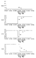
- the power-up reset signal 124 on the power-up reset line 96 makes a low-to-high transition 126. This sets both of the latches.
- a first conversion start pulse 128 on the conversion start line 116 then propagates through to the output of the third inverter 122, where it serves as a calibration start pulse 138 which initiates a first calibration. This calibration takes approximately 32 milliseconds, which provides sufficient time for the reference to settle.
- the calibration circuit provides a pulse 136 in the end of calibration signal 134 on the end of calibration line 88. This pulse resets the first latch (edge 144).
- the next conversion start pulse 129 then initiates a second calibration. This overwrites any results stored from the first calibration and provides accurate results, since the reference voltage has now settled.
- the calibration circuit begins this second calibration, it provides a start of calibration signal on the start of calibration line 102, and this resets the second latch (edge 148).
- a write control register signal is provided on the write control register signal line 90 during operation of the power-up circuit 80, it will stop the power-up calibration sequence. This will allow a user to perform a conversion, even though it may be inaccurate, immediately after power-up of the circuit.
- the write register signal reflects any writing to the control register, and can be derived from the read/write line 29.
- the calibration circuit 14 needs to generate four status signals for the alternative power-up control circuit 80. These include the start of calibration signal, the end of calibration signal 134, and the calibration in progress signal 132. The circuitry used to derive these signals is not shown, so as not to obfuscate the invention, as its design would be straightforward to one of skill in the art.
- the power-up reset signal 126 can be generated by a small on-chip delay circuit.
- the optional calibration pin 84 can be used to initiate a calibration either during operation of the power-up control circuit, or thereafter.
- the power-up delay could be determined by an on-chip counter, or other on-chip circuitry. Such circuitry can be designed to match the settling characteristics of the reference.
Landscapes
- Engineering & Computer Science (AREA)
- Theoretical Computer Science (AREA)
- Analogue/Digital Conversion (AREA)
Description
Claims (8)
- A circuit for calibrating an analog/digital converter (12) in an integrated circuit (10) comprising:characterised in that the power-up delay means includes means for deriving the duration of a delay of the delayed signal from the means for deriving a reference.means (18) for providing power to the integrated circuit, including the analog/digital converter;power-up delay means (30,34) on the integrated circuit for generating a signal delayed from power-up of the integrated circuit;means (36) responsive to the power-up delay means for initiating a calibration of the analog/digital converter upon detecting the delayed signal;means (26) for deriving a reference on the integrated circuit; and,
- The analog/digital converter of claim 1 characterised in that the analog/digital converter is a charge-redistribution analog/digital converter having an analog input pin (24) and a digital data output port.
- The analog/digital converter of any previous claim further characterised by a power control circuit (16) for automatically placing the circuit in an operating mode upon power-up that keeps the integrated circuit in a shutdown mode when the integrated circuit is not converting or calibrating.
- The analog/digital converter of any previous claim characterised in that the means for deriving a reference includes an on-chip voltage reference and an on-chip bias current source, and wherein the power-up delay circuit is operatively connected to the on-chip current source to derive the delay duration therefrom.
- The analog/digital converter of any previous claim characterised in that the power-up delay circuit is constructed and adapted to operate without any external calibration pin (32) on the integrated circuit.
- The analog/digital converter of any previous claim characterised in that the power-up delay means is adapted to derive the delay duration from a capacitor (34) external to the integrated circuit, said capacitor being charged by the means for deriving a reference.
- The analog/digital converter of any previous claim further characterised by means for initiating a calibration of the analog/digital converter in response to a signal supplied externally to the integrated circuit on a calibration input pin (32).
- A method of calibrating an analog/digital converter (12) in an integrated circuit (10), comprising the steps of:characterised by deriving a reference on the integrated circuit, from the providing of power; andproviding power to the integrated circuit from an external power supply to a power pin (23) on the integrated circuit;generating a delayed signal, said signal being delayed from the occurrence of the step of providing power from the external power supply to the power pin (23) on the integrated circuit by a power-up delay circuit on the integrated circuit;initiating, by a calibration circuit on the integrated circuit, a calibration of an analog/digital converter on the integrated circuit upon detecting the delayed signal generated in the generating step;deriving the duration of the delay from the reference.
Applications Claiming Priority (3)
| Application Number | Priority Date | Filing Date | Title |
|---|---|---|---|
| US374169 | 1995-01-18 | ||
| US08/374,169 US5668551A (en) | 1995-01-18 | 1995-01-18 | Power-up calibration of charge redistribution analog-to-digital converter |
| PCT/US1996/000698 WO1996022632A1 (en) | 1995-01-18 | 1996-01-18 | Power-up calibration of charge redistribution analog-to-digital converter |
Publications (2)
| Publication Number | Publication Date |
|---|---|
| EP0804831A1 EP0804831A1 (en) | 1997-11-05 |
| EP0804831B1 true EP0804831B1 (en) | 1999-08-11 |
Family
ID=23475615
Family Applications (1)
| Application Number | Title | Priority Date | Filing Date |
|---|---|---|---|
| EP96903555A Expired - Lifetime EP0804831B1 (en) | 1995-01-18 | 1996-01-18 | Power-up calibration of charge redistribution analog-to-digital converter |
Country Status (5)
| Country | Link |
|---|---|
| US (1) | US5668551A (en) |
| EP (1) | EP0804831B1 (en) |
| JP (2) | JPH11506573A (en) |
| DE (1) | DE69603708T2 (en) |
| WO (1) | WO1996022632A1 (en) |
Families Citing this family (24)
| Publication number | Priority date | Publication date | Assignee | Title |
|---|---|---|---|---|
| JPH09275191A (en) * | 1996-02-08 | 1997-10-21 | Fujitsu Ltd | Semiconductor integrated circuit and circuit device using the same |
| IT1303209B1 (en) | 1998-12-03 | 2000-10-30 | Cselt Centro Studi Lab Telecom | DEVICE FOR COMPENSATION OF VARIATIONS OF PROCESS AND OPERATIONAL PARAMETERS IN INTEGRATED CIRCUITS IN CMOS TECHNOLOGY |
| US6369740B1 (en) | 1999-10-22 | 2002-04-09 | Eric J. Swanson | Programmable gain preamplifier coupled to an analog to digital converter |
| US6590517B1 (en) | 1999-10-22 | 2003-07-08 | Eric J. Swanson | Analog to digital conversion circuitry including backup conversion circuitry |
| US6414619B1 (en) | 1999-10-22 | 2002-07-02 | Eric J. Swanson | Autoranging analog to digital conversion circuitry |
| US6310518B1 (en) | 1999-10-22 | 2001-10-30 | Eric J. Swanson | Programmable gain preamplifier |
| US6681332B1 (en) * | 2000-03-13 | 2004-01-20 | Analog Devices, Inc. | System and method to place a device in power down modes/states and restore back to first mode/state within user-controlled time window |
| US6445319B1 (en) | 2000-05-10 | 2002-09-03 | Texas Instruments Incorporated | Analog to digital converter circuit |
| US6768222B1 (en) * | 2000-07-11 | 2004-07-27 | Advanced Micro Devices, Inc. | System and method for delaying power supply power-up |
| US7031683B2 (en) * | 2001-01-12 | 2006-04-18 | Silicon Laboratories Inc. | Apparatus and methods for calibrating signal-processing circuitry |
| US6384760B1 (en) | 2001-05-30 | 2002-05-07 | Agilent Technologies, Inc. | Analog-to-digital converter |
| US6433713B1 (en) | 2001-05-31 | 2002-08-13 | Agilent Technologies, Inc. | Calibration of analog-to-digital converters |
| JP3623205B2 (en) * | 2002-03-22 | 2005-02-23 | 株式会社半導体理工学研究センター | Analog / digital converter |
| US6864814B1 (en) * | 2002-06-27 | 2005-03-08 | Qlogic Corporation | System and method for improving dynamic range of analog-to digital converters |
| US20040207864A1 (en) * | 2003-04-18 | 2004-10-21 | Combs Steven Donald | Method for operating a printer and method for operating a printer controller |
| KR100570978B1 (en) * | 2004-02-20 | 2006-04-13 | 삼성에스디아이 주식회사 | Organic electroluminescent display device using surface modified organic film layer and manufacturing method thereof |
| US7061413B2 (en) * | 2004-08-25 | 2006-06-13 | Micron Technology, Inc. | Analog to digital conversion with offset cancellation |
| US7605723B2 (en) * | 2004-12-14 | 2009-10-20 | Cirrus Logic, Inc. | Circuits and methods for implementing mode selection in multiple-mode integrated circuits |
| US8384559B2 (en) | 2010-04-13 | 2013-02-26 | Silicon Laboratories Inc. | Sensor device with flexible interface and updatable information store |
| US8643168B1 (en) * | 2012-10-16 | 2014-02-04 | Lattice Semiconductor Corporation | Integrated circuit package with input capacitance compensation |
| CN104124968B (en) * | 2014-08-06 | 2017-12-29 | 西安电子科技大学 | A kind of clock duty cycle calibration circuit for flow-line modulus converter |
| US20210066214A1 (en) * | 2019-08-27 | 2021-03-04 | Texas Instruments Incorporated | Integrated circuit devices with capacitors |
| US11476863B2 (en) | 2019-11-08 | 2022-10-18 | Analog Devices International Unlimited Company | Signal dependent reconfigurable data acquisition system |
| US11664062B2 (en) * | 2020-07-24 | 2023-05-30 | Advanced Micro Devices, Inc. | Memory calibration system and method |
Family Cites Families (77)
| Publication number | Priority date | Publication date | Assignee | Title |
|---|---|---|---|---|
| US3286232A (en) * | 1961-11-03 | 1966-11-15 | Gen Electric | Digital comparator classifying device |
| JPS5650232B2 (en) * | 1972-11-15 | 1981-11-27 | ||
| US3988689A (en) * | 1975-02-07 | 1976-10-26 | National Semiconductor Corporation | Offset corrected amplifier |
| NL7512886A (en) * | 1975-11-04 | 1977-05-06 | Hollandse Signaalapparaten Bv | ANALOG-DIGITAL CONVERTER. |
| GB1518558A (en) * | 1976-03-24 | 1978-07-19 | Gen Instr Microelect | Analogue-digital conversion |
| US4077035A (en) * | 1976-05-10 | 1978-02-28 | International Business Machines Corporation | Two-stage weighted capacitor circuit for analog-to-digital and digital-to-analog converters |
| US4070666A (en) * | 1976-06-21 | 1978-01-24 | General Electric Company | Automatic polarity sensing analog-to-digital converter |
| JPS5953727B2 (en) * | 1977-04-06 | 1984-12-26 | 株式会社日立製作所 | DA converter with correction circuit |
| NL7712273A (en) * | 1977-11-08 | 1979-05-10 | Philips Nv | METHOD AND DEVICE FOR AUTOMATIC CALIBRATION OF AN ANALOGUE-DIGITAL CONVERTER. |
| US4144527A (en) * | 1977-08-18 | 1979-03-13 | General Electric Company | Dual-slope analog to digital converter |
| US4129863A (en) * | 1977-10-03 | 1978-12-12 | Regents Of The University Of California | Weighted capacitor analog/digital converting apparatus and method |
| US4180807A (en) * | 1977-11-17 | 1979-12-25 | General Electric Company | Charge transfer circuit with voltage threshold compensating means |
| US4191900A (en) * | 1978-01-27 | 1980-03-04 | National Semiconductor Corporation | Precision plural input voltage amplifier and comparator |
| US4190854A (en) * | 1978-02-15 | 1980-02-26 | National Semiconductor Corporation | Trim structure for integrated capacitors |
| SU919076A1 (en) * | 1978-12-20 | 1982-04-07 | Особое Конструкторское Бюро Технической Кибернетики Ленинградского Ордена Ленина Политехнического Института Им.М.И.Калинина | Analogue-digital converter with automatic calibration |
| US4222107A (en) * | 1979-01-22 | 1980-09-09 | Burr-Brown Research Corporation | Method and apparatus for automatically calibrating a digital to analog converter |
| JPS55100744A (en) * | 1979-01-29 | 1980-07-31 | Hitachi Ltd | Da converter with correction circuit |
| US4335371A (en) * | 1979-04-09 | 1982-06-15 | National Semiconductor Corporation | Digital error correcting trimming in an analog to digital converter |
| US4272760A (en) * | 1979-04-10 | 1981-06-09 | Burr-Brown Research Corporation | Self-calibrating digital to analog conversion system and method |
| US4308524A (en) * | 1979-06-05 | 1981-12-29 | Harrison Systems, Inc. | Fast high resolution predictive analog-to-digital converter with error correction |
| US4250494A (en) * | 1979-07-09 | 1981-02-10 | General Electric Company | Charge transfer analog-to-digital converter with precise charge control |
| US4348658A (en) * | 1980-05-09 | 1982-09-07 | Motorola, Inc. | Analog-to-digital converter using half range technique |
| US4295089A (en) * | 1980-06-12 | 1981-10-13 | Gte Laboratories Incorporated | Methods of and apparatus for generating reference voltages |
| US4385286A (en) * | 1980-07-18 | 1983-05-24 | American Microsystems, Inc. | Use of single reference voltage for analog to digital or digital to analog conversion of bipolar signals |
| US4517549A (en) * | 1980-08-25 | 1985-05-14 | Oki Electric Industry Co., Ltd. | Weighted capacitor analogue-digital converters |
| US4399426A (en) * | 1981-05-04 | 1983-08-16 | Tan Khen Sang | On board self-calibration of analog-to-digital and digital-to-analog converters |
| US4439693A (en) * | 1981-10-30 | 1984-03-27 | Hughes Aircraft Co. | Sample and hold circuit with improved offset compensation |
| US4458237A (en) * | 1981-11-03 | 1984-07-03 | Texas Instruments Incorporated | Combination of an analog to digital converter with a sampling switch error correction circuit and least significant bit circuit |
| US4429282A (en) * | 1982-02-08 | 1984-01-31 | Bell Telephone Laboratories, Incorporated | Offset-nulled sample-and-hold amplifier |
| US4553052A (en) * | 1982-04-23 | 1985-11-12 | Nec Corporation | High speed comparator circuit with input-offset compensation function |
| JPS59151510A (en) * | 1983-02-18 | 1984-08-30 | Hitachi Ltd | C-mos load type amplifier |
| JPS59219076A (en) * | 1983-05-27 | 1984-12-10 | Hitachi Ltd | Ghost eliminating device provided with c-mos load type amplifier |
| US4543953A (en) * | 1983-07-18 | 1985-10-01 | Cordis Corporation | Analog telemetry system for biomedical implant |
| US4542354A (en) * | 1983-08-01 | 1985-09-17 | Robinton Products, Inc. | Delta-sigma pulse modulator with offset compensation |
| US4620179A (en) * | 1983-08-29 | 1986-10-28 | Harris Corporation | Method for successive approximation A/D conversion |
| US4555668A (en) * | 1983-10-14 | 1985-11-26 | American Microsystems, Inc. | Gain amplifier |
| JPS60124125A (en) * | 1983-12-08 | 1985-07-03 | Ishida Scales Mfg Co Ltd | High speed analog/digital conversion circuit of multi-input signal |
| US4641129A (en) * | 1984-02-09 | 1987-02-03 | Intersil, Inc. | Analog to digital converter with parallel and successive approximation stages |
| US4654815A (en) * | 1985-02-07 | 1987-03-31 | Texas Instruments Incorporated | Analog signal conditioning and digitizing integrated circuit |
| DE3521224A1 (en) * | 1985-06-13 | 1986-12-18 | Robert Bosch Gmbh, 7000 Stuttgart | ANALOG / DIGITAL CONVERTER |
| US4709225A (en) * | 1985-12-16 | 1987-11-24 | Crystal Semiconductor Corporation | Self-calibration method for capacitors in a monolithic integrated circuit |
| DE3603833A1 (en) * | 1986-02-07 | 1987-08-13 | Ant Nachrichtentech | DEVICE FOR ANALOG / DIGITAL CONVERSION OF ELECTRICAL ANALOG SIGNALS |
| US4700174A (en) * | 1986-05-12 | 1987-10-13 | Westinghouse Electric Corp. | Analog signal processor |
| JP2559032B2 (en) * | 1986-09-13 | 1996-11-27 | 富士通株式会社 | Differential amplifier circuit |
| FR2604840B1 (en) * | 1986-10-07 | 1988-12-09 | Efcis | DIFFERENTIAL ANALOG-TO-DIGITAL CONVERTER WITH SWITCHED CAPACITIES |
| US4881044A (en) * | 1987-01-16 | 1989-11-14 | Hitachi, Ltd. | Amplifying circuit |
| JPH0810830B2 (en) * | 1987-03-04 | 1996-01-31 | 株式会社東芝 | Analog-digital converter |
| IT1214249B (en) * | 1987-06-10 | 1990-01-10 | Sgs Microelettronica Spa | HIGH PERFORMANCE CMOS OPERATIONAL AMPLIFIER. |
| JPH0734541B2 (en) * | 1987-07-27 | 1995-04-12 | 日本電気株式会社 | Successive approximation type analog-digital conversion system |
| US4831381A (en) * | 1987-08-11 | 1989-05-16 | Texas Instruments Incorporated | Charge redistribution A/D converter with reduced small signal error |
| US4803462A (en) * | 1987-08-11 | 1989-02-07 | Texas Instruments Incorporated | Charge redistribution A/D converter with increased common mode rejection |
| US4804960A (en) * | 1987-10-08 | 1989-02-14 | Analog Deivces, Incorporated | Sub-ranging A/D converter with improved error correction |
| US4883987A (en) * | 1988-05-04 | 1989-11-28 | Texas Instruments Incorporated | Comparator circuit having a fast recovery time |
| US4833418A (en) * | 1988-09-01 | 1989-05-23 | Archive Corporation | Compensation circuit for nullifying differential offset voltage and regulating common mode voltage of differential signals |
| DE3850879D1 (en) * | 1988-09-30 | 1994-09-01 | Siemens Ag | Self-calibrating A / D and D / A converter. |
| US5047665A (en) * | 1989-02-08 | 1991-09-10 | Burr-Brown Corporation | Low noise, low offset, high speed CMOS differential amplifier |
| US4982194A (en) * | 1989-04-20 | 1991-01-01 | Harris Corporation | Back-sampling charge redistribution analog to digital converter |
| US5014055A (en) * | 1989-05-24 | 1991-05-07 | Harris Corporation | Analog-to-digital converter and method of use utilizing charge redistribution |
| US5036322A (en) * | 1989-06-02 | 1991-07-30 | Analog Devices, Inc. | Digital-to-analog converters with improved linearity |
| EP0407675A1 (en) * | 1989-07-13 | 1991-01-16 | IRD MECHANALYSIS, Inc. | Shaft synchronous balancing apparatus |
| US5043732A (en) * | 1989-09-26 | 1991-08-27 | Analog Devices, Inc. | Analog-to-digital converter employing a pipeline multi-stage architecture |
| IT1236879B (en) * | 1989-11-22 | 1993-04-26 | Sgs Thomson Microelectronics | COMPARATOR ELECTRONIC CIRCUIT |
| US5006853A (en) * | 1990-02-12 | 1991-04-09 | Texas Instruments Incorporated | Hysteresis insensitive analog to digital converter system using a coarse comparator and a fine comparator |
| US5016014A (en) * | 1990-06-14 | 1991-05-14 | Ncr Corporation | High accuracy analog-to-digital converter with rail-to-rail reference and input voltage ranges |
| US5220206A (en) * | 1990-06-29 | 1993-06-15 | Analog Devices, Inc. | Control apparatus with improved recovery from power reduction, and storage device therefor |
| US5138319A (en) * | 1990-08-30 | 1992-08-11 | Harris Corporation | Two stage a/d converter utilizing dual multiplexed converters with a common converter |
| US5233180A (en) * | 1990-08-30 | 1993-08-03 | Fuji Electric Co., Ltd. | Light sensor having an integration circuit |
| US5184130A (en) * | 1991-02-08 | 1993-02-02 | Analog Devices, Incorporated | Multi-stage A/D converter |
| US5124663A (en) * | 1991-03-04 | 1992-06-23 | Motorola, Inc. | Offset compensation CMOS operational amplifier |
| US5272395A (en) * | 1991-04-05 | 1993-12-21 | Analog Devices, Inc. | CMOS strobed comparator |
| US5248974A (en) * | 1991-06-27 | 1993-09-28 | Texas Instruments Incorporated | Dielectric relaxation correction circuit for charge-redistribution a/d converters |
| US5235333A (en) * | 1992-03-05 | 1993-08-10 | Burr-Brown Corporation | Hysteresis-insensitive single-comparator successive approximation analog-to-digital converter |
| US5258761A (en) * | 1992-03-16 | 1993-11-02 | Bahram Fotouhi | High resolution charge-redistribution A/D converter |
| US5245223A (en) * | 1992-03-17 | 1993-09-14 | Hewlett-Packard Company | CMOS latching comparator |
| JPH05342438A (en) * | 1992-06-09 | 1993-12-24 | Toshiba Corp | Automatic ticket examining device |
| US5381148A (en) * | 1993-07-12 | 1995-01-10 | Analog Devices, Inc. | Method and apparatus for calibrating a gain control circuit |
| JP3748886B2 (en) * | 1994-04-29 | 2006-02-22 | アナログ・デバイセス・インコーポレーテッド | Charge redistribution analog-to-digital converter with system calibration |
-
1995
- 1995-01-18 US US08/374,169 patent/US5668551A/en not_active Expired - Lifetime
-
1996
- 1996-01-18 EP EP96903555A patent/EP0804831B1/en not_active Expired - Lifetime
- 1996-01-18 JP JP8522387A patent/JPH11506573A/en active Pending
- 1996-01-18 WO PCT/US1996/000698 patent/WO1996022632A1/en not_active Ceased
- 1996-01-18 DE DE69603708T patent/DE69603708T2/en not_active Expired - Lifetime
-
2006
- 2006-07-26 JP JP2006203296A patent/JP2006325251A/en active Pending
Also Published As
| Publication number | Publication date |
|---|---|
| EP0804831A1 (en) | 1997-11-05 |
| WO1996022632A1 (en) | 1996-07-25 |
| DE69603708T2 (en) | 1999-12-23 |
| JP2006325251A (en) | 2006-11-30 |
| US5668551A (en) | 1997-09-16 |
| DE69603708D1 (en) | 1999-09-16 |
| JPH11506573A (en) | 1999-06-08 |
Similar Documents
| Publication | Publication Date | Title |
|---|---|---|
| US5668551A (en) | Power-up calibration of charge redistribution analog-to-digital converter | |
| US7196526B2 (en) | Matched delay line voltage converter | |
| US5760720A (en) | Digital trimming of on-chip analog components | |
| US6009487A (en) | Method and apparatus for setting a current of an output driver for the high speed bus | |
| KR930005838B1 (en) | Ic with processing circuit of digital and analogue signal | |
| US5914681A (en) | Fast wakeup biasing circuit for analog-to-digital converter | |
| US6894501B1 (en) | Selecting multiple settings for an integrated circuit function using a single integrated circuit terminal | |
| JP4007843B2 (en) | Digitally controlled adaptive driver and method for adjusting drive capability thereof | |
| US7327174B2 (en) | Fast locking mechanism for delay lock loops and phase lock loops | |
| US11231732B1 (en) | Pre-charge management for power-managed voltage references | |
| US7586331B2 (en) | Self-adaptive output buffer based on charge sharing | |
| US8618869B2 (en) | Fast power-on bias circuit | |
| US7498891B2 (en) | Method for calibration of an oscillator for a microcontroller chip operation | |
| KR100606896B1 (en) | Voltage supply sequence automatic control device and method | |
| US20250158631A1 (en) | Methods and systems of utilizing analog-to-digital converter (adc) for multiply-accumulator (mac) | |
| US20250392151A1 (en) | Circuitry for charging a bootstrap capacitor | |
| INPUTS | AD7811/AD7812–SPECIFICATIONS | |
| JP3254897B2 (en) | A / D converter | |
| US20070021846A1 (en) | Button device | |
| GRADE | ADuC814–SPECIFICATIONS | |
| Dual-In-Line et al. | Key Specifications | |
| CN118433956A (en) | LED Driver EMI Mitigation | |
| CN122026891A (en) | Pin multiplexing circuit of data conversion chip | |
| Grade et al. | AD977–SPECIFICATIONS (–40 C to | |
| Specifications | ADC0808/ADC0809 8-Bit µP Compatible A/D Converters with 8-Channel Multiplexer |
Legal Events
| Date | Code | Title | Description |
|---|---|---|---|
| PUAI | Public reference made under article 153(3) epc to a published international application that has entered the european phase |
Free format text: ORIGINAL CODE: 0009012 |
|
| 17P | Request for examination filed |
Effective date: 19970818 |
|
| AK | Designated contracting states |
Kind code of ref document: A1 Designated state(s): DE FR GB |
|
| 17Q | First examination report despatched |
Effective date: 19971024 |
|
| GRAG | Despatch of communication of intention to grant |
Free format text: ORIGINAL CODE: EPIDOS AGRA |
|
| GRAG | Despatch of communication of intention to grant |
Free format text: ORIGINAL CODE: EPIDOS AGRA |
|
| GRAH | Despatch of communication of intention to grant a patent |
Free format text: ORIGINAL CODE: EPIDOS IGRA |
|
| GRAH | Despatch of communication of intention to grant a patent |
Free format text: ORIGINAL CODE: EPIDOS IGRA |
|
| GRAA | (expected) grant |
Free format text: ORIGINAL CODE: 0009210 |
|
| AK | Designated contracting states |
Kind code of ref document: B1 Designated state(s): DE FR GB |
|
| REF | Corresponds to: |
Ref document number: 69603708 Country of ref document: DE Date of ref document: 19990916 |
|
| ET | Fr: translation filed | ||
| PLBE | No opposition filed within time limit |
Free format text: ORIGINAL CODE: 0009261 |
|
| STAA | Information on the status of an ep patent application or granted ep patent |
Free format text: STATUS: NO OPPOSITION FILED WITHIN TIME LIMIT |
|
| 26N | No opposition filed | ||
| REG | Reference to a national code |
Ref country code: GB Ref legal event code: IF02 |
|
| PGFP | Annual fee paid to national office [announced via postgrant information from national office to epo] |
Ref country code: DE Payment date: 20140115 Year of fee payment: 19 |
|
| PGFP | Annual fee paid to national office [announced via postgrant information from national office to epo] |
Ref country code: FR Payment date: 20140108 Year of fee payment: 19 |
|
| PGFP | Annual fee paid to national office [announced via postgrant information from national office to epo] |
Ref country code: GB Payment date: 20150114 Year of fee payment: 20 |
|
| REG | Reference to a national code |
Ref country code: DE Ref legal event code: R119 Ref document number: 69603708 Country of ref document: DE |
|
| PG25 | Lapsed in a contracting state [announced via postgrant information from national office to epo] |
Ref country code: DE Free format text: LAPSE BECAUSE OF NON-PAYMENT OF DUE FEES Effective date: 20150801 |
|
| REG | Reference to a national code |
Ref country code: FR Ref legal event code: ST Effective date: 20150930 |
|
| PG25 | Lapsed in a contracting state [announced via postgrant information from national office to epo] |
Ref country code: FR Free format text: LAPSE BECAUSE OF NON-PAYMENT OF DUE FEES Effective date: 20150202 |
|
| REG | Reference to a national code |
Ref country code: GB Ref legal event code: PE20 Expiry date: 20160117 |
|
| PG25 | Lapsed in a contracting state [announced via postgrant information from national office to epo] |
Ref country code: GB Free format text: LAPSE BECAUSE OF EXPIRATION OF PROTECTION Effective date: 20160117 |