US6433713B1 - Calibration of analog-to-digital converters - Google Patents

Calibration of analog-to-digital converters Download PDF

Info

Publication number
US6433713B1
US6433713B1 US09/867,580 US86758001A US6433713B1 US 6433713 B1 US6433713 B1 US 6433713B1 US 86758001 A US86758001 A US 86758001A US 6433713 B1 US6433713 B1 US 6433713B1
Authority
US
United States
Prior art keywords
calibration
discharge
time
integrator
determining
Prior art date
Legal status (The legal status is an assumption and is not a legal conclusion. Google has not performed a legal analysis and makes no representation as to the accuracy of the status listed.)
Expired - Fee Related
Application number
US09/867,580
Inventor
Philip B. Fuhrman
Current Assignee (The listed assignees may be inaccurate. Google has not performed a legal analysis and makes no representation or warranty as to the accuracy of the list.)
Agilent Technologies Inc
Original Assignee
Agilent Technologies Inc
Priority date (The priority date is an assumption and is not a legal conclusion. Google has not performed a legal analysis and makes no representation as to the accuracy of the date listed.)
Filing date
Publication date
Application filed by Agilent Technologies Inc filed Critical Agilent Technologies Inc
Priority to US09/867,580 priority Critical patent/US6433713B1/en
Assigned to AGILENT TECHNOLOGIES, INC. reassignment AGILENT TECHNOLOGIES, INC. ASSIGNMENT OF ASSIGNORS INTEREST (SEE DOCUMENT FOR DETAILS). Assignors: FUHRMAN, PHILIP B.
Application granted granted Critical
Publication of US6433713B1 publication Critical patent/US6433713B1/en
Anticipated expiration legal-status Critical
Expired - Fee Related legal-status Critical Current

Links

Images

Classifications

    • HELECTRICITY
    • H03ELECTRONIC CIRCUITRY
    • H03MCODING; DECODING; CODE CONVERSION IN GENERAL
    • H03M1/00Analogue/digital conversion; Digital/analogue conversion
    • H03M1/10Calibration or testing
    • H03M1/1009Calibration
    • H03M1/1014Calibration at one point of the transfer characteristic, i.e. by adjusting a single reference value, e.g. bias or gain error
    • H03M1/1019Calibration at one point of the transfer characteristic, i.e. by adjusting a single reference value, e.g. bias or gain error by storing a corrected or correction value in a digital look-up table
    • HELECTRICITY
    • H03ELECTRONIC CIRCUITRY
    • H03MCODING; DECODING; CODE CONVERSION IN GENERAL
    • H03M1/00Analogue/digital conversion; Digital/analogue conversion
    • H03M1/12Analogue/digital converters
    • H03M1/50Analogue/digital converters with intermediate conversion to time interval
    • H03M1/52Input signal integrated with linear return to datum

Definitions

  • the present invention relates to the field of calibration. More specifically, the invention relates to calibrating analog-to-digital converters.
  • A/D converters accumulate errors during conversion of analog signals into digital format. For example, the precision of the components in A/D converters varies, which leads to errors in the conversion process. These errors are typically corrected by calibration.
  • a disadvantage of conventional calibration is the requirement for control logics dedicated to the calibration process, which increases the cost and complexity of conventional A/D converters.
  • a need exists for a calibration method for A/D converters that accurately reflects errors that occur during conversion of analog signals into digital format.
  • a need also exists for a calibration method of reduced cost and complexity.
  • the present invention satisfies the above needs and achieves other advantages not present in conventional devices.
  • an A/D converter is operable in either an analog-to-digital conversion mode, or in a calibration mode.
  • the A/D converter performs conversion processes during which analog input signals are converted into digital output signals.
  • the A/D converter performs a calibration process.
  • the A/D converter calculates a calibration factor. The calibration factor is used in conversion processes to correct for errors in the conversion processes.
  • the calibration process includes the steps of performing a plurality of first calibration cycles, and then performing a plurality of second calibration cycles.
  • the plurality of first calibration cycles include the steps of applying a secondary discharge current to an integrator for a first calibration time, and applying a primary discharge current to the integrator for a first discharge time.
  • a first discharge value is determined from the first calibration cycles.
  • the plurality of second calibration cycles also use the primary discharge current and the secondary discharge current, in order to determine a second discharge value.
  • a calibration factor is calculated from the first and second discharge values.
  • the first and second discharge values are a function of the ratio of the primary discharge current to the secondary discharge current. Therefore, an external reference is not required. In addition, it is not necessary to calculate the actual values of the primary and secondary discharge currents, or of the corresponding reference voltages used to generate the primary and secondary discharge currents, because only the ratio between the values is required to calculate the calibration ratio.
  • the reference voltages may be the same references used during conversion operations of the A/D converter. Therefore, the calibration result accurately reflects the errors arising during conversion operations of the A/D converter.
  • FIG. 1 is a schematic diagram of an analog-to-digital convert according to an embodiment of the present invention.
  • FIG. 2 is a state diagram for the A/D converter of FIG. 1 .
  • FIG. 3 illustrates a method of operating the A/D converter of FIG. 1 in a conversion mode.
  • FIG. 4 illustrates voltage on an integration capacitor and a discharge control in the conversion mode.
  • FIG. 5 illustrates a method of operating the A/D converter in a calibration mode.
  • FIG. 6 illustrates a method of operating the A/D converter in a first and a second calibration cycle.
  • FIG. 7 illustrates voltage on an integration capacitor and a discharge control in the first calibration cycle.
  • FIG. 8 illustrates voltage on an integration capacitor and a discharge control in the second calibration cycle.
  • FIG. 1 illustrates an analog-to-digital (A/D) converter 10 according to an embodiment of the present invention.
  • the AID converter 10 is a continuously integrating, multislope A/D converter.
  • the A/ID converter 10 includes an integrator 12 which is comprised of an operational amplifier 13 and an integration capacitor C.
  • the operational amplifier 13 has a non-inverting input 14 , an inverting input 16 , and an output 18 .
  • the inverting input 16 is coupled to a small reference voltage ⁇ VREF through a resistor R 1 and a switch SW 1 , and coupled to a large reference voltage N ⁇ VREF through a resistor R 2 and a switch SW 2 .
  • the input voltage VIN is coupled to the input 16 through a resistor R 3 and a switch SW 3 .
  • the non-inverting input 14 is coupled to ground, and the output 18 is coupled to a non-inverting input 22 of a comparator 20 .
  • An inverting input 24 of the comparator 20 is coupled to ground, and an output 26 of the comparator 20 is coupled to a control logic 30 .
  • the control logic 30 is coupled to the switches SW 1 , SW 2 , SW 3 , and controls the opening and closing of the switches SW 1 , SW 2 , SW 3 .
  • a clock 40 is coupled to the control logic 30 to provide a time base to the control logic 30 .
  • the control logic 30 includes primary and secondary counters.
  • the outputs of the primary and secondary counters are coupled to a processor (not illustrated) of the A/D converter 10 .
  • the processor may be, for example, a central processing unit, a microprocessor, or other processing unit.
  • the processor uses the count 1 and count 2 values for A/D conversion of the input voltage VIN, and to perform calibration functions for the A/D converter 10 .
  • the A/D converter 10 is operable in two modes: a conversion mode and a calibration mode.
  • FIG. 2 illustrates a state diagram for the A/D converter 10 for both the conversion mode and the calibration mode.
  • the conversion mode the A/D converter 10 converts an unknown analog input signal VIN into a digital output signal.
  • the calibration mode the A/D converter 10 determines a calibration factor ⁇ to be applied during the conversion process to correct for errors in the conversion process.
  • the conversion process and the calibration process are synchronous, and both processes repeat over a fixed number of counts. In the exemplary embodiments discussed below, the conversion process and the calibration process repeat over a cycle of 2048 counts, although greater or fewer counts can be used.
  • the conversion mode and the calibration mode of operating the A/D converter 10 are similar, and the two modes can be carried out using similar logic.
  • the A/D converter 10 proceeds through states 1 - 7 , and returns to state 1 to begin a new conversion cycle.
  • the A/D converter 10 proceeds through states 1 - 4 , 8 , 9 , 7 , and returns to state 1 to begin a new calibration cycle.
  • the conversion process may be performed during specified periods. During these periods, the A/D converter 10 performs its primary function of converting analog signals into digital signals over a series of conversion cycles.
  • the A/D converter 10 can be programmed to operate in the calibration mode for selected intervals between periods of conversion. In the calibration mode, the A/D converter 10 executes a number of calibration cycles, and generates the calibration factor ⁇ . After the calibration process is complete, the A/D converter 10 reverts to the conversion mode. In the conversion mode, the A/D converter 10 utilizes the calibration factor ⁇ from the calibration process to correct for errors in the conversion process.
  • the conversion mode and the calibration mode are each discussed in detail below.
  • FIG. 3 is a flow chart illustrating a method of operating the A/D converter 10 in the conversion mode.
  • FIG. 4 illustrates voltage on the integration capacitor C, and a discharge control, during the conversion process.
  • the conversion process comprises a series of conversion cycles, each conversion cycle being represented by the closed conversion loop in FIG. 2 (states 1 - 7 , 1 ). Each conversion cycle can last, for example, for 2048 counts.
  • the conversion process begins at step S 10 by closing the switch SW 3 , which results in the application of an input current VIN/R 3 to the integrator 12 .
  • the controller 30 maintains the application of the input current VIN/R 3 throughout the conversion process.
  • Step S 10 begins state 1 .
  • the switches SW 1 and SW 2 are open, and no reference currents are applied to the integrator 12 .
  • the A/D converter 10 is maintained in state 1 for a time T 1 , during which time the charge on the integration capacitor C increases due to the application of the input current VIN/R 3 .
  • the increase in voltage on the integration capacitor C over time T 1 is illustrated by FIG. 4 .
  • step S 20 the switch SW 2 is closed, and a primary discharge current N ⁇ VREF/R 2 is applied to the inverting input 16 for a time T 2 .
  • Time T 2 is the primary discharge period for the integrator 12 , and states 2 - 4 all occur during time T 2 .
  • the switch SW 3 remains closed, and the combination of the input current VIN/R 3 and the primary discharge current N ⁇ VREF/R 2 discharges the integration capacitor C through ground.
  • FIG. 4 illustrates the drop in voltage on the integration capacitor C during T 2 .
  • the magnitude of the charge of the integration capacitor C decreases until an output signal X (see FIG. 1) from the operational amplifier 13 crosses zero, as detected by the comparator 20 in step S 30 .
  • the zero crossing of the signal X indicates zero voltage on the integration capacitor C, and corresponds to state 3 .
  • the SW 2 After the signal X crosses zero, the SW 2 remains closed, and a nonzero voltage accumulates on the integration capacitor C in step S 40 .
  • the accumulation of charge on the integration capacitor C corresponds to state 4 , which occurs at the end of the primary discharge period T 2 .
  • the switch SW 2 is maintained closed for a small, fixed time after the zero crossing, which may be on the order of, for example, 1-5% of the total conversion cycle time.
  • the primary counter 30 determines time T 2 as count 1 in FIG. 1 .
  • the time T 2 is the amount of time elapsed between step S 20 and S 30 , plus the fixed time amount of time that the primary discharge current is applied after the zero crossing.
  • step S 50 the control logic 30 opens the switch SW 2 for a time T 3 , disconnecting the primary discharge current from the integrator 12 .
  • the switch SW 3 remains closed.
  • the time T 3 during which time the A/D converter 10 is in state 5 , allows transients arising from current switching to die away.
  • the time T 3 may be a relatively short time, on the order of, for example, 5% of the total conversion cycle time.
  • step S 60 the switch SW 1 is closed for a time period of T 4 +T 5 , while a secondary discharge current ⁇ VREF/R 1 is applied to the integrator 12 through the resistor R 1 .
  • the time T 4 +T 5 corresponds to the secondary discharge period, or states 6 and 7 .
  • a secondary discharge current of ⁇ VREF/R 1 is applied to the integrator 12 .
  • the integrator 12 is discharged more slowly in the secondary discharge period than in the primary discharge period, because the secondary discharge current is smaller than the primary discharge current.
  • the primary discharge current would be 4 ⁇ VREF/R 2 .
  • the resistance of R 2 can be selected so that it is smaller than R 1 , for example, by a factor of 4. Therefore, in this example, the primary discharge current would be 16 times as great in magnitude as the secondary discharge current.
  • the ratio of primary to secondary discharge current can be referred to generally as ⁇ .
  • T 4 is the time required for the integration capacitor C charge to cross zero after applying the secondary discharge current.
  • the secondary counter determines time T 4 as count 2. Because the secondary discharge rate is approximately ⁇ fraction (1/16) ⁇ th of the primary discharge rate, the voltage change per count of the secondary counter is of approximately 16 times finer resolution than the primary counter during the primary discharge period.
  • step S 65 the processor calculates a time T 5 .
  • step S 70 the switch SW 1 remains closed for the time T 5 , and a nonzero voltage accumulates on the integration capacitor C during the time T 5 .
  • the time T 5 corresponds to state 7 .
  • State 7 serves the dual purpose of allowing a nonzero voltage to accumulate on the integration capacitor C after the zero crossing, and of providing a window to apply a correction time to the conversion process.
  • the time T 5 includes a fixed time period m, and a variable correction time ⁇ .
  • the correction time ⁇ is advantageous because errors in the VIN measurement may be introduced by mismatches in the primary and secondary discharge currents.
  • the ideal constant ratio ⁇ ⁇ 16. Errors arise from mismatches in the discharge currents that occur due to the limits of resolution of the resistors R 1 , R 2 , and other components in the A/D converter 10 . Because the A/D processor assumes the ideal ratio ⁇ when making the conversion calculation for VIN, failure to correct for errors during conversion can result in periodic nonlinearities in the conversion process.
  • mismatches in the primary and secondary discharge currents are compensated for by adding the variable correction time ⁇ to the fixed time m.
  • the correction time ⁇ is calculated using the calibration factor ⁇ calculated in the calibration process. The calculation of the calibration factor ⁇ will be discussed later with reference to FIGS. 5 and 6. The application of the correction time ⁇ to the conversion process in order to calculate T 5 is discussed below.
  • the integration capacitor C continues to discharge in state 7 .
  • the time that the A/D converter remains in state 7 is:
  • T 5 m+ ⁇ .
  • the correction time ⁇ can be positive or negative.
  • the value m is a nonzero value chosen to be greater than ⁇ , ensuring that T 5 is positive.
  • the correction time ⁇ is calculated according to the following general formula:
  • T 5 The calculation of T 5 is performed for each conversion cycle.
  • the calculation of the correction time ⁇ may be based on the immediately preceding time T 4 , or, it may be based on an average of T 4 values from a selected number of previous conversion cycles. In the latter case, the correction time would be calculated as:
  • the correction time ⁇ lags in the conversion process by one or more cycles.
  • the fractional values can be carried over into a subsequent conversion cycles using first order sigma-delta modulation or second order sigma-delta modulation.
  • the counts 1 (T 2 ) and 2 (T 4 ) measured during the primary and secondary discharge periods are output to the processor in step S 78 .
  • the counts 1 and 2 are used to convert VIN into digital format in the processor.
  • VIN is calculated by combining the times T 2 and T 4 , each time being weighted by the amplitude of its discharge current. In weighting T 2 and T 4 , T 4 is divided by the ideal ratio ⁇ , or, T 2 is multiplied by ideal ratio ⁇ .
  • the processor also applies post-conversion digital filtering, and other post-conversion signal processing.
  • the overall resolution of the AID converter 10 is determined by the smaller, secondary discharge current ⁇ VREF/R 2 , which meters smaller quanta of charge in the integrator 12 .
  • the dynamic range of the A/D converter 10 is determined by the larger, primary discharge current N ⁇ VREF/R 1 , which determines the maximum negative voltage that can be applied to the A/D converter while maintaining linear behavior of the integrator 12 .
  • the A/D converter 10 therefore achieves high resolution conversion of VIN, over a wide dynamic range, with low noise.
  • the above-described embodiment discloses reference voltages ⁇ VREF and N ⁇ VREF of opposite polarity. This feature provides flexibility to the control of the A/D converter 10 because the reference signals of opposite polarity can be used to balance the input signal VIN on either side of ground. Reference signals of opposite polarity also allow for continuous measurement of integration capacitor C charge from one side of ground, across ground, to the other side of ground. The A/D converter 10 therefore does not change its measurement characteristics in the vicinity of ground.
  • FIG. 5 illustrates a method of operating the A/D converter 10 in the calibration mode.
  • FIG. 6 illustrates the first and second calibration cycles of the calibration process.
  • FIG. 7 illustrates voltage on the integration capacitor C during the first calibration cycle, and
  • FIG. 8 illustrates voltage on the integration capacitor C during the second calibration cycle.
  • Calibration processes can be performed, for example, at predetermined intervals between conversion processes. Calibration can be performed more frequently if a higher degree of accuracy is desired for conversion processes, or in response to a change in environment, such as a change in temperature, or with increasing age of components within the A/D converter 10 .
  • a calibration process consists of performing a first calibration cycle for m iterations, and then performing a second calibration cycle for m iterations, and comparing discharge times from the first and second cycles in order to calculate a calibration factor ⁇ .
  • TC 2 1 discharge value from the m first calibration cycles
  • TCAL 1 known calibration time for the first calibration cycles
  • TCAL 2 known calibration time for the second calibration cycles
  • k 1 a constant, if necessary, due to scaling in implementation
  • m the number or iterations that the first and second calibration cycles are performed in the calibration process.
  • the discharge values TC 2 1 , TC 2 2 are determined by performing the first and second calibration cycles, respectively.
  • TCAL 1 and TCAL 2 are known values.
  • the calibration process will be discussed with reference to FIGS. 2 and 5.
  • the switch SW 3 Prior to calibration, the switch SW 3 is opened, and remains open throughout calibration.
  • the first calibration cycle is performed in step S 120 .
  • a first discharge time TC 2 is determined in step S 120 for the current iteration of the first calibration cycle (the first calibration cycle is discussed in detail with reference to FIG. 6 ).
  • Steps S 110 and S 120 are performed m times.
  • the first discharge value TC 2 1 is determined in step S 125 .
  • the first discharge value TC 2 1 can be calculated as a sum of the m first discharge times TC 2 from the m first calibration cycles, e.g., as a “cumulative” discharge time.
  • the value m can be any positive integer, including one.
  • step S 130 a second calibration cycle is performed.
  • step S 140 a second discharge time TC 2 is determined for each second calibration cycle.
  • the m values of second discharge time TC 2 are used to determine a second discharge value TC 2 2 , in step S 145 .
  • the second discharge value TC 2 2 may also be a cumulative discharge time for the m second calibration cycles.
  • the first calibration cycle begins in state 8 , with the switches SW 1 , SW 2 and SW 3 open.
  • the switches SW 1 and SW 2 remain open for a time TC 3 .
  • the switch SW 1 is closed for the first known calibration time TCAL 1 .
  • the first known calibration time TCAL 1 can be, for example, 1000 counts.
  • the application of the secondary discharge current ⁇ VREF/R 1 causes the integration capacitor C voltage to cross zero during TCAL 1 .
  • the time TCAL 1 corresponds to states 9 and 7 . It is not necessary to measure a zero crossing at state 7 .
  • the switch SW 1 is opened in step S 95 , disconnecting the secondary discharge current from the integrator 12 for a time TC 1 . This corresponds to state 1 in FIG. 2 .
  • step S 200 the switch SW 2 is closed, and the primary discharge current is applied to the inverting input 16 .
  • the primary discharge current of N ⁇ VREF/R 2 then discharges the integration capacitor C through ground, until the signal X crosses zero.
  • the zero crossing (state 3 ) is detected in step S 300 .
  • the zero crossing is illustrated in FIG. 7 .
  • step S 400 the switch 1 remains closed for a known time to accumulate a nonzero charge on the integration capacitor C, corresponding to state 4 in FIG. 2 .
  • step S 80 the control logic 30 opens the switch SW 2 , restoring the A/D converter 10 to state 8 .
  • the processor of the A/D converter 10 determines TC 2 as the time required for the capacitor C voltage to cross zero after applying the primary discharge current, plus the known time in step S 400 .
  • TC 2 is the discharge time for the first calibration cycle.
  • the A/D converter 10 After the first iteration of the first calibration cycle is complete, the A/D converter 10 performs the first calibration cycle repeatedly for m cycles.
  • the m first discharge times TC 2 from the m first calibration cycles are used to determine the cumulative, first discharge value TC 2 1 in step S 125 (FIG. 5 ).
  • m second calibration cycles are performed.
  • the second calibration cycles are also performed using the steps illustrated by FIG. 6, each second calibration cycle illustrated by FIG. 6 corresponding to an iteration of step S 130 in FIG. 5 .
  • a second discharge time TC 2 is determined (step S 140 of FIG. 5 ).
  • the cumulative, second discharge value TC 2 2 for the m second calibration cycles is determined.
  • the m second calibration cycles are performed using a calibration time TCAL 2 that is shorter than TCAL 1 .
  • the first and second discharge values TC 2 1 , TC 2 2 are used to calculate the calibration factor ⁇ as discussed above with reference to FIG. 5 .
  • the A/D converter 10 reverts to the conversion mode. In the conversion mode, the A/D) converter 10 utilizes the calibration factor ⁇ for calculation of the correction time ⁇ .
  • the first and second discharge values are a function of the ratio of the primary discharge current to the secondary discharge current.
  • This ratio dictates the zero crossing times that result from the applications of the primary discharge current, which are used to determine the discharge values.
  • the calibration factor can therefore be determined based upon the actual ratio of the primary discharge current to the secondary discharge current, and on the known calibration times. This feature eliminates the need for an external reference during calibration. In addition, it is not necessary to calculate the actual values of the primary and secondary discharge currents, or of the corresponding voltages ⁇ VREF and N ⁇ VREF, because only the ratio between the values is required to calculate the calibration ratio.
  • the small reference voltage ⁇ VREF and the large reference voltage N ⁇ VREF may be the references used during conversion operations of the A/D converter. Therefore, the calibration result accurately reflects the errors arising during conversion operations of the A/D converter.

Abstract

A multislope, continuously integrating analog-to-digital converter can operate in either a conversion mode or a calibration mode. During the calibration mode, a calibration factor is calculated for use during the conversion mode. When applied to the conversion mode, the calibration factor corrects for errors in the conversion process.

Description

TECHNICAL FIELD
The present invention relates to the field of calibration. More specifically, the invention relates to calibrating analog-to-digital converters.
BACKGROUND
Conventional analog-to-digital (A/D) converters accumulate errors during conversion of analog signals into digital format. For example, the precision of the components in A/D converters varies, which leads to errors in the conversion process. These errors are typically corrected by calibration. A disadvantage of conventional calibration is the requirement for control logics dedicated to the calibration process, which increases the cost and complexity of conventional A/D converters.
Conventional calibration processes may also utilize a separate calibration standard, such as an externally applied calibration voltage, in order to calibrate an A/D converter. However, calibration results in some converters, such as multislope converters, based on externally applied calibration voltages, do not reflect the errors that actually occur in an A/D converter during the conversion process. Also, in conventional multistage converters, a separate reference is required for each stage of the converter, which leads to further inaccuracies.
Therefore, a need exists for a calibration method for A/D converters that accurately reflects errors that occur during conversion of analog signals into digital format. A need also exists for a calibration method of reduced cost and complexity.
SUMMARY OF INVENTION
The present invention satisfies the above needs and achieves other advantages not present in conventional devices.
According to an aspect of the invention, an A/D converter is operable in either an analog-to-digital conversion mode, or in a calibration mode. In the conversion mode, the A/D converter performs conversion processes during which analog input signals are converted into digital output signals. In the calibration mode, the A/D converter performs a calibration process. During the calibration process, the A/D converter calculates a calibration factor. The calibration factor is used in conversion processes to correct for errors in the conversion processes.
The calibration process includes the steps of performing a plurality of first calibration cycles, and then performing a plurality of second calibration cycles. The plurality of first calibration cycles include the steps of applying a secondary discharge current to an integrator for a first calibration time, and applying a primary discharge current to the integrator for a first discharge time. A first discharge value is determined from the first calibration cycles. The plurality of second calibration cycles also use the primary discharge current and the secondary discharge current, in order to determine a second discharge value. A calibration factor is calculated from the first and second discharge values.
According to the above aspect, the first and second discharge values are a function of the ratio of the primary discharge current to the secondary discharge current. Therefore, an external reference is not required. In addition, it is not necessary to calculate the actual values of the primary and secondary discharge currents, or of the corresponding reference voltages used to generate the primary and secondary discharge currents, because only the ratio between the values is required to calculate the calibration ratio.
As a further advantage, the reference voltages may be the same references used during conversion operations of the A/D converter. Therefore, the calibration result accurately reflects the errors arising during conversion operations of the A/D converter.
Other aspects and advantages of the invention will be discussed with reference to the figures and to the detailed description of the preferred embodiments.
BRIEF DESCRIPTION OF THE FIGURES
FIG. 1 is a schematic diagram of an analog-to-digital convert according to an embodiment of the present invention.
FIG. 2 is a state diagram for the A/D converter of FIG. 1.
FIG. 3 illustrates a method of operating the A/D converter of FIG. 1 in a conversion mode.
FIG. 4 illustrates voltage on an integration capacitor and a discharge control in the conversion mode.
FIG. 5 illustrates a method of operating the A/D converter in a calibration mode.
FIG. 6 illustrates a method of operating the A/D converter in a first and a second calibration cycle.
FIG. 7 illustrates voltage on an integration capacitor and a discharge control in the first calibration cycle.
FIG. 8 illustrates voltage on an integration capacitor and a discharge control in the second calibration cycle.
DETAILED DESCRIPTION OF PREFERRED EMBODIMENTS
An analog-to-digital converter and a method of operating an analog-to-digital converter according to the present invention will be described below by way of preferred embodiments and with reference to the accompanying drawings.
FIG. 1 illustrates an analog-to-digital (A/D) converter 10 according to an embodiment of the present invention. The AID converter 10 is a continuously integrating, multislope A/D converter. The A/ID converter 10 includes an integrator 12 which is comprised of an operational amplifier 13 and an integration capacitor C. The operational amplifier 13 has a non-inverting input 14, an inverting input 16, and an output 18. The inverting input 16 is coupled to a small reference voltage −VREF through a resistor R1 and a switch SW1, and coupled to a large reference voltage N·VREF through a resistor R2 and a switch SW2. The input voltage VIN is coupled to the input 16 through a resistor R3 and a switch SW3. The non-inverting input 14 is coupled to ground, and the output 18 is coupled to a non-inverting input 22 of a comparator 20. An inverting input 24 of the comparator 20 is coupled to ground, and an output 26 of the comparator 20 is coupled to a control logic 30.
The control logic 30 is coupled to the switches SW1, SW2, SW3, and controls the opening and closing of the switches SW1, SW2, SW3. A clock 40 is coupled to the control logic 30 to provide a time base to the control logic 30.
The control logic 30 includes primary and secondary counters. The outputs of the primary and secondary counters are coupled to a processor (not illustrated) of the A/D converter 10. The processor may be, for example, a central processing unit, a microprocessor, or other processing unit. The processor uses the count 1 and count 2 values for A/D conversion of the input voltage VIN, and to perform calibration functions for the A/D converter 10.
The A/D converter 10 is operable in two modes: a conversion mode and a calibration mode. FIG. 2 illustrates a state diagram for the A/D converter 10 for both the conversion mode and the calibration mode. In the conversion mode, the A/D converter 10 converts an unknown analog input signal VIN into a digital output signal. In the calibration mode, the A/D converter 10 determines a calibration factor α to be applied during the conversion process to correct for errors in the conversion process. The conversion process and the calibration process are synchronous, and both processes repeat over a fixed number of counts. In the exemplary embodiments discussed below, the conversion process and the calibration process repeat over a cycle of 2048 counts, although greater or fewer counts can be used.
As illustrated by the state diagram, the conversion mode and the calibration mode of operating the A/D converter 10 are similar, and the two modes can be carried out using similar logic. In a conversion cycle, the A/D converter 10 proceeds through states 1-7, and returns to state 1 to begin a new conversion cycle. In a calibration cycle, the A/D converter 10 proceeds through states 1-4, 8, 9, 7, and returns to state 1 to begin a new calibration cycle.
The conversion process may be performed during specified periods. During these periods, the A/D converter 10 performs its primary function of converting analog signals into digital signals over a series of conversion cycles. The A/D converter 10 can be programmed to operate in the calibration mode for selected intervals between periods of conversion. In the calibration mode, the A/D converter 10 executes a number of calibration cycles, and generates the calibration factor α. After the calibration process is complete, the A/D converter 10 reverts to the conversion mode. In the conversion mode, the A/D converter 10 utilizes the calibration factor α from the calibration process to correct for errors in the conversion process. The conversion mode and the calibration mode are each discussed in detail below.
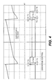
The conversion mode of the A/D converter 10 will now be discussed with reference to FIGS. 2-4. FIG. 3 is a flow chart illustrating a method of operating the A/D converter 10 in the conversion mode. FIG. 4 illustrates voltage on the integration capacitor C, and a discharge control, during the conversion process. The conversion process comprises a series of conversion cycles, each conversion cycle being represented by the closed conversion loop in FIG. 2 (states 1-7, 1). Each conversion cycle can last, for example, for 2048 counts.
Referring to FIGS. 2-4, the conversion process begins at step S10 by closing the switch SW3, which results in the application of an input current VIN/R3 to the integrator 12. The controller 30 maintains the application of the input current VIN/R3 throughout the conversion process. Step S10 begins state 1. In state 1, the switches SW1 and SW2 are open, and no reference currents are applied to the integrator 12. The A/D converter 10 is maintained in state 1 for a time T1, during which time the charge on the integration capacitor C increases due to the application of the input current VIN/R3. The increase in voltage on the integration capacitor C over time T1 is illustrated by FIG. 4.
In step S20, the switch SW2 is closed, and a primary discharge current N·VREF/R2 is applied to the inverting input 16 for a time T2. Time T2 is the primary discharge period for the integrator 12, and states 2-4 all occur during time T2. During time T2, the switch SW3 remains closed, and the combination of the input current VIN/R3 and the primary discharge current N·VREF/R2 discharges the integration capacitor C through ground. FIG. 4 illustrates the drop in voltage on the integration capacitor C during T2.
The magnitude of the charge of the integration capacitor C decreases until an output signal X (see FIG. 1) from the operational amplifier 13 crosses zero, as detected by the comparator 20 in step S30. The zero crossing of the signal X indicates zero voltage on the integration capacitor C, and corresponds to state 3.
After the signal X crosses zero, the SW2 remains closed, and a nonzero voltage accumulates on the integration capacitor C in step S40. The accumulation of charge on the integration capacitor C corresponds to state 4, which occurs at the end of the primary discharge period T2. The switch SW2 is maintained closed for a small, fixed time after the zero crossing, which may be on the order of, for example, 1-5% of the total conversion cycle time. The primary counter 30 determines time T2 as count 1 in FIG. 1. The time T2 is the amount of time elapsed between step S20 and S30, plus the fixed time amount of time that the primary discharge current is applied after the zero crossing.
In step S50, the control logic 30 opens the switch SW2 for a time T3, disconnecting the primary discharge current from the integrator 12. The switch SW3 remains closed. The time T3, during which time the A/D converter 10 is in state 5, allows transients arising from current switching to die away. The time T3 may be a relatively short time, on the order of, for example, 5% of the total conversion cycle time.
In step S60, the switch SW1 is closed for a time period of T4+T5, while a secondary discharge current −VREF/R1 is applied to the integrator 12 through the resistor R1. The time T4 +T5 corresponds to the secondary discharge period, or states 6 and 7. During the secondary discharge period, a secondary discharge current of −VREF/R1 is applied to the integrator 12. The integrator 12 is discharged more slowly in the secondary discharge period than in the primary discharge period, because the secondary discharge current is smaller than the primary discharge current. For example, if N=4, the primary discharge current would be 4·VREF/R2. The resistance of R2 can be selected so that it is smaller than R1, for example, by a factor of 4. Therefore, in this example, the primary discharge current would be 16 times as great in magnitude as the secondary discharge current. The ratio of primary to secondary discharge current can be referred to generally as λ.
The A/D converter 10 remains in state 6 until the comparator 20 detects a zero crossing of signal X in step S62. T4 is the time required for the integration capacitor C charge to cross zero after applying the secondary discharge current. The secondary counter determines time T4 as count 2. Because the secondary discharge rate is approximately {fraction (1/16)}th of the primary discharge rate, the voltage change per count of the secondary counter is of approximately 16 times finer resolution than the primary counter during the primary discharge period.
In step S65, the processor calculates a time T5. After the zero crossing, in step S70, the switch SW1 remains closed for the time T5, and a nonzero voltage accumulates on the integration capacitor C during the time T5. The time T5 corresponds to state 7. State 7 serves the dual purpose of allowing a nonzero voltage to accumulate on the integration capacitor C after the zero crossing, and of providing a window to apply a correction time to the conversion process. The time T5 includes a fixed time period m, and a variable correction time Δ.
The correction time Δ is advantageous because errors in the VIN measurement may be introduced by mismatches in the primary and secondary discharge currents. Ideally, the discharge currents have a constant ratio of λ=−N·R2/R1. In the exemplary embodiment discussed above, the ideal constant ratio λ=−16. Errors arise from mismatches in the discharge currents that occur due to the limits of resolution of the resistors R1, R2, and other components in the A/D converter 10. Because the A/D processor assumes the ideal ratio λ when making the conversion calculation for VIN, failure to correct for errors during conversion can result in periodic nonlinearities in the conversion process. According to the present invention, mismatches in the primary and secondary discharge currents are compensated for by adding the variable correction time Δ to the fixed time m. The correction time Δ is calculated using the calibration factor α calculated in the calibration process. The calculation of the calibration factor α will be discussed later with reference to FIGS. 5 and 6. The application of the correction time Δ to the conversion process in order to calculate T5 is discussed below.
After the comparator 20 detects a zero crossing of the signal X at state 6, the integration capacitor C continues to discharge in state 7. The time that the A/D converter remains in state 7 is:
T 5=m+Δ.
The correction time Δ can be positive or negative. The value m is a nonzero value chosen to be greater than Δ, ensuring that T5 is positive. The correction time Δ is calculated according to the following general formula:
Δ=T 4·α.
The calculation of T5 is performed for each conversion cycle.
The calculation of the correction time Δ may be based on the immediately preceding time T4, or, it may be based on an average of T4 values from a selected number of previous conversion cycles. In the latter case, the correction time would be calculated as:
Δ=T 4 avg·α.
When using an average T4 value, the correction time Δ lags in the conversion process by one or more cycles.
If the correction time Δ includes a fractional value of a clock cycle, the fractional values can be carried over into a subsequent conversion cycles using first order sigma-delta modulation or second order sigma-delta modulation.
The counts 1 (T2) and 2 (T4) measured during the primary and secondary discharge periods are output to the processor in step S78. The counts 1 and 2 are used to convert VIN into digital format in the processor. VIN is calculated by combining the times T2 and T4, each time being weighted by the amplitude of its discharge current. In weighting T2 and T4, T4 is divided by the ideal ratio λ, or, T2 is multiplied by ideal ratio λ. The processor also applies post-conversion digital filtering, and other post-conversion signal processing.
According to the above-described conversion process, the overall resolution of the AID converter 10 is determined by the smaller, secondary discharge current −VREF/R2, which meters smaller quanta of charge in the integrator 12. The dynamic range of the A/D converter 10 is determined by the larger, primary discharge current N·VREF/R1, which determines the maximum negative voltage that can be applied to the A/D converter while maintaining linear behavior of the integrator 12. The A/D converter 10 therefore achieves high resolution conversion of VIN, over a wide dynamic range, with low noise.
The above embodiment is described in the context of an ideal ratio of λ=−16. Other ratios, however, may achieve similar advantages. When choosing an ideal ratio λ, it is preferable to use a binary number because the conversion operation can use binary shifts when multiplying by λ.
The above-described embodiment discloses reference voltages −VREF and N·VREF of opposite polarity. This feature provides flexibility to the control of the A/D converter 10 because the reference signals of opposite polarity can be used to balance the input signal VIN on either side of ground. Reference signals of opposite polarity also allow for continuous measurement of integration capacitor C charge from one side of ground, across ground, to the other side of ground. The A/D converter 10 therefore does not change its measurement characteristics in the vicinity of ground.
The calibration factor a used in the conversion mode is calculated during a calibration process while the A/D converter 10 is in the calibration mode. The calibration mode of the A/D converter 10 will now be discussed with reference to FIGS. 2 and 5-8. FIG. 5 illustrates a method of operating the A/D converter 10 in the calibration mode. FIG. 6 illustrates the first and second calibration cycles of the calibration process. FIG. 7 illustrates voltage on the integration capacitor C during the first calibration cycle, and FIG. 8 illustrates voltage on the integration capacitor C during the second calibration cycle.
Calibration processes can be performed, for example, at predetermined intervals between conversion processes. Calibration can be performed more frequently if a higher degree of accuracy is desired for conversion processes, or in response to a change in environment, such as a change in temperature, or with increasing age of components within the A/D converter 10. A calibration process consists of performing a first calibration cycle for m iterations, and then performing a second calibration cycle for m iterations, and comparing discharge times from the first and second cycles in order to calculate a calibration factor α.
The calibration factor α is calculated according to the following formula: α = k1 · ( 1 - λ m · TC2 1 _ - TC2 2 _ TCAL1 - TCAL2 )
Figure US06433713-20020813-M00001
where:
λ=ideal ratio of primary discharge current to secondary discharge current
TC2 1 =discharge value from the m first calibration cycles
TC2 2 =discharge value from the m second calibration cycles
TCAL1=known calibration time for the first calibration cycles
TCAL2=known calibration time for the second calibration cycles
k1=a constant, if necessary, due to scaling in implementation
m=the number or iterations that the first and second calibration cycles are performed in the calibration process.
The discharge values TC2 1 , TC2 2 , are determined by performing the first and second calibration cycles, respectively. TCAL1 and TCAL2 are known values.
The calibration process will be discussed with reference to FIGS. 2 and 5. Prior to calibration, the switch SW3 is opened, and remains open throughout calibration. The first calibration cycle is performed in step S120. A first discharge time TC2 is determined in step S120 for the current iteration of the first calibration cycle (the first calibration cycle is discussed in detail with reference to FIG. 6). Steps S110 and S120 are performed m times. After m first discharge times TC2 are determined, the first discharge value TC2 1 is determined in step S125. The first discharge value TC2 1 can be calculated as a sum of the m first discharge times TC2 from the m first calibration cycles, e.g., as a “cumulative” discharge time. The value m can be any positive integer, including one.
After the m first calibration cycles are completed, the A/D converter 10 switches to execution of m second calibration cycles. In step S130, a second calibration cycle is performed. In step S140, a second discharge time TC2 is determined for each second calibration cycle. After m iterations of steps S130 and S140, the m values of second discharge time TC2 are used to determine a second discharge value TC2 2 , in step S145. The second discharge value TC2 2 may also be a cumulative discharge time for the m second calibration cycles.
In step S150, the calibration factor a is calculated using the formula: α = k1 · ( 1 - λ m · TC2 1 _ - TC2 2 _ TCAL1 - TCAL2 )
Figure US06433713-20020813-M00002
The first and second calibration cycles will now be discussed in detail with reference to FIGS. 2 and 5-7.
An iteration of the first calibration cycle, corresponding to step S110 in FIG. 5, is illustrated in FIG. 6. The first calibration cycle begins in state 8, with the switches SW1, SW2 and SW3 open. The switches SW1 and SW2 remain open for a time TC3. In step S90, the switch SW1 is closed for the first known calibration time TCAL1. The first known calibration time TCAL1 can be, for example, 1000 counts. As shown in FIG. 6, the application of the secondary discharge current −VREF/R1 causes the integration capacitor C voltage to cross zero during TCAL1. The time TCAL1 corresponds to states 9 and 7. It is not necessary to measure a zero crossing at state 7.
The switch SW1 is opened in step S95, disconnecting the secondary discharge current from the integrator 12 for a time TC1. This corresponds to state 1 in FIG. 2.
In step S200, the switch SW2 is closed, and the primary discharge current is applied to the inverting input 16. The primary discharge current of N·VREF/R2 then discharges the integration capacitor C through ground, until the signal X crosses zero. The zero crossing (state 3) is detected in step S300. The zero crossing is illustrated in FIG. 7. In step S400, the switch 1 remains closed for a known time to accumulate a nonzero charge on the integration capacitor C, corresponding to state 4 in FIG. 2. In step S80, the control logic 30 opens the switch SW2, restoring the A/D converter 10 to state 8. The processor of the A/D converter 10 determines TC2 as the time required for the capacitor C voltage to cross zero after applying the primary discharge current, plus the known time in step S400. TC2 is the discharge time for the first calibration cycle.
After the first iteration of the first calibration cycle is complete, the A/D converter 10 performs the first calibration cycle repeatedly for m cycles. The m first discharge times TC2 from the m first calibration cycles are used to determine the cumulative, first discharge value TC2 1 in step S125 (FIG. 5).
After performing m first calibration cycles, m second calibration cycles are performed. The second calibration cycles are also performed using the steps illustrated by FIG. 6, each second calibration cycle illustrated by FIG. 6 corresponding to an iteration of step S130 in FIG. 5. From each of the m second calibration cycles, a second discharge time TC2 is determined (step S140 of FIG. 5). From the m second discharge times TC2 , the cumulative, second discharge value TC2 2 for the m second calibration cycles is determined.
As shown in FIG. 8, the m second calibration cycles are performed using a calibration time TCAL2 that is shorter than TCAL1.
The first and second discharge values TC2 1 , TC2 2 are used to calculate the calibration factor α as discussed above with reference to FIG. 5. When the calibration process has been completed, and the calibration factor α calculated, the A/D converter 10 reverts to the conversion mode. In the conversion mode, the A/D) converter 10 utilizes the calibration factor α for calculation of the correction time Δ.
According to the present invention, the first and second discharge values are a function of the ratio of the primary discharge current to the secondary discharge current. This ratio dictates the zero crossing times that result from the applications of the primary discharge current, which are used to determine the discharge values. The calibration factor can therefore be determined based upon the actual ratio of the primary discharge current to the secondary discharge current, and on the known calibration times. This feature eliminates the need for an external reference during calibration. In addition, it is not necessary to calculate the actual values of the primary and secondary discharge currents, or of the corresponding voltages −VREF and N·VREF, because only the ratio between the values is required to calculate the calibration ratio.
As a further advantage, the small reference voltage −VREF and the large reference voltage N·VREF may be the references used during conversion operations of the A/D converter. Therefore, the calibration result accurately reflects the errors arising during conversion operations of the A/D converter.
While the present invention is described with reference to exemplary embodiments, it will be understood that many modifications will be readily apparent to those skilled in the art, and the present disclosure is intended to cover variations thereof.

Claims (20)

What is claimed is:
1. A method of calculating a calibration factor for an analog-to-digital converter, comprising:
performing at least one iteration of a first calibration cycle, comprising:
applying a secondary discharge current to an integrator for a first calibration time; and
applying a primary discharge current to the integrator for a first discharge time;
determining a first discharge value from the at least one iteration of the first calibration cycle;
performing at least one iteration of a second calibration cycle, comprising:
applying the secondary discharge current to the integrator for a second calibration time; and
applying the primary discharge current to the integrator for a second discharge time;
determining a second discharge value from the at least one iteration of the second calibration cycle; and
calculating the calibration factor using the first and second discharge values and the first and second calibration times.
2. The method of claim 1, wherein the at least one iteration of the first calibration cycle comprises m first calibration cycles, wherein m is a positive integer.
3. The method of claim 2, wherein the step of determining the first discharge value comprises:
determining a first discharge time from each of the m first calibration cycles; and
determining the first discharge value from the m first discharge times.
4. The method of claim 3, wherein the at least one iteration of the second calibration cycle comprises m second calibration cycles.
5. The method of claim 4, wherein the step of determining the second discharge value comprises:
determining a second discharge time from each of the m second calibration cycles; and
determining the second discharge value from the m second discharge times.
6. The method of claim 3, wherein the step of determining the first discharge value comprises:
adding the first discharge times.
7. The method of claim 3, wherein the step of determining a first discharge time from each of the m first calibration cycles comprises:
detecting a zero crossing of an output signal while the primary discharge current is applied.
8. The method of claim 1, wherein the primary discharge current has a polarity opposite to that of the secondary discharge current.
9. A method of calibrating an analog-to-digital converter, comprising: performing a calibration process, comprising:
performing at least one iteration of a first calibration cycle;
determining a first discharge value;
performing at least one iteration of a second calibration cycle;
determining a second discharge value; and
calculating a calibration factor; and
performing a conversion process, comprising:
calculating a correction time as a function of the calibration factor;
applying an input current to an integrator;
applying a primary discharge current to the integrator;
detecting a first zero crossing;
applying a secondary discharge current to the integrator; and
detecting a second zero crossing, wherein the time that the secondary discharge current is applied to the integrator is a function of the correction time.
10. The method of claim 9, wherein the step of applying a secondary discharge current comprises the step of:
continuing to apply the secondary discharge current to the integrator after the second zero crossing for a known period of time plus the correction time.
11. The method of claim 9, wherein the at least one iteration of the first calibration cycle comprises m first calibration cycles, wherein m is a positive integer, and wherein the step of determining the first discharge value comprises:
determining a first discharge time from each of the m first calibration cycles; and
determining the first discharge value from the m first discharge times.
12. The method of claim 11, wherein the step of determining a first discharge time from each of the m first calibration cycles comprises:
detecting a zero crossing of an output signal while the primary discharge current is applied.
13. The method of claim 9, wherein each iteration of the first calibration cycle comprises:
applying the secondary discharge current to an integrator for a first calibration time; and
applying the primary discharge current to the integrator for a first discharge time.
14. The method of claim 13, wherein each iteration of the second calibration cycle comprises:
applying the secondary discharge current to an integrator for a second calibration time; and
applying the primary discharge current to the integrator for a second discharge time.
15. A method of calculating a calibration factor for an analog-to-digital converter, comprising:
performing at least one iteration of a first calibration cycle, comprising:
applying a first reference voltage to supply a first current to an integrator for a first calibration time; and
applying a second reference voltage to supply a second current to the integrator for a first discharge time;
performing at least one iteration of a second calibration cycle; and
calculating the calibration factor.
16. The method of claim 15, wherein the step of performing at least one iteration of a second calibration cycle comprises:
applying the first reference voltage to supply the first current to an integrator for a second calibration time; and
applying the second reference voltage to supply the second current to the integrator for a second discharge time.
17. The method of claim 16, comprising:
determining a first discharge value from the at least one iteration of the first calibration cycle; and
determining a second discharge value from the at least one iteration of the second calibration cycle, wherein the calibration factor is calculated using the first and second discharge values.
18. The method of claim 17, wherein the step of determining a first discharge time from the first calibration cycle comprises:
detecting a zero crossing of an output signal while the second current is applied.
19. The method of claim 15, wherein the first reference voltage has a polarity opposite to that of the second reference voltage.
20. The method of claim 15, wherein the at least one iteration of the first calibration cycle comprises m first calibration cycles, wherein m is a positive integer.
US09/867,580 2001-05-31 2001-05-31 Calibration of analog-to-digital converters Expired - Fee Related US6433713B1 (en)

Priority Applications (1)

Application Number Priority Date Filing Date Title
US09/867,580 US6433713B1 (en) 2001-05-31 2001-05-31 Calibration of analog-to-digital converters

Applications Claiming Priority (1)

Application Number Priority Date Filing Date Title
US09/867,580 US6433713B1 (en) 2001-05-31 2001-05-31 Calibration of analog-to-digital converters

Publications (1)

Publication Number Publication Date
US6433713B1 true US6433713B1 (en) 2002-08-13

Family

ID=25350067

Family Applications (1)

Application Number Title Priority Date Filing Date
US09/867,580 Expired - Fee Related US6433713B1 (en) 2001-05-31 2001-05-31 Calibration of analog-to-digital converters

Country Status (1)

Country Link
US (1) US6433713B1 (en)

Cited By (17)

* Cited by examiner, † Cited by third party
Publication number Priority date Publication date Assignee Title
US20040046684A1 (en) * 2002-09-11 2004-03-11 Paolo Cusinato Low power pipeline analog-to-digital converter
US20060055576A1 (en) * 2004-08-25 2006-03-16 Christian Boemler Analog to digital conversion with offset cancellation
US20070255532A1 (en) * 2006-04-27 2007-11-01 Fjeldsted John C Mass spectrometer and method for enhancing resolution of mass spectra
US20070252741A1 (en) * 2006-04-27 2007-11-01 August Hidalgo Mass spectrometer and method for compensating sampling errors
US20070268171A1 (en) * 2006-04-27 2007-11-22 Hidalgo August J Mass spectrometer and method for enhancing dynamic range
US20080040050A1 (en) * 2006-08-04 2008-02-14 August Jon Hidalgo Systems and methods for dynamically adjusting sampling rates of mass spectrometers
US20090020697A1 (en) * 2006-04-27 2009-01-22 August Hidalgo Enhanced Resolution Mass Spectrometer and Mass Spectrometry Method
US20090237280A1 (en) * 2007-03-14 2009-09-24 Ashmore Jr Benjamin H Method, system and apparatus for dual mode operation of a converter
EP2169831A2 (en) 2008-09-26 2010-03-31 Robert Bosch GmbH Method and correction device for correcting an offset error of a signal converter
WO2010086348A3 (en) * 2009-01-28 2010-12-23 St-Ericsson Sa Method and system for measuring a time constant of an integrated circuit, and integrated circuit provided with such a system
US20120024064A1 (en) * 2010-07-29 2012-02-02 Medtronic, Inc. Techniques for approximating a difference between two capacitances
US20120218020A1 (en) * 2011-02-25 2012-08-30 Maxim Integrated Products, Inc. Calibration for mixed-signal integrator architecture
US8933712B2 (en) 2012-01-31 2015-01-13 Medtronic, Inc. Servo techniques for approximation of differential capacitance of a sensor
US8994832B1 (en) * 2012-03-19 2015-03-31 Omnivision Technologies, Inc. Calibration in multiple slope column parallel analog-to-digital conversion for image sensors
US9552102B2 (en) 2011-02-25 2017-01-24 Qualcomm Incorporated Background noise measurement and frequency selection in touch panel sensor systems
US9846186B2 (en) 2011-02-25 2017-12-19 Qualcomm Incorporated Capacitive touch sense architecture having a correlator for demodulating a measured capacitance from an excitation signal
DE102018109556B4 (en) * 2018-04-20 2021-05-06 Infineon Technologies Ag Method, device and system for analog-digital conversion

Citations (27)

* Cited by examiner, † Cited by third party
Publication number Priority date Publication date Assignee Title
US4357600A (en) 1980-11-10 1982-11-02 Hewlett-Packard Company Multislope converter and conversion technique
US4568913A (en) * 1980-03-25 1986-02-04 Intersil, Inc. High speed integrating analog-to-digital converter
US4574271A (en) * 1981-11-09 1986-03-04 Takeda Riken Co., Ltd. Multi-slope analog-to-digital converter
US4857933A (en) 1987-02-11 1989-08-15 The Secretary Of State For Defence In Her Britannic Majesty's Government Of The United Kingdom Of Great Britain And Northern Ireland Analogue to digital converter of the multi-slope type
US4947168A (en) 1988-05-23 1990-08-07 Hughes Aircraft Company Subranging analog-to-digital converter with calibration
US5012247A (en) 1988-11-21 1991-04-30 Hewlett-Packard Company Switched-capacitor analog-to-digital converter with autocalibration
US5101206A (en) * 1989-12-05 1992-03-31 Hewlett-Packard Company Integrating analog to digital converter
US5117227A (en) 1991-09-27 1992-05-26 Hewlett-Packard Company Continuously integrating high-resolution analog-to-digital converter
US5262780A (en) * 1990-12-14 1993-11-16 Laurel Electronics, Inc. Analog to digital converter with conversion rate inverse to the integration period
US5266951A (en) 1991-12-30 1993-11-30 Raytheon Company Analog to digital converter calibration system and method of operation
US5321403A (en) * 1993-04-14 1994-06-14 John Fluke Mfg. Co., Inc. Multiple slope analog-to-digital converter
US5361067A (en) 1992-11-30 1994-11-01 Motorola Inc. Digital linearization calibration for analog to digital converter
US5448239A (en) 1994-02-25 1995-09-05 Hewlett-Packard Company Analog-to-digital converter
US5499027A (en) 1994-02-24 1996-03-12 Massachusetts Institute Of Technology Digitally self-calibrating pipeline analog-to-digital converter
US5500644A (en) 1992-11-06 1996-03-19 Thomson-Csf Procedure and device for self-calibrating analog-to-digital conversion
US5592168A (en) 1994-04-29 1997-01-07 Industrial Technology Research Institute High speed dual-slope analog-to-digital converter
US5621406A (en) 1994-09-29 1997-04-15 Rosemount Inc. System for calibrating analog-to-digital converter
US5644308A (en) 1995-01-17 1997-07-01 Crystal Semiconductor Corporation Algorithmic analog-to-digital converter having redundancy and digital calibration
US5668551A (en) 1995-01-18 1997-09-16 Analog Devices, Inc. Power-up calibration of charge redistribution analog-to-digital converter
US5745060A (en) 1996-02-12 1998-04-28 Analog Devices, Inc. Gain calibration circuitry for an analog to digital converter
US5771012A (en) 1996-09-11 1998-06-23 Harris Corporation Integrated circuit analog-to-digital converter and associated calibration method and apparatus
US6057891A (en) 1996-10-25 2000-05-02 Thomson Licensing S.A. Method and apparatus for calibrating an analog to digital converter
US6127955A (en) 1998-11-20 2000-10-03 Telefonaktiebolaget Lm Ericsson (Publ) Method and system for calibrating analog-to-digital conversion
US6140948A (en) 1997-12-23 2000-10-31 Texas Instruments Incorporated Analog-to-digital converter system with amplifier gain calibration
US6166670A (en) 1998-11-09 2000-12-26 O'shaughnessy; Timothy G. Self calibrating current mirror and digital to analog converter
US6198423B1 (en) 1997-12-23 2001-03-06 Texas Instruments Incorporated Analog-to-digital converter system having enhanced digital self-calibration
US6243034B1 (en) * 1998-10-29 2001-06-05 National Instruments Corporation Integrating analog to digital converter with improved resolution

Patent Citations (27)

* Cited by examiner, † Cited by third party
Publication number Priority date Publication date Assignee Title
US4568913A (en) * 1980-03-25 1986-02-04 Intersil, Inc. High speed integrating analog-to-digital converter
US4357600A (en) 1980-11-10 1982-11-02 Hewlett-Packard Company Multislope converter and conversion technique
US4574271A (en) * 1981-11-09 1986-03-04 Takeda Riken Co., Ltd. Multi-slope analog-to-digital converter
US4857933A (en) 1987-02-11 1989-08-15 The Secretary Of State For Defence In Her Britannic Majesty's Government Of The United Kingdom Of Great Britain And Northern Ireland Analogue to digital converter of the multi-slope type
US4947168A (en) 1988-05-23 1990-08-07 Hughes Aircraft Company Subranging analog-to-digital converter with calibration
US5012247A (en) 1988-11-21 1991-04-30 Hewlett-Packard Company Switched-capacitor analog-to-digital converter with autocalibration
US5101206A (en) * 1989-12-05 1992-03-31 Hewlett-Packard Company Integrating analog to digital converter
US5262780A (en) * 1990-12-14 1993-11-16 Laurel Electronics, Inc. Analog to digital converter with conversion rate inverse to the integration period
US5117227A (en) 1991-09-27 1992-05-26 Hewlett-Packard Company Continuously integrating high-resolution analog-to-digital converter
US5266951A (en) 1991-12-30 1993-11-30 Raytheon Company Analog to digital converter calibration system and method of operation
US5500644A (en) 1992-11-06 1996-03-19 Thomson-Csf Procedure and device for self-calibrating analog-to-digital conversion
US5361067A (en) 1992-11-30 1994-11-01 Motorola Inc. Digital linearization calibration for analog to digital converter
US5321403A (en) * 1993-04-14 1994-06-14 John Fluke Mfg. Co., Inc. Multiple slope analog-to-digital converter
US5499027A (en) 1994-02-24 1996-03-12 Massachusetts Institute Of Technology Digitally self-calibrating pipeline analog-to-digital converter
US5448239A (en) 1994-02-25 1995-09-05 Hewlett-Packard Company Analog-to-digital converter
US5592168A (en) 1994-04-29 1997-01-07 Industrial Technology Research Institute High speed dual-slope analog-to-digital converter
US5621406A (en) 1994-09-29 1997-04-15 Rosemount Inc. System for calibrating analog-to-digital converter
US5644308A (en) 1995-01-17 1997-07-01 Crystal Semiconductor Corporation Algorithmic analog-to-digital converter having redundancy and digital calibration
US5668551A (en) 1995-01-18 1997-09-16 Analog Devices, Inc. Power-up calibration of charge redistribution analog-to-digital converter
US5745060A (en) 1996-02-12 1998-04-28 Analog Devices, Inc. Gain calibration circuitry for an analog to digital converter
US5771012A (en) 1996-09-11 1998-06-23 Harris Corporation Integrated circuit analog-to-digital converter and associated calibration method and apparatus
US6057891A (en) 1996-10-25 2000-05-02 Thomson Licensing S.A. Method and apparatus for calibrating an analog to digital converter
US6140948A (en) 1997-12-23 2000-10-31 Texas Instruments Incorporated Analog-to-digital converter system with amplifier gain calibration
US6198423B1 (en) 1997-12-23 2001-03-06 Texas Instruments Incorporated Analog-to-digital converter system having enhanced digital self-calibration
US6243034B1 (en) * 1998-10-29 2001-06-05 National Instruments Corporation Integrating analog to digital converter with improved resolution
US6166670A (en) 1998-11-09 2000-12-26 O'shaughnessy; Timothy G. Self calibrating current mirror and digital to analog converter
US6127955A (en) 1998-11-20 2000-10-03 Telefonaktiebolaget Lm Ericsson (Publ) Method and system for calibrating analog-to-digital conversion

Non-Patent Citations (3)

* Cited by examiner, † Cited by third party
Title
"18-Bit ADC with Serial Interface," Maxim, pp. 6, 7, 13, and 14.
"Digital Processing in an Analog World," by David Tweed, Mar. 19-23, 2001, pp. 1, 7, and 8.
"Pipeline ADCs Come of Age," www.dbserv.maxim-ic.com, pp. 1-5.

Cited By (40)

* Cited by examiner, † Cited by third party
Publication number Priority date Publication date Assignee Title
US20040046684A1 (en) * 2002-09-11 2004-03-11 Paolo Cusinato Low power pipeline analog-to-digital converter
US20060055576A1 (en) * 2004-08-25 2006-03-16 Christian Boemler Analog to digital conversion with offset cancellation
US7061413B2 (en) * 2004-08-25 2006-06-13 Micron Technology, Inc. Analog to digital conversion with offset cancellation
US7423259B2 (en) 2006-04-27 2008-09-09 Agilent Technologies, Inc. Mass spectrometer and method for enhancing dynamic range
US20070252741A1 (en) * 2006-04-27 2007-11-01 August Hidalgo Mass spectrometer and method for compensating sampling errors
US20070268171A1 (en) * 2006-04-27 2007-11-22 Hidalgo August J Mass spectrometer and method for enhancing dynamic range
US7412334B2 (en) 2006-04-27 2008-08-12 Agilent Technologies, Inc Mass spectrometer and method for enhancing resolution of mass spectra
US7863556B2 (en) 2006-04-27 2011-01-04 Agilent Technologies, Inc. Enhanced resolution mass spectrometer and mass spectrometry method
US7450042B2 (en) 2006-04-27 2008-11-11 Agilent Technologies, Inc. Mass spectrometer and method for compensating sampling errors
US20080300800A1 (en) * 2006-04-27 2008-12-04 John Christian Fjeldsted Mass Spectrometer and Method for Enhancing Resolution of Mass Spectra
US20090020697A1 (en) * 2006-04-27 2009-01-22 August Hidalgo Enhanced Resolution Mass Spectrometer and Mass Spectrometry Method
US20110210240A1 (en) * 2006-04-27 2011-09-01 August Hidalgo Enhanced Resolution Mass Spectrometer and Mass Spectrometry Method
US20070255532A1 (en) * 2006-04-27 2007-11-01 Fjeldsted John C Mass spectrometer and method for enhancing resolution of mass spectra
US7908093B2 (en) 2006-04-27 2011-03-15 Agilent Technologies, Inc. Mass spectrometer and method for enhancing resolution of mass spectra
US20080040050A1 (en) * 2006-08-04 2008-02-14 August Jon Hidalgo Systems and methods for dynamically adjusting sampling rates of mass spectrometers
US7684932B2 (en) 2006-08-04 2010-03-23 Agilent Technologies, Inc. Systems and methods for dynamically adjusting sampling rates of mass spectrometers
US20110205094A1 (en) * 2007-03-14 2011-08-25 Ashmore Jr Benjamin H Method, system and apparatus for operation of a converter
US9013338B2 (en) * 2007-03-14 2015-04-21 Benjamin H. Ashmore, Jr. Method, system and apparatus for dual mode operation of a converter
US7956777B2 (en) * 2007-03-14 2011-06-07 Benjamin H. Ashmore, Jr. Method, system and apparatus for dual mode operation of a converter
US20090237280A1 (en) * 2007-03-14 2009-09-24 Ashmore Jr Benjamin H Method, system and apparatus for dual mode operation of a converter
US8228220B2 (en) 2007-03-14 2012-07-24 Benjamin H. Ashmore, Jr. Method, system and apparatus for operation of a converter
US9344109B2 (en) 2007-03-14 2016-05-17 Benjamin H. Ashmore, Jr. Method, system and apparatus for dual mode operation of a converter
US20120256775A1 (en) * 2007-03-14 2012-10-11 Ashmore Jr Benjamin H Method, system and apparatus for dual mode operation of a converter
EP2169831A3 (en) * 2008-09-26 2011-06-29 Robert Bosch GmbH Method and correction device for correcting an offset error of a signal converter
EP2169831A2 (en) 2008-09-26 2010-03-31 Robert Bosch GmbH Method and correction device for correcting an offset error of a signal converter
WO2010086348A3 (en) * 2009-01-28 2010-12-23 St-Ericsson Sa Method and system for measuring a time constant of an integrated circuit, and integrated circuit provided with such a system
US9030213B2 (en) 2009-01-28 2015-05-12 St-Ericsson Sa Method and system for measuring a time constant of an integrated circuit, and integrated circuit provided with such a system
US20120024064A1 (en) * 2010-07-29 2012-02-02 Medtronic, Inc. Techniques for approximating a difference between two capacitances
US8688393B2 (en) * 2010-07-29 2014-04-01 Medtronic, Inc. Techniques for approximating a difference between two capacitances
US8659343B2 (en) * 2011-02-25 2014-02-25 Maxim Integrated Products, Inc. Calibration for mixed-signal integrator architecture
CN102854396A (en) * 2011-02-25 2013-01-02 马克西姆综合产品公司 Calibration for mixed-signal integrator architecture
CN102854396B (en) * 2011-02-25 2016-01-20 马克西姆综合产品公司 The calibration of mixed signal integrator framework
US20120218020A1 (en) * 2011-02-25 2012-08-30 Maxim Integrated Products, Inc. Calibration for mixed-signal integrator architecture
US9552102B2 (en) 2011-02-25 2017-01-24 Qualcomm Incorporated Background noise measurement and frequency selection in touch panel sensor systems
US9625507B2 (en) 2011-02-25 2017-04-18 Qualcomm Incorporated Continuous time correlator architecture
US9846186B2 (en) 2011-02-25 2017-12-19 Qualcomm Incorporated Capacitive touch sense architecture having a correlator for demodulating a measured capacitance from an excitation signal
US9857932B2 (en) 2011-02-25 2018-01-02 Qualcomm Incorporated Capacitive touch sense architecture having a correlator for demodulating a measured capacitance from an excitation signal
US8933712B2 (en) 2012-01-31 2015-01-13 Medtronic, Inc. Servo techniques for approximation of differential capacitance of a sensor
US8994832B1 (en) * 2012-03-19 2015-03-31 Omnivision Technologies, Inc. Calibration in multiple slope column parallel analog-to-digital conversion for image sensors
DE102018109556B4 (en) * 2018-04-20 2021-05-06 Infineon Technologies Ag Method, device and system for analog-digital conversion

Similar Documents

Publication Publication Date Title
US6433713B1 (en) Calibration of analog-to-digital converters
US7649489B2 (en) Apparatus for analog/digital conversion of a measurement voltage
US6243034B1 (en) Integrating analog to digital converter with improved resolution
US7812619B2 (en) Capacitance measuring apparatus and capacitance measuring method
CN101889396B (en) Self tracking ADC for digital power supply control systems
US8159203B2 (en) DC-DC converter with switchable estimators
US6384760B1 (en) Analog-to-digital converter
US4940982A (en) High speed integrating analog-to-digital converter
US4816745A (en) Method and arrangement for measuring the resistance ratio in a resistance half-bridge
US6320528B1 (en) Built-in self test for integrated digital-to-analog converters
CN101398670A (en) Time-based control of a system having integration response
JP3769821B2 (en) High-precision relative digital voltage measurement method and apparatus
JPS5821921A (en) Analog-to-digital converter
US4417631A (en) Zero tracking circuit for electronic weighing scale
US5262780A (en) Analog to digital converter with conversion rate inverse to the integration period
US5014058A (en) Method and arrangement for evaluating a measurable analog electrical quantity
US4210903A (en) Method for producing analog-to-digital conversions
US7068205B1 (en) Circuit, method, and apparatus for continuously variable analog to digital conversion
US8941366B2 (en) DC-DC converter having an output that is a measure of the efficiency of the converter
US20070164886A1 (en) Analog level meter and method of measuring analog signal level
US6717393B2 (en) System for difference calculation using a quad slope converter
CN113228516A (en) Sensor device and method for dark count elimination
US8280655B2 (en) Digital power monitoring circuit and system
JP2001141753A (en) Current and electric quantity measuring circuit
JP5174433B2 (en) AD converter and scale

Legal Events

Date Code Title Description
AS Assignment

Owner name: AGILENT TECHNOLOGIES, INC., COLORADO

Free format text: ASSIGNMENT OF ASSIGNORS INTEREST;ASSIGNOR:FUHRMAN, PHILIP B.;REEL/FRAME:012419/0113

Effective date: 20010531

FPAY Fee payment

Year of fee payment: 4

REMI Maintenance fee reminder mailed
FPAY Fee payment

Year of fee payment: 8

SULP Surcharge for late payment

Year of fee payment: 7

REMI Maintenance fee reminder mailed
LAPS Lapse for failure to pay maintenance fees

Free format text: PATENT EXPIRED FOR FAILURE TO PAY MAINTENANCE FEES (ORIGINAL EVENT CODE: EXP.); ENTITY STATUS OF PATENT OWNER: LARGE ENTITY

STCH Information on status: patent discontinuation

Free format text: PATENT EXPIRED DUE TO NONPAYMENT OF MAINTENANCE FEES UNDER 37 CFR 1.362

FP Lapsed due to failure to pay maintenance fee

Effective date: 20140813