EP0803734A2 - Détecteur de décharge électrostatique et procédé d'utilisation - Google Patents
Détecteur de décharge électrostatique et procédé d'utilisation Download PDFInfo
- Publication number
- EP0803734A2 EP0803734A2 EP97106535A EP97106535A EP0803734A2 EP 0803734 A2 EP0803734 A2 EP 0803734A2 EP 97106535 A EP97106535 A EP 97106535A EP 97106535 A EP97106535 A EP 97106535A EP 0803734 A2 EP0803734 A2 EP 0803734A2
- Authority
- EP
- European Patent Office
- Prior art keywords
- sensor
- substrate
- electrical
- dielectric material
- electrostatic discharge
- Prior art date
- Legal status (The legal status is an assumption and is not a legal conclusion. Google has not performed a legal analysis and makes no representation as to the accuracy of the status listed.)
- Withdrawn
Links
- 238000000034 method Methods 0.000 title claims description 10
- 239000000758 substrate Substances 0.000 claims abstract description 26
- 239000003989 dielectric material Substances 0.000 claims abstract description 22
- 239000004065 semiconductor Substances 0.000 claims description 11
- VYPSYNLAJGMNEJ-UHFFFAOYSA-N Silicium dioxide Chemical compound O=[Si]=O VYPSYNLAJGMNEJ-UHFFFAOYSA-N 0.000 claims description 9
- 239000000377 silicon dioxide Substances 0.000 claims description 4
- 229910052782 aluminium Inorganic materials 0.000 claims description 3
- XAGFODPZIPBFFR-UHFFFAOYSA-N aluminium Chemical compound [Al] XAGFODPZIPBFFR-UHFFFAOYSA-N 0.000 claims description 3
- 229910052710 silicon Inorganic materials 0.000 claims description 3
- 239000010703 silicon Substances 0.000 claims description 3
- 235000012239 silicon dioxide Nutrition 0.000 claims description 3
- 230000003213 activating effect Effects 0.000 claims 2
- 239000004020 conductor Substances 0.000 description 4
- 230000000694 effects Effects 0.000 description 4
- 238000004519 manufacturing process Methods 0.000 description 4
- 239000000463 material Substances 0.000 description 3
- XUIMIQQOPSSXEZ-UHFFFAOYSA-N Silicon Chemical compound [Si] XUIMIQQOPSSXEZ-UHFFFAOYSA-N 0.000 description 2
- LKTZODAHLMBGLG-UHFFFAOYSA-N alumanylidynesilicon;$l^{2}-alumanylidenesilylidenealuminum Chemical compound [Si]#[Al].[Si]#[Al].[Al]=[Si]=[Al] LKTZODAHLMBGLG-UHFFFAOYSA-N 0.000 description 2
- 229910052751 metal Inorganic materials 0.000 description 2
- 239000002184 metal Substances 0.000 description 2
- 238000012986 modification Methods 0.000 description 2
- 230000004048 modification Effects 0.000 description 2
- 238000004806 packaging method and process Methods 0.000 description 2
- 230000008569 process Effects 0.000 description 2
- JBRZTFJDHDCESZ-UHFFFAOYSA-N AsGa Chemical compound [As]#[Ga] JBRZTFJDHDCESZ-UHFFFAOYSA-N 0.000 description 1
- 229910001218 Gallium arsenide Inorganic materials 0.000 description 1
- 230000009471 action Effects 0.000 description 1
- 230000015556 catabolic process Effects 0.000 description 1
- 239000007795 chemical reaction product Substances 0.000 description 1
- 238000006731 degradation reaction Methods 0.000 description 1
- 230000002939 deleterious effect Effects 0.000 description 1
- 238000000151 deposition Methods 0.000 description 1
- 238000009408 flooring Methods 0.000 description 1
- PCHJSUWPFVWCPO-UHFFFAOYSA-N gold Chemical compound [Au] PCHJSUWPFVWCPO-UHFFFAOYSA-N 0.000 description 1
- 239000010931 gold Substances 0.000 description 1
- 229910052737 gold Inorganic materials 0.000 description 1
- 230000006698 induction Effects 0.000 description 1
- 239000012212 insulator Substances 0.000 description 1
- 238000000707 layer-by-layer assembly Methods 0.000 description 1
- 230000007246 mechanism Effects 0.000 description 1
- 230000001590 oxidative effect Effects 0.000 description 1
- 230000008439 repair process Effects 0.000 description 1
- 238000000926 separation method Methods 0.000 description 1
- HBMJWWWQQXIZIP-UHFFFAOYSA-N silicon carbide Chemical compound [Si+]#[C-] HBMJWWWQQXIZIP-UHFFFAOYSA-N 0.000 description 1
- 229910010271 silicon carbide Inorganic materials 0.000 description 1
- 229910052814 silicon oxide Inorganic materials 0.000 description 1
- 230000003068 static effect Effects 0.000 description 1
- 238000003860 storage Methods 0.000 description 1
- 210000000707 wrist Anatomy 0.000 description 1
Images

Classifications
-
- G—PHYSICS
- G01—MEASURING; TESTING
- G01R—MEASURING ELECTRIC VARIABLES; MEASURING MAGNETIC VARIABLES
- G01R29/00—Arrangements for measuring or indicating electric quantities not covered by groups G01R19/00 - G01R27/00
- G01R29/08—Measuring electromagnetic field characteristics
- G01R29/0864—Measuring electromagnetic field characteristics characterised by constructional or functional features
- G01R29/0878—Sensors; antennas; probes; detectors
-
- G—PHYSICS
- G01—MEASURING; TESTING
- G01R—MEASURING ELECTRIC VARIABLES; MEASURING MAGNETIC VARIABLES
- G01R29/00—Arrangements for measuring or indicating electric quantities not covered by groups G01R19/00 - G01R27/00
- G01R29/12—Measuring electrostatic fields or voltage-potential
Definitions
- the present invention pertains to the sensing of electrostatic discharges to or from electronic circuits and recording the occurrence and magnitude of the event.
- ESD electrostatic discharge
- Conductors can be charged by conduction (contacting another conductor that is charged), or by induction (being exposed to the field emitted by a charged object).
- Conductors or insulators can be charged by triboelectrification (contact with and separation from other materials).
- the magnitude of such charges range from a few volts to tens of thousands of volts.
- the threshold of damage from ESD events for some devices and circuitry is less than one hundred volts. Such "damage" can range from momentary upset or reset to performance degradation or catastrophic failure. To minimize these effects, most semiconductor fabrication and system assembly facilities implement a variety of relatively expensive controls.
- an ESD sensor which includes at least one layer of dielectric material with a first contact positioned adjacent one side of the layer and a second contact positioned on a second side of the layer of dielectric material.
- the sensor is positioned to receive electrostatic discharges which appear across electrical circuits to be monitored. By testing the sensor for electrical shorts information can be determined as to the electrostatic discharges which appeared across the electrical circuit.
- a plurality of layers of dielectric material are positioned on a substrate containing an electrical circuit to be monitored.
- Each of the layers of dielectric material has a different thickness.
- a first contact is positioned adjacent each of the plurality of layers and a plurality of second contacts are positioned, one each on each layer of the plurality of layers of dielectric material.
- Each different thickness of each individual layer of dielectric material is formed to provide a specific voltage at which an electrical short will occur between the first and second contacts when an ESD appears thereacross, so that the sensor provides an indication of a range of voltages.
- FIG. 1 a first ESD sensor 10 is illustrated in FIG. 1.
- Sensor 10 includes a substrate 11, which is a semiconductor chip in this specific example. At least the portion of substrate 11 which is illustrated is doped so as to provide some electrical conduction.
- a first electrical contact 12 for sensor 10 is positioned on the lower side of substrate 11. In this embodiment contact 12 is a layer of metal, such as gold, or other good conductors, which is deposited on the rear or lower surface of substrate 10 by any of the known methods.
- a layer 15 of dielectric material is positioned on the upper surface of substrate 10.
- layer 15 can be a layer of silicon dioxide (SiO 2 ) which can be easily formed by oxidizing the surface of substrate 10 utilizing any of the well known semiconductor processes.
- a second electrical contact 16 is positioned on the upper surface of dielectric layer 15. Electrical contact 16 forms a second contact for sensor 10 and may be formed by depositing any convenient metal on the surface, such as aluminum, utilizing standard semiconductor processes.
- Sensor 10 can be formed as a discrete component on a separate semiconductor chip and connected to sensing circuits or it can be formed on any portion of any integrated circuit or the like which it is desired to monitor for ESD events. By forming sensor 10 as described above, it can be fabricated very inexpensively and requires very little substrate surface. Generally, a typical sensor 10 will be 20 x 30 mils square and no more than a few thousand angstroms thick. Also, while a silicon device is illustrated herein for purposes of this explanation, it will be understood that other semiconductor materials could also be utilized, such as silicon carbide, gallium arsenide, etc.
- sensor 10 is conveniently positioned to receive ESDs which would appear, for example, across an electrical circuit to be monitored.
- the peak voltage, or the energy level, of an ESD event exceeds the voltage which dielectric layer 15 is capable of withstanding, the dielectric (silicon oxide in this example) between substrate 11 and electrical contact 16 (aluminum in this example) breaks down and an aluminum silicide path is created between substrate 11 and electrical contact 16.
- the aluminum silicide path is a direct electrical short circuit which remains in dielectric layer 15 and may be found at any time subsequent to the ESD event.
- the state of dielectric layer 15 can be periodically checked with an electrical circuit to determine whether dielectric layer 15 has been ruptured, or electrically shorted, by the application of an over-voltage thereto (e.g. an ESD event), or it can be monitored continuously by connecting an indicator 18 between electrical contacts 12 and 16, as illustrated in FIG. 1.
- Indicator 18 can be as simple as a light emitting device, such as a light emitting diode (organic or inorganic), an LCD, etc. or it can be a clock-calendar device to record the exact time and date that the electrical short or ESD event, occurred.
- Sensor 20 includes a substrate 21 having a first electrical contact 22 positioned on the lower surface thereof and a plurality of layers 22 through 26 positioned on the upper surface thereof.
- Each of the layers 22 through 26 is formed with a different thickness of the dielectric material so that each of the layers 22 through 26 can withstand a different amount of electrical energy or voltage thereacross and, therefore, requires a different amount of voltage to cause a short circuit therethrough.
- the threshold voltage level at which an ESD event would be detected can be predetermined.
- the conductance (reciprocal of resistance) of the path through the dielectric layer indicates the approximate energy level of the ESD event.
- a plurality of second electrical contacts 30 through 33 are positioned, one each, on each layer 22 through 26 of dielectric material. While each of the various layers 22 through 26 are illustrated in juxtaposition, it will be understood that the layers can be positioned in any way that is convenient for the particular materials and methods of fabrication. Also, while a single contact 22 is illustrated it will be understood that this contact is generally some common connection, such as ground or the like.
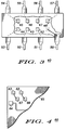
- FIG. 3 A specific example of an ESD sensor circuit 40 in accordance with the present invention, is illustrated in FIG. 3.
- Sensor circuit 40 is somewhat similar to sensor 30 of FIG. 2 in that a plurality of different individual sensors 42 through 48 are fabricated on a single substrate or support.
- Each sensor 42 through 48 includes a dielectric layer with a different thickness specifically selected and formed to withstand a different threshold voltage.
- a first or common contact is positioned adjacent the lower surface of each of the sensors 42 through 48 and a connection, which in this example is a wire bond, is made to an external pin 50.
- a plurality of second electrical contacts, one each positioned on each layer of the plurality of layers of dielectric material are formed to complete each sensor 42 through 48.
- An electrical connection (in this example a wire bond) is completed from the second electrical contact of each individual sensor 42 through 48 to a different external pin 51 through 57, respectively.
- each different thickness of each individual layer of the plurality of layers of dielectric material in sensors 42 through 48 is formed to provide a specific voltage at which an electrical short will occur between the first electrical contact 50 and the second electrical contact 51 through 57 positioned on the individual layer, so that sensor circuit 40 provides an indication of a range of voltages.
- sensor 42 has a threshold voltage of 50 volts
- sensor 43 has a threshold voltage of 100 volts
- sensor 44 has a threshold voltage of 200 volts
- sensor 45 has a threshold voltage of 300 volts
- sensor 46 has a threshold voltage of 500 volts
- sensor 47 has a threshold voltage of 1000 volts
- sensor 48 has a threshold voltage of 2000 volts.
- sensor circuit 40 is fabricated in a DIP package so that it can easily be incorporated into virtually any standard electrical circuit. Further, sensor circuit 40 can be included as a component in standard shipping packages, such as the well known plastic tubes, trays, etc. Thus, sensor circuit 40 is used to track components through assembly and shipping to determine any specific areas where ESD events are occurring. Once the position of the ESD events is determined a resolution to the problem can generally be relatively easily achieved.
- electrical circuit 60 can be an integrated circuit, a circuit formed on a printed circuit board, etc.
- Electrical circuit 60 includes a plurality of bonding pads 62, 63, and 64 positioned around the periphery of a substrate 65.
- electrical circuits have some additional unused bonding pads, which in this example are illustrated as bonding pads 62 and 63.
- bonding pads 62 and 63 are illustrated as bonding pads 62 and 63.
- a plurality of individual sensors 66 and 67 are formed on substrate 65 and one contact of each is connected to separate bonding pads 62 and 63, respectively.
- a common contact for sensors 66 and 67 is connected to a common contact for electrical circuit 60, such as ground.
- integrated or electrical circuit 60 includes a signal input, which may be for example bonding pad 64, having a known input capacitance.
- a signal input which may be for example bonding pad 64
- the layer of dielectric material and the second contact are formed with an area such that a capacitance formed therebetween is approximately the same size as the input capacitance of the signal input of the integrated circuit.
- bonding pads 62 and 63 will appear to an ESD event the same as input terminal 64 of the integrated circuit and the ESD event will have virtually the same effect on sensors 62 and 63 as it does on electrical circuit 60.
- ESD sensors and methods to monitor semiconductor components to determine when and/or how electrostatic discharges occurred is provided so that special precautions can be taken.
- ESD sensors can be made in wafer form so that ESD events can be tracked through a fabrication facility, all the way to saw or scribe stations.
- the ESD sensor can be provided in discrete form to monitor ESD events in packaging and shipping.
- ESD sensors can be added to most circuit boards and integrated circuits (early) to track major assembly operations. In all of these situations, if the ESD sensors remain as a permanent part of the system, they can be used to detect exposure to ESD events during system repair activities and other post fabrication activities.
- a new and improved ESD sensor is disclosed which is extremely small, inexpensive and simple to fabricate. Also, the new and improved ESD sensor and method of use provide a clear indication of an ESD event and is capable of indicating various characteristics of an ESD event, such as the size of the voltage as well as the exact time and date.
Landscapes
- Physics & Mathematics (AREA)
- General Physics & Mathematics (AREA)
- Electromagnetism (AREA)
- Elimination Of Static Electricity (AREA)
- Semiconductor Integrated Circuits (AREA)
- Light Receiving Elements (AREA)
- Solid State Image Pick-Up Elements (AREA)
Applications Claiming Priority (2)
| Application Number | Priority Date | Filing Date | Title |
|---|---|---|---|
| US634600 | 1984-07-26 | ||
| US08/634,600 US5796256A (en) | 1996-04-24 | 1996-04-24 | ESD sensor and method of use |
Publications (1)
| Publication Number | Publication Date |
|---|---|
| EP0803734A2 true EP0803734A2 (fr) | 1997-10-29 |
Family
ID=24544468
Family Applications (1)
| Application Number | Title | Priority Date | Filing Date |
|---|---|---|---|
| EP97106535A Withdrawn EP0803734A2 (fr) | 1996-04-24 | 1997-04-21 | Détecteur de décharge électrostatique et procédé d'utilisation |
Country Status (3)
| Country | Link |
|---|---|
| US (1) | US5796256A (fr) |
| EP (1) | EP0803734A2 (fr) |
| TW (1) | TW329557B (fr) |
Cited By (2)
| Publication number | Priority date | Publication date | Assignee | Title |
|---|---|---|---|---|
| CN103278708A (zh) * | 2013-04-25 | 2013-09-04 | 西安电子科技大学 | 一种基于低频噪声的esd监测设备 |
| US12416652B2 (en) | 2018-03-26 | 2025-09-16 | Analog Devices International Unlimited Company | Wearable device with energy harvesting |
Families Citing this family (14)
| Publication number | Priority date | Publication date | Assignee | Title |
|---|---|---|---|---|
| US5865361A (en) * | 1997-09-23 | 1999-02-02 | United States Surgical Corporation | Surgical stapling apparatus |
| US6660540B2 (en) * | 1999-04-09 | 2003-12-09 | Dupont Photomasks, Inc. | Test wafer and method for investigating electrostatic discharge induced wafer defects |
| US6368155B1 (en) * | 1999-07-16 | 2002-04-09 | Molex Incorporated | Intelligent sensing connectors |
| US6265885B1 (en) * | 1999-09-02 | 2001-07-24 | International Business Machines Corporation | Method, apparatus and computer program product for identifying electrostatic discharge damage to a thin film device |
| US7041365B2 (en) * | 2003-05-12 | 2006-05-09 | 3M Innovative Properties Company | Static dissipative optical construction |
| US7557725B2 (en) * | 2003-09-30 | 2009-07-07 | Intel Corporation | Event signature apparatus, systems, and methods |
| US7859279B2 (en) | 2006-11-01 | 2010-12-28 | Tokyo Electron Limited | Charge eliminating apparatus and method, and program storage medium |
| US7852325B2 (en) * | 2007-01-05 | 2010-12-14 | Apple Inc. | RF pulse synchronization for data acquisition operations |
| US8418046B2 (en) * | 2008-02-13 | 2013-04-09 | Apple Inc. | Data signal handling circuitry and methods with error analysis capabilities |
| US8264233B2 (en) * | 2009-07-29 | 2012-09-11 | Hitachi Global Storage Technologies, Netherlands B.V. | Magnetoresistive electrostatic discharge (ESD) detector |
| WO2013113766A1 (fr) | 2012-01-31 | 2013-08-08 | Micronic Mydata AB | Procédé de détection d'un risque d'endommagement de composants dans des ensembles électroniques |
| US9442597B2 (en) | 2012-10-19 | 2016-09-13 | Apple Inc. | Sensor-based ESD detection |
| US9811204B2 (en) | 2014-06-23 | 2017-11-07 | Apple Inc. | Time multiplexed touch detection and power charging |
| TWI858407B (zh) * | 2022-10-11 | 2024-10-11 | 強茂股份有限公司 | 可檢測靜電衝擊風險的封裝方法及封裝件 |
Family Cites Families (3)
| Publication number | Priority date | Publication date | Assignee | Title |
|---|---|---|---|---|
| JPH0769385B2 (ja) * | 1986-05-09 | 1995-07-31 | 沖電気工業株式会社 | 半導体装置の試験方法及びその装置 |
| US5359319A (en) * | 1990-08-13 | 1994-10-25 | Minnesota Mining And Manufacturing Company | Electrostatic discharge detector and display |
| US5376879A (en) * | 1992-11-03 | 1994-12-27 | Qrp, Incorporated | Method and apparatus for evaluating electrostatic discharge conditions |
-
1996
- 1996-04-24 US US08/634,600 patent/US5796256A/en not_active Expired - Fee Related
-
1997
- 1997-04-10 TW TW086104628A patent/TW329557B/zh active
- 1997-04-21 EP EP97106535A patent/EP0803734A2/fr not_active Withdrawn
Cited By (3)
| Publication number | Priority date | Publication date | Assignee | Title |
|---|---|---|---|---|
| CN103278708A (zh) * | 2013-04-25 | 2013-09-04 | 西安电子科技大学 | 一种基于低频噪声的esd监测设备 |
| CN103278708B (zh) * | 2013-04-25 | 2016-01-20 | 西安电子科技大学 | 一种基于低频噪声的esd监测设备 |
| US12416652B2 (en) | 2018-03-26 | 2025-09-16 | Analog Devices International Unlimited Company | Wearable device with energy harvesting |
Also Published As
| Publication number | Publication date |
|---|---|
| TW329557B (en) | 1998-04-11 |
| US5796256A (en) | 1998-08-18 |
Similar Documents
| Publication | Publication Date | Title |
|---|---|---|
| US5796256A (en) | ESD sensor and method of use | |
| US7224949B2 (en) | ESD protection circuit for radio frequency input/output terminals in an integrated circuit | |
| EP0788161A2 (fr) | Dispositif microélectronique avec une structure de protection à film mince contre des décharges électrostatiques | |
| US5276582A (en) | ESD protection using npn bipolar transistor | |
| US7205613B2 (en) | Insulating substrate for IC packages having integral ESD protection | |
| US4617605A (en) | Carrier element for an IC module | |
| EP2295992B1 (fr) | Dispositif pour détecter et mesurer la charge de l'électricité statique | |
| EP1750309A2 (fr) | Dispositif émetteur de lumière à élément de protection | |
| US10147688B2 (en) | Integrated circuit device with overvoltage discharge protection | |
| US20030235019A1 (en) | Electrostatic discharge protection scheme for flip-chip packaged integrated circuits | |
| US6714392B2 (en) | Electronic component and utilization of a guard structure contained therein | |
| JPS63151063A (ja) | 静電的放電からの集積回路の保護方法及び保護構造 | |
| WO1998044607A1 (fr) | Configuration de protection contre les decharges electrostatiques dans les appareils electroniques | |
| US6876529B2 (en) | Electrostatic discharge protection circuit | |
| EP0109070B1 (fr) | Dispositif semi-conducteur du type MOS | |
| US8753960B1 (en) | Integrated circuit devices with electrostatic discharge (ESD) protection in scribe line regions | |
| US4942495A (en) | Electrostatic protection device for electronic cards | |
| US6364731B1 (en) | Circuit device manufacturing equipment | |
| US6667860B1 (en) | Integrated, on-board device and method for the protection of magnetoresistive heads from electrostatic discharge | |
| US6143586A (en) | Electrostatic protected substrate | |
| US12148748B2 (en) | On-chip electrostatic discharge sensor | |
| KR100206047B1 (ko) | 고체상태 기구용 정전기 방전 전압 보호 회로 | |
| US5411896A (en) | Method of making supra-passivant grid | |
| US5976901A (en) | Process for manufacturing semiconductor devices with active structures | |
| JPS5951558A (ja) | 半導体装置 |
Legal Events
| Date | Code | Title | Description |
|---|---|---|---|
| PUAI | Public reference made under article 153(3) epc to a published international application that has entered the european phase |
Free format text: ORIGINAL CODE: 0009012 |
|
| AK | Designated contracting states |
Kind code of ref document: A2 Designated state(s): DE FR GB |
|
| STAA | Information on the status of an ep patent application or granted ep patent |
Free format text: STATUS: THE APPLICATION HAS BEEN WITHDRAWN |
|
| 18W | Application withdrawn |
Withdrawal date: 19981207 |