EP0803136B1 - Printed circuit board connectors - Google Patents
Printed circuit board connectors Download PDFInfo
- Publication number
- EP0803136B1 EP0803136B1 EP95944472A EP95944472A EP0803136B1 EP 0803136 B1 EP0803136 B1 EP 0803136B1 EP 95944472 A EP95944472 A EP 95944472A EP 95944472 A EP95944472 A EP 95944472A EP 0803136 B1 EP0803136 B1 EP 0803136B1
- Authority
- EP
- European Patent Office
- Prior art keywords
- contact
- line
- attached
- subassemblies
- face
- Prior art date
- Legal status (The legal status is an assumption and is not a legal conclusion. Google has not performed a legal analysis and makes no representation as to the accuracy of the status listed.)
- Expired - Lifetime
Links
- 238000002347 injection Methods 0.000 claims description 5
- 239000007924 injection Substances 0.000 claims description 5
- 238000005476 soldering Methods 0.000 claims description 2
- 125000006850 spacer group Chemical group 0.000 description 17
- 230000013011 mating Effects 0.000 description 6
- 229910052782 aluminium Inorganic materials 0.000 description 4
- MTCPZNVSDFCBBE-UHFFFAOYSA-N 1,3,5-trichloro-2-(2,6-dichlorophenyl)benzene Chemical compound ClC1=CC(Cl)=CC(Cl)=C1C1=C(Cl)C=CC=C1Cl MTCPZNVSDFCBBE-UHFFFAOYSA-N 0.000 description 3
- 230000000284 resting effect Effects 0.000 description 3
- XAGFODPZIPBFFR-UHFFFAOYSA-N aluminium Chemical compound [Al] XAGFODPZIPBFFR-UHFFFAOYSA-N 0.000 description 2
- 239000004020 conductor Substances 0.000 description 2
- 238000001125 extrusion Methods 0.000 description 2
- 229910052751 metal Inorganic materials 0.000 description 2
- 239000002184 metal Substances 0.000 description 2
- 239000011248 coating agent Substances 0.000 description 1
- 238000000576 coating method Methods 0.000 description 1
- 230000006835 compression Effects 0.000 description 1
- 238000007906 compression Methods 0.000 description 1
- 238000002788 crimping Methods 0.000 description 1
- 230000003467 diminishing effect Effects 0.000 description 1
- 238000001746 injection moulding Methods 0.000 description 1
- 238000004519 manufacturing process Methods 0.000 description 1
- 238000002156 mixing Methods 0.000 description 1
- 230000004048 modification Effects 0.000 description 1
- 238000012986 modification Methods 0.000 description 1
- 239000002243 precursor Substances 0.000 description 1
- 229910001220 stainless steel Inorganic materials 0.000 description 1
- 239000010935 stainless steel Substances 0.000 description 1
- 238000004804 winding Methods 0.000 description 1
Images


Classifications
-
- H—ELECTRICITY
- H01—ELECTRIC ELEMENTS
- H01R—ELECTRICALLY-CONDUCTIVE CONNECTIONS; STRUCTURAL ASSOCIATIONS OF A PLURALITY OF MUTUALLY-INSULATED ELECTRICAL CONNECTING ELEMENTS; COUPLING DEVICES; CURRENT COLLECTORS
- H01R12/00—Structural associations of a plurality of mutually-insulated electrical connecting elements, specially adapted for printed circuits, e.g. printed circuit boards [PCB], flat or ribbon cables, or like generally planar structures, e.g. terminal strips, terminal blocks; Coupling devices specially adapted for printed circuits, flat or ribbon cables, or like generally planar structures; Terminals specially adapted for contact with, or insertion into, printed circuits, flat or ribbon cables, or like generally planar structures
- H01R12/70—Coupling devices
- H01R12/7082—Coupling device supported only by cooperation with PCB
-
- H—ELECTRICITY
- H01—ELECTRIC ELEMENTS
- H01R—ELECTRICALLY-CONDUCTIVE CONNECTIONS; STRUCTURAL ASSOCIATIONS OF A PLURALITY OF MUTUALLY-INSULATED ELECTRICAL CONNECTING ELEMENTS; COUPLING DEVICES; CURRENT COLLECTORS
- H01R12/00—Structural associations of a plurality of mutually-insulated electrical connecting elements, specially adapted for printed circuits, e.g. printed circuit boards [PCB], flat or ribbon cables, or like generally planar structures, e.g. terminal strips, terminal blocks; Coupling devices specially adapted for printed circuits, flat or ribbon cables, or like generally planar structures; Terminals specially adapted for contact with, or insertion into, printed circuits, flat or ribbon cables, or like generally planar structures
- H01R12/70—Coupling devices
- H01R12/71—Coupling devices for rigid printing circuits or like structures
- H01R12/712—Coupling devices for rigid printing circuits or like structures co-operating with the surface of the printed circuit or with a coupling device exclusively provided on the surface of the printed circuit
- H01R12/716—Coupling device provided on the PCB
-
- H—ELECTRICITY
- H01—ELECTRIC ELEMENTS
- H01R—ELECTRICALLY-CONDUCTIVE CONNECTIONS; STRUCTURAL ASSOCIATIONS OF A PLURALITY OF MUTUALLY-INSULATED ELECTRICAL CONNECTING ELEMENTS; COUPLING DEVICES; CURRENT COLLECTORS
- H01R12/00—Structural associations of a plurality of mutually-insulated electrical connecting elements, specially adapted for printed circuits, e.g. printed circuit boards [PCB], flat or ribbon cables, or like generally planar structures, e.g. terminal strips, terminal blocks; Coupling devices specially adapted for printed circuits, flat or ribbon cables, or like generally planar structures; Terminals specially adapted for contact with, or insertion into, printed circuits, flat or ribbon cables, or like generally planar structures
- H01R12/70—Coupling devices
- H01R12/71—Coupling devices for rigid printing circuits or like structures
- H01R12/72—Coupling devices for rigid printing circuits or like structures coupling with the edge of the rigid printed circuits or like structures
- H01R12/721—Coupling devices for rigid printing circuits or like structures coupling with the edge of the rigid printed circuits or like structures cooperating directly with the edge of the rigid printed circuits
-
- Y—GENERAL TAGGING OF NEW TECHNOLOGICAL DEVELOPMENTS; GENERAL TAGGING OF CROSS-SECTIONAL TECHNOLOGIES SPANNING OVER SEVERAL SECTIONS OF THE IPC; TECHNICAL SUBJECTS COVERED BY FORMER USPC CROSS-REFERENCE ART COLLECTIONS [XRACs] AND DIGESTS
- Y10—TECHNICAL SUBJECTS COVERED BY FORMER USPC
- Y10S—TECHNICAL SUBJECTS COVERED BY FORMER USPC CROSS-REFERENCE ART COLLECTIONS [XRACs] AND DIGESTS
- Y10S439/00—Electrical connectors
- Y10S439/947—PCB mounted connector with ground terminal
Definitions
- This invention relates to connectors for printed circuit boards (“PCB”s), and more particularly to such connectors which include pressure mounted contacts.
- Printed circuit board connectors are known in which two relatively movable insulating housings carry as contact elements respectively conductor pads (or “blades”) and conductor cantilever beams carrying pressure mounted surfaces, mounted on the housings for wiping engagement of contact surfaces of the pads and beams as the connectors are moved in a connector-mating direction.
- a PCB connector element may desirably be provided with a plurality of sets of contact elements secured in a housing with contact surfaces of the contact elements facing away from the housing.
- the sets are arranged in rows spaced transversely of the housing, one set is of leaf spring cantilever beam contact elements with one end held in the housing, and the other set is surface mounted on the housing, with its ends held in the housing, contact elements of one set alternating longitudinally of the housing with contact elements of the other set.
- a PCB connector element may desirably be provided with a pressure-mounted contact element, the contact element being a leaf spring cantilever beam with one end held in a housing, the beam being stressed into strain by abutment in the housing limiting movement of the other end.
- the beam portion between the held end and a contact surface portion has a cross-sectional area diminishing in the direction from the fixedly mounted end toward the contact portion, and the contact surface portion extends away from the housing through a hole therein.
- a PCB connector may be provided which includes two connector elements mounted in relation to each other such as to matingly engage another PCB connector also having two connector elements, connector elements of one PCB connector including daughter board leads arranged to engage daughter board surface mounted contacts to provide a daughter board connector and connector elements of the other PCB connector including backplane leads adapted to engage backplane surface mounted contacts, to provide a backplane connector.
- the backplane connector has a central spine on which transversely opposed connector elements are carried and the daughter board connector has transversely spaced pairs of connector elements mounted on spacers corresponding in thickness functionally to the overall thickness of the backplane connector.
- a PCB connector element may be desirably supplied in the form of a longitudinally extending support carrying a pair of transversely spaced housings each carrying transversely accessible contact surfaces.
- one such connector element is transversely spaced by a spine on which housings are mounted and the other such connector element has housings held in spaced relation by spacers, the spacers having longitudinal edge ribs slidably fitting in tracks of mounting ribs, and the spined connector element being matably engageable with the spacer connector element, whereby on mating contact surfaces of the spine connector element wipingly engage contact surfaces of the spacer connector.
- the invention relates to an electrical connector as defined in claim 1 and as defined in claim 7.
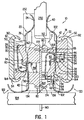
- Fig. I is an enlarged sectional view of the preferred embodiment, taken at 1-1 of Figures 6 and 8.
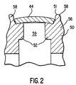
- Fig. 2 is a broken-away sectional view taken at 2-2 of Fig. 4.
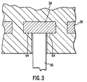
- Fig. 3 is a broken-away sectional view taken at 3-3 of Fig. 1.
- Fig. 4 is a front elevation, partially diagrammatic, of a subassembly of the preferred embodiment.
- Fig. 5 is a rear elevation, broken away and to a larger scale, of the subassembly of Fig. 4.
- Fig. 6 is a broken-away plan view of the backplane connector of said embodiment.
- Fig. 7 is a corresponding side elevation view of said backplane connector, with some details omitted, mounted on a printed circuit board.
- Fig. 8 is a corresponding plan view of the spine element of a modified embodiment.
- Fig. 9 is a corresponding side elevation view of said spine element.
- Fig. 10 is a side elevational broken-away view of a web adapted for winding on a reel, showing two beam contact elements of the invention.
- Fig. 11 is an isometric, partial, partially exploded view of a daughter-board-supporting spacer and the rails carried by it.
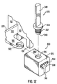
- Fig. 12 is an exploded isometric view, partially broken away, of a backplane spine of the preferred embodiment carrying a pair of housings and arranged to accept a D-pin carrying block.
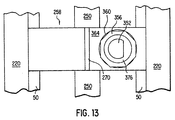
- Fig. 13 is a bottom view, broken away and partially diagrammatic, of the daughter board connector of said preferred embodiment.
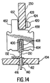
- Fig. 14 is a sectional view taken at 14-14 of Fig. 9.
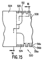
- Fig. 15 is a partial plan view of a fixture for assembling the daughter board connector of the preferred embodiment.
- Fig. 16 is a sectional view taken at 16-16 of Fig. 15.
- a connector assembly (indicated generally at 10 in Fig. 1) includes a backplane connector indicated generally at 12 and a daughter board connector indicated generally at 14.
- Backplane connector 12 and daughterboard connector 14 each includes a multiplicity of contact elements 20 and 22, one of each of which is shown in Fig. 1.
- each of the housings 50 of each connector 12, 14 there are in each of the housings 50 of each connector 12, 14 one fewer of the contact elements 22 than of the contact elements 20.
- the housings 50 are reversely transversely (vertically, in the figure) oriented.
- the housings 50 are longitudinally offset in both connectors 12 and 14.
- the parts are arranged (holes, tabs, dimensions) so that this offset is by an amount equal to half the centerline distances between holes 68 and between pads 44 (both of which are on identical centerline spacings), with centerlines of holes 68 and pads 44 arranged to occur alternately, as shown in Fig. 4.
- Fig. 1 could be a vertical section in a single plane, rather than a section jogged into two planes as drawn in Figs. 3, 6.
- Each contact element 20 includes a daughter board contact portion 24, a lead portion 26, a support portion 28, a beam portion 30, a generally elliptical out-of-round arcuate contact contact portion 32 describing about certain points a circumference encompassing more than 180 degrees, and a second support portion 34 oriented about 90 degrees relative to the first support portion 28.
- Each contact element 22 includes a daughter board contact portion 40, a lead portion 42, a pad portion 44 and an end 46.
- End 46 and lead 42 are anchored in housing 50 (through their position, during injection molding of the housing), and pad 44 is supported by transverse support ribs 52 also injection molded as part of housing 50 and extending over the back of pad 44, generally longitudinally centrally of pad 44, partially inwardly transversely thereof on each rear side thereof.
- Ribs 52 are injection molded integrally with longitudinal ribs 54, which are integral with plastic portions 56 into which pad ends 46 are anchored.
- ribs 58 molded integrally with plastic portions 56 and the rest of housing 50. Ribs 58 provide outer transversely curved surfaces 57 (Fig.
- a subassembly 100 shown in Fig. 4 can be better seen beam contact holes 68, pads 44, and ribs 58 of housing 50. Also shown are legs 102, for resting on a backplane 104 when part of a backplane connector 12, or sticking harmlessly in mid air when part of a daughter board connector 14 (Fig. 1).
- Backplane connector 12 has a contact element indicated generally at 122 and which is identical with contact element 22 except that it is bent at a greater angle between portion 42 and its PCB (here backplane) contact portion 122.
- the other contact element of backplane connector 12, which is indicated generally at 120, is identical with contact element 20, except that it is bent at a greater angle to portion 26 to provide the backplane contact portion indicated generally at 120.
- Housings 50 are supported, and longitudinally located relative to each other, on tabs 80, struck out from metal spine 130, as shown in more detail in Figs. 8 and 9.
- Figs. 8 and 9 illustrate the spine of a modification, with tabs 80 entering not only upper portions of housing 50 as in Fig. 1, but corresponding lower portions as well, the lower tabs being substituted for the grips 82 shown in Fig. 1; in the Fig. 1 embodiment the lower tabs of Fig. 1 extend outwardly to a greater distance from the spine, as would be better seen in a figure corresponding with Fig. 8, and have a configuration as would be seen in such a figure with flat longitudinally spaced edges having a transversely convex edge therebetween.)
- the spine includes also flange 132 to cooperate in mounting the spine on backplane 104, on which the spine 130 rests on coplanar edge 133 as well.
- Spine 130 also includes at each end (one not shown, but extending from the spine in the same transverse direction as the other, shown) an end support flange 134, with a lower surface like the lower surfaces of edge 133 and flange 132 coplanar and resting on backplane 104. Finally is middle support flange 136, struck out from spine 130 like the others, and with lower surface coplanar with theirs and resting on PCB 104 but extending transversely oppositely to flanges 132 and 134 to spine 130.
- dynamic contact pins 140 integral with the spine, for making compression contact through their elongated slot portions with conductive holes in PCB 104.
- guide post 148 Mounted in hole 144 of flange 136 (Figs. 6 and 7), and coaxial hole (not shown) in PCB 104 is guide post 148.
- FIGs. 6 and 7 There are shown in Figs. 6 and 7 two and a fraction sets of housings 50 of backplane connector 12.
- Ridges 162 and 164 are in cross-section half a semicircle on their non-mating (away from contact surfaces of contact elements) sides; and on their other sides at 45 degrees to the plane of nearby surfaces (Fig. 5) 172 (longitudinally continuous) and 174 (longitudinally discontinuous), blending into an extension of the half semicircle already mentioned into three-quarters of a semicircle, or about 135 degrees.
- the ridges are relieved angling upwardly, as seen for ridge 162 in Figs. 4 and 5; as seen in Figs. 6 and 7, each housing 50 includes two ridges 162 and (not there shown) two ridges 164.
- Relief at the end of each ridge 162 and 164 is by planes through the back halves of the ridges at angles of 90 degrees to both the faces 172, 174 and 45 degrees to the ends of the housings, and through the front halves of the ridges by planes at 45 degrees to the faces 172, 174 and to the ends of the housings as well.
- the relieved portions at the ends of ridges 162, 164 are for crimping thereinto the inwardly extending upper and lower portions of tracks 220, to further secure relative thereto housings 50.
- Extending into the backs, or non-mating, sides (Fig. 5) of housing 50 are rectangular blind holes 168 extending from surfaces 172 partially through housing 50. Hole locations 168 are longitudinally spaced as are upper tabs 80 in the embodiment of Fig. 1, lower tabs 80 of Fig. 8 being replaced by the different tabs 82 as shown in Fig. 1 and already explained. As shown in Fig. 1, tabs or grips 82 are crimped around ridges 164 (after inserting tabs 80 and moving housing 50 into position).
- each rib including a narrow outer surface 184 coplanar with surface 172. From each of the two edges of surface 184 extend a pair of guide surfaces 188 widening therebetween in a 45 degree chamfer.
- Beneath pads 44 are narrow ribs 192 integrally injection molded with the rest of housing 50 separating beam portions 30 of contact elements 20 and 120. Integral with narrow ribs 192 are wide ribs indicated generally at 196 with central flat surfaces 202 coplanar with the outer surface of narrow ribs 192, and with 45 degree chamfer 206. Between the ribs 196 extend contact element portions 26 (Fig. 1).
- housing portion 210 Above the wide ribs 196 in this view is housing portion 210.
- Daughter board connector 14 includes opposed housings 50 incorporating contact elements as seen identical in form (except for the angle of bend of their daughter board contact portions, already mentioned) and arrangement with the housing subassemblies in backplane connector 12.
- the contact element portions 24, 40 and 42, 26 are soldered on soldered surface mounting pads carried in a way conventional in the art on, respectively, daughter board 250 and backplane 104.
- Fig. 10 is seen a pair of shepherd's crook beam contact element 20, 120 precursors, while still integral through ribs 230, 234 with drive wheel contact portion 238, through which extend drive wheel pin receiving holes 242.
- the blanks for what will become pad contact elements 22, 122 are also prepared in reels to facilitate handling.
- Daughter boards 250 are held (against ear 252 surface 248) by screws (not shown) extending into threaded (not shown) holes 254 in extruded aluminum spacers indicated generally at 258 (Fig. 11) including ridges 262, 264 shaped and spaced just as are ridges 162, 164 for alignment therealong in the holding tracks 220. Also extruded into spacer 258 is groove 270, extending down to just above the top surface 272 of spine 130, for accepting spine 130 in notch 400, to align spacer 258.
- a spacer 258 is provided along tracks 220 between each longitudinally adjoining pair of housings 50, as well as outboard of each outermost such pair; in the preferred embodiment are four pairs of such housings and thus five spacers 258.
- each of tabs 132 Mounted on each of tabs 132, one on each side of tab 136 and both extending transversely of spine 130 in the same transverse direction, are (Fig. 12) extruded aluminum key blocks indicated generally at 300, through which in a transverse direction extend a wide slot 304, a narrower notch 308 opening thereinto, and a slot 312 opening into notch 308.
- a D-pin 348 fits locatingly into a D-hole 352 (Fig. 13) extending upwardly into sintered stainless steel octagonal insert 356 force fitted into counterbore 360 to bottom thereon in spacer 258 at about a third of the spacer height above bottom surface 364, the counterbore 360 and hole 362 (Fig. 11) coaxial centerline being halfway between the two flat surfaces 368 and halfway between notch 270 and the ridges 262, 264 farther from ear 252 and extending parallel to all four surfaces 368, 372.
- Octagonal insert 356 includes pin guide countersink 376 and may be with D-pin 348 rotationally oriented as desired to affect pin mating.
- Bottom surface 364 of spacer 258 engages top surface 380 of key block 300 in each instance, to provide important locating orientation among the parts of the overall assembly.
- Post or guide pin 148 (Figs. 6, 7) at its upper end is : accepted by hole 362 in spacer 258, to index backplane 104 to daughter board 250.
- the beam contact members 20, 120 are supplied to customers still connected by the bar 230 (Fig. 10); after soldering 24 or 120 to a PCB pad, they may then break off leads 24, for example, at score lines (not shown) conveniently placed just outboard of where they are soldered to the board pads.
- housing 50 longitudinally 71.5, and transversely, centrally, 3.4
- track 220 transversely, outside 12.93 by 3.7
- block 300 slot 304 longitudinally of spine, 3.5 and slot 312 (in the same direction) 1.2
- leads 24, beams 30, and pads 58 are each on 1.0 centerlines.
- the leads extending from the top in Fig. 1 could be shaped like the leads extending from the bottom, whereupon a connector assembly for stacked PCB's would result. Or those at the bottom could be shaped like those at the top, to connect boards in line rather than either perpendicular or parallel.
- Each contact element could include a beam contact portion to contact that of the other; one contact portion surface might have its contact surface cylindrically concave to engage a convex cylindrical surface of the other.
- the single row of tabs 80 left remaining in Fig. 1 could be replaced with a second row of jaws 82 cooperating with mating notches in at least one of the ridges 162, 164 in order for relative longitudinal location as well as holding of the housings.
- FIG. 14 A further important embodiment is shown in Fig. 14.
- Female contact 404 is press-fitted in enlarged slot 408 of spacer 458, otherwise like spacer 258.
- Plated through hole 412 of backplane 104 provides the usual spool-shaped conductive coating element 416.
- Head 420 of a screw extending through daughter board 250 and into a threaded hole in ear 452 (which is identical with ear 252) rests on metal washer 424, which engages in turn lip 428 of a plated through conductive spool like 416, the other lip or flange of which is shown at 432.
- FIG. 15 and 16 A fixture useful in assembly of daughter boards according to the preferred embodiment is shown in Figs. 15 and 16.
- a bar indicated generally at 500 Illustrated is part of one spacer 258 accepting notch 504 and one subassembly accepting portion 508.
- the bar includes four portions 508 and five portions 504, with a portion not shown and like portions 508 except shorter and without grooves 512.
- Grooves 512 are defined by rectilinear ribs 516, which include stepped portions 516a, 516b, and 516c.
- Recesses 520, 524 allow for acceptance of housing legs 102.
- Housings are fitted on jig 500 with ribs 58 in grooves 512 and ribs 516 toward pads 44. Once positional relationships are set, tracks 220 are crimped to fix these relationships. Bar 500 may then be removed downwardly.
Landscapes
- Coupling Device And Connection With Printed Circuit (AREA)
- Details Of Connecting Devices For Male And Female Coupling (AREA)
Abstract
Description
Claims (10)
- An electrical connector comprising a plurality of first subassemblies and a plurality of second subassemblies, each first subassembly (100) and each second subassembly (100) including an insulating housing (50) and a plurality of contact elements (20, 22, 120, 122) disposed in the insulating housing, the plurality of contact elements of each first subassembly engaging the plurality of contact elements of a corresponding second subassembly, characterized in that:the respective insulating housings of the plurality of first subassemblies and the plurality of second subassemblies are identical,a portion of the plurality of first subassemblies is attached to a first surface of a first support member (130),a portion of the plurality of second subassemblies is attached to a surface of a second support member (220),each contact element has a contact portion (44, 66) disposed on a face (172) of a corresponding insulating housing (50), andthe contact portions disposed on the face of the corresponding insulating housing are arranged in a first line and in a second line, wherein the contact portions in the first line and the contact portions in the second line are longitudinally offset, whereby the centerlines of the contact portions in the first line are between the centerlines of the contact portions in the second line.
- The electrical connector of claim 1wherein the contact portions (66) in the first line are shaped like beams and the contact portions (44) in the second line are shaped like pads.
- The electrical connector of claim 2wherein the face of each insulating housing has a plurality of holes (68) therethrough, the holes being disposed along the first line,wherein the contact portions shaped like beams project through adjacent holes, andwherein the number of holes is greater than the number of contact portions shaped like beams,whereby the first subassemblies attached to the first support member have an empty hole at an end of the first line, and the second subassemblies attached to the second support member have an empty hole at an opposite end of the first line.
- The electrical connector of claim 1wherein the first support member has a second surface parallel to the first surface, andwherein another portion of the plurality of first subassemblies is attached to the second surface,whereby the faces of the insulating housings attached to the first surface and the faces of the insulating housings attached to the second surface point in opposite directions.
- The electrical connector of claim 4further comprising a third support member (220) joined to the second support member,wherein another portion of the plurality of second subassemblies is attached to the third support member, andwherein the first subassemblies attached to the first support member are disposed between the second subassemblies attached to the second support member and the second subassemblies attached to the third support member.
- The electrical connector of claim 5wherein the contact portions (66) in the first line are shaped like beams, and the contact portions (44) in the second line are shaped like pads,wherein the contact portions shaped like beams and disposed on the face of each insulating housing attached to the first support member engage the contact portions shaped like pads and disposed on the face of corresponding insulating housings attached to the second and third support members, andwherein the contact portions shaped like pads and disposed on the face of each insulating housing attached to the first support member engage the contact portions shaped like beams and disposed on the face of corresponding insulating housings attached to the second and third support members.
- An electrical connector comprising:a) an insulating housing (50) having a face (172);b) a plurality of first contact elements (20, 120) extending through the face, each first contact element including a beam (66), the beams being disposed along a first line across the face; andc) a plurality of second contact elements (22, 122), each second contact element including a contact pad (44), the contact pads being disposed along a second line across the face,wherein the first line and the second line are substantially parallel to each other, andwherein the beams disposed along the first line and the contact pads disposed along the second line are longitudinally offset, whereby the centerlines of the beams are between the centerlines of the pads.
- The electrical connector of claim 7wherein the insulating housing further comprises a plurality of ribs (52) disposed on the face between adjacent contact pads, andwherein the plurality of second contact elements is injection molded within the housing.
- The electrical connector of claim 7wherein the face includes a plurality of openings (68) therethrough, disposed along the first line,wherein each beam projects through one of the plurality of openings, andwherein the number of openings is greater than the number of beams.
- The electrical connector of claim 7wherein each first contact element and each second contact element further includes a contact (24, 40, 42, 26) for soldering to a printed circuit board.
Applications Claiming Priority (3)
| Application Number | Priority Date | Filing Date | Title |
|---|---|---|---|
| US372494 | 1995-01-13 | ||
| US08/372,494 US5595490A (en) | 1995-01-13 | 1995-01-13 | Printed circuit board connectors |
| PCT/US1995/015711 WO1996021956A1 (en) | 1995-01-13 | 1995-12-04 | Printed circuit board connectors |
Publications (2)
| Publication Number | Publication Date |
|---|---|
| EP0803136A1 EP0803136A1 (en) | 1997-10-29 |
| EP0803136B1 true EP0803136B1 (en) | 1999-07-21 |
Family
ID=23468365
Family Applications (1)
| Application Number | Title | Priority Date | Filing Date |
|---|---|---|---|
| EP95944472A Expired - Lifetime EP0803136B1 (en) | 1995-01-13 | 1995-12-04 | Printed circuit board connectors |
Country Status (7)
| Country | Link |
|---|---|
| US (1) | US5595490A (en) |
| EP (1) | EP0803136B1 (en) |
| JP (1) | JPH10512389A (en) |
| AT (1) | ATE182424T1 (en) |
| CA (1) | CA2208834A1 (en) |
| DE (1) | DE69510956T2 (en) |
| WO (1) | WO1996021956A1 (en) |
Families Citing this family (10)
| Publication number | Priority date | Publication date | Assignee | Title |
|---|---|---|---|---|
| US6036504A (en) * | 1996-12-27 | 2000-03-14 | Hon Hai Precision Ind. Co., Ltd. | Board-to-board connector assembly |
| US6231391B1 (en) | 1999-08-12 | 2001-05-15 | Robinson Nugent, Inc. | Connector apparatus |
| ATE526706T1 (en) * | 1998-08-12 | 2011-10-15 | 3M Innovative Properties Co | CONNECTOR DEVICE |
| US6187246B1 (en) | 1998-12-31 | 2001-02-13 | Berg Technology, Inc. | Method of manufacturing an extended height insulative housing for an electrical connector |
| US6625881B2 (en) | 2001-09-11 | 2003-09-30 | Xytrans, Inc. | Solderless method for transferring high frequency, radio frequency signals between printed circuit boards |
| US6905367B2 (en) | 2002-07-16 | 2005-06-14 | Silicon Bandwidth, Inc. | Modular coaxial electrical interconnect system having a modular frame and electrically shielded signal paths and a method of making the same |
| US7484971B2 (en) | 2005-11-29 | 2009-02-03 | Amphenol Corporation | Electronic component with high density, low cost attachment |
| US7630210B2 (en) * | 2005-11-29 | 2009-12-08 | Amphenol Corporation | Lead(Pb)-free electronic component attachment |
| US20090163047A1 (en) * | 2007-12-24 | 2009-06-25 | Myoungsoo Jeon | Connector having both press-fit pins and high-speed conductive resilient surface contact elements |
| US7544067B1 (en) * | 2008-02-29 | 2009-06-09 | Tyco Electronics Amp K.K. | Board mount-type connector and board mount-type connector assembly |
Family Cites Families (10)
| Publication number | Priority date | Publication date | Assignee | Title |
|---|---|---|---|---|
| FR1604372A (en) * | 1968-10-01 | 1971-11-08 | ||
| SU752551A1 (en) * | 1978-01-09 | 1980-07-30 | Организация П/Я Х-5263 | Electric contact apparatus for ageing and testing baseless electric discharge devices |
| EP0125780A1 (en) * | 1983-04-13 | 1984-11-21 | AMP INCORPORATED (a New Jersey corporation) | Surface mountable expansion matching connector |
| GB2225492A (en) * | 1988-10-14 | 1990-05-30 | Itt Ind Ltd | Electrical connector for PCB |
| US4863395A (en) * | 1989-01-17 | 1989-09-05 | Robert Babuka | Zero insertion force connector with component card |
| US4973270A (en) * | 1989-06-02 | 1990-11-27 | Amp Incorporated | Circuit panel socket with cloverleaf contact |
| US5161985A (en) * | 1991-08-08 | 1992-11-10 | Robinson Nugent, Inc. | Board to board interconnect |
| US5171154A (en) * | 1991-11-06 | 1992-12-15 | Amp Incorporated | High density backplane connector |
| US5310357A (en) * | 1993-02-22 | 1994-05-10 | Berg Technology, Inc. | Blade-like terminal having a passive latch |
| JP2598650Y2 (en) * | 1993-12-14 | 1999-08-16 | モレックス インコーポレーテッド | Electrical connector for connecting printed circuit boards |
-
1995
- 1995-01-13 US US08/372,494 patent/US5595490A/en not_active Expired - Lifetime
- 1995-12-04 WO PCT/US1995/015711 patent/WO1996021956A1/en not_active Ceased
- 1995-12-04 EP EP95944472A patent/EP0803136B1/en not_active Expired - Lifetime
- 1995-12-04 JP JP8521651A patent/JPH10512389A/en active Pending
- 1995-12-04 DE DE69510956T patent/DE69510956T2/en not_active Expired - Fee Related
- 1995-12-04 CA CA002208834A patent/CA2208834A1/en not_active Abandoned
- 1995-12-04 AT AT95944472T patent/ATE182424T1/en not_active IP Right Cessation
Also Published As
| Publication number | Publication date |
|---|---|
| EP0803136A1 (en) | 1997-10-29 |
| DE69510956T2 (en) | 1999-12-23 |
| JPH10512389A (en) | 1998-11-24 |
| DE69510956D1 (en) | 1999-08-26 |
| US5595490A (en) | 1997-01-21 |
| WO1996021956A1 (en) | 1996-07-18 |
| CA2208834A1 (en) | 1996-07-18 |
| ATE182424T1 (en) | 1999-08-15 |
Similar Documents
| Publication | Publication Date | Title |
|---|---|---|
| US4607907A (en) | Electrical connector requiring low mating force | |
| US7806698B2 (en) | Edge card connector assembly with high-speed terminals | |
| US9871323B2 (en) | Electrical connector with reduced stack height | |
| EP0233914B1 (en) | Surface mount connector | |
| US4818237A (en) | Modular plug-in connection means for flexible power supply of electronic apparatus | |
| US10784630B1 (en) | Female connector and transmission wafer | |
| US5145386A (en) | Low profile electrical connector | |
| EP0803136B1 (en) | Printed circuit board connectors | |
| US7727001B2 (en) | Electrical connector assembly | |
| US4660917A (en) | Multi-wire insulation displacement terminal | |
| CN101432932A (en) | Electrical connector assembly with selective arrangement of signal and ground contacts | |
| JPS5854474B2 (en) | Connector assembly for leadless integrated circuit package | |
| EP0555368B1 (en) | Electrical connectors having tapered spring contact element | |
| US4795374A (en) | Double sided edge connector | |
| DE69305544T2 (en) | Extension socket for readout boards equipped on both sides | |
| JPS61253777A (en) | Electric jumper | |
| US5470246A (en) | Low profile edge connector | |
| US5256073A (en) | Electrical connectors for direct connection to plated through holes in circuit board | |
| US6000955A (en) | Multiple terminal edge connector | |
| EP0529345A2 (en) | Card edge connector assembly | |
| US20060135003A1 (en) | Connector with improved dual beam contacts | |
| JP2683706B2 (en) | Electrical connector | |
| EP0364104B1 (en) | Miniature barrel female terminal | |
| WO1990007806A1 (en) | Electrical connector | |
| CN1096126C (en) | Electrical connector with integral supporting structure |
Legal Events
| Date | Code | Title | Description |
|---|---|---|---|
| PUAI | Public reference made under article 153(3) epc to a published international application that has entered the european phase |
Free format text: ORIGINAL CODE: 0009012 |
|
| 17P | Request for examination filed |
Effective date: 19970721 |
|
| AK | Designated contracting states |
Kind code of ref document: A1 Designated state(s): AT BE CH DE DK FR GB IE IT LI LU MC NL PT SE |
|
| 17Q | First examination report despatched |
Effective date: 19971107 |
|
| GRAG | Despatch of communication of intention to grant |
Free format text: ORIGINAL CODE: EPIDOS AGRA |
|
| GRAG | Despatch of communication of intention to grant |
Free format text: ORIGINAL CODE: EPIDOS AGRA |
|
| GRAH | Despatch of communication of intention to grant a patent |
Free format text: ORIGINAL CODE: EPIDOS IGRA |
|
| GRAH | Despatch of communication of intention to grant a patent |
Free format text: ORIGINAL CODE: EPIDOS IGRA |
|
| GRAA | (expected) grant |
Free format text: ORIGINAL CODE: 0009210 |
|
| AK | Designated contracting states |
Kind code of ref document: B1 Designated state(s): AT BE CH DE DK FR GB IE IT LI LU MC NL PT SE |
|
| PG25 | Lapsed in a contracting state [announced via postgrant information from national office to epo] |
Ref country code: SE Free format text: THE PATENT HAS BEEN ANNULLED BY A DECISION OF A NATIONAL AUTHORITY Effective date: 19990721 Ref country code: NL Free format text: LAPSE BECAUSE OF FAILURE TO SUBMIT A TRANSLATION OF THE DESCRIPTION OR TO PAY THE FEE WITHIN THE PRESCRIBED TIME-LIMIT Effective date: 19990721 Ref country code: LI Free format text: LAPSE BECAUSE OF FAILURE TO SUBMIT A TRANSLATION OF THE DESCRIPTION OR TO PAY THE FEE WITHIN THE PRESCRIBED TIME-LIMIT Effective date: 19990721 Ref country code: IT Free format text: LAPSE BECAUSE OF FAILURE TO SUBMIT A TRANSLATION OF THE DESCRIPTION OR TO PAY THE FEE WITHIN THE PRESCRIBED TIME-LIMIT;WARNING: LAPSES OF ITALIAN PATENTS WITH EFFECTIVE DATE BEFORE 2007 MAY HAVE OCCURRED AT ANY TIME BEFORE 2007. THE CORRECT EFFECTIVE DATE MAY BE DIFFERENT FROM THE ONE RECORDED. Effective date: 19990721 Ref country code: CH Free format text: LAPSE BECAUSE OF FAILURE TO SUBMIT A TRANSLATION OF THE DESCRIPTION OR TO PAY THE FEE WITHIN THE PRESCRIBED TIME-LIMIT Effective date: 19990721 Ref country code: BE Free format text: LAPSE BECAUSE OF FAILURE TO SUBMIT A TRANSLATION OF THE DESCRIPTION OR TO PAY THE FEE WITHIN THE PRESCRIBED TIME-LIMIT Effective date: 19990721 Ref country code: AT Free format text: LAPSE BECAUSE OF FAILURE TO SUBMIT A TRANSLATION OF THE DESCRIPTION OR TO PAY THE FEE WITHIN THE PRESCRIBED TIME-LIMIT Effective date: 19990721 |
|
| REF | Corresponds to: |
Ref document number: 182424 Country of ref document: AT Date of ref document: 19990815 Kind code of ref document: T |
|
| REG | Reference to a national code |
Ref country code: CH Ref legal event code: EP |
|
| REF | Corresponds to: |
Ref document number: 69510956 Country of ref document: DE Date of ref document: 19990826 |
|
| ET | Fr: translation filed | ||
| REG | Reference to a national code |
Ref country code: IE Ref legal event code: FG4D |
|
| PG25 | Lapsed in a contracting state [announced via postgrant information from national office to epo] |
Ref country code: PT Free format text: LAPSE BECAUSE OF FAILURE TO SUBMIT A TRANSLATION OF THE DESCRIPTION OR TO PAY THE FEE WITHIN THE PRESCRIBED TIME-LIMIT Effective date: 19991021 Ref country code: DK Free format text: LAPSE BECAUSE OF FAILURE TO SUBMIT A TRANSLATION OF THE DESCRIPTION OR TO PAY THE FEE WITHIN THE PRESCRIBED TIME-LIMIT Effective date: 19991021 |
|
| PG25 | Lapsed in a contracting state [announced via postgrant information from national office to epo] |
Ref country code: LU Free format text: LAPSE BECAUSE OF NON-PAYMENT OF DUE FEES Effective date: 19991204 Ref country code: IE Free format text: LAPSE BECAUSE OF NON-PAYMENT OF DUE FEES Effective date: 19991204 |
|
| NLV1 | Nl: lapsed or annulled due to failure to fulfill the requirements of art. 29p and 29m of the patents act | ||
| REG | Reference to a national code |
Ref country code: CH Ref legal event code: PL |
|
| PLBE | No opposition filed within time limit |
Free format text: ORIGINAL CODE: 0009261 |
|
| STAA | Information on the status of an ep patent application or granted ep patent |
Free format text: STATUS: NO OPPOSITION FILED WITHIN TIME LIMIT |
|
| PG25 | Lapsed in a contracting state [announced via postgrant information from national office to epo] |
Ref country code: MC Free format text: LAPSE BECAUSE OF NON-PAYMENT OF DUE FEES Effective date: 20000630 |
|
| 26N | No opposition filed | ||
| REG | Reference to a national code |
Ref country code: IE Ref legal event code: MM4A |
|
| REG | Reference to a national code |
Ref country code: GB Ref legal event code: IF02 |
|
| PGFP | Annual fee paid to national office [announced via postgrant information from national office to epo] |
Ref country code: GB Payment date: 20071022 Year of fee payment: 13 |
|
| PGFP | Annual fee paid to national office [announced via postgrant information from national office to epo] |
Ref country code: FR Payment date: 20081205 Year of fee payment: 14 |
|
| PGFP | Annual fee paid to national office [announced via postgrant information from national office to epo] |
Ref country code: DE Payment date: 20081230 Year of fee payment: 14 |
|
| GBPC | Gb: european patent ceased through non-payment of renewal fee |
Effective date: 20081204 |
|
| PG25 | Lapsed in a contracting state [announced via postgrant information from national office to epo] |
Ref country code: GB Free format text: LAPSE BECAUSE OF NON-PAYMENT OF DUE FEES Effective date: 20081204 |
|
| REG | Reference to a national code |
Ref country code: FR Ref legal event code: ST Effective date: 20100831 |
|
| PG25 | Lapsed in a contracting state [announced via postgrant information from national office to epo] |
Ref country code: FR Free format text: LAPSE BECAUSE OF NON-PAYMENT OF DUE FEES Effective date: 20091231 |
|
| PG25 | Lapsed in a contracting state [announced via postgrant information from national office to epo] |
Ref country code: DE Free format text: LAPSE BECAUSE OF NON-PAYMENT OF DUE FEES Effective date: 20100701 |