US7544067B1 - Board mount-type connector and board mount-type connector assembly - Google Patents
Board mount-type connector and board mount-type connector assembly Download PDFInfo
- Publication number
- US7544067B1 US7544067B1 US12/039,796 US3979608A US7544067B1 US 7544067 B1 US7544067 B1 US 7544067B1 US 3979608 A US3979608 A US 3979608A US 7544067 B1 US7544067 B1 US 7544067B1
- Authority
- US
- United States
- Prior art keywords
- type connector
- board
- contacts
- board mount
- row
- Prior art date
- Legal status (The legal status is an assumption and is not a legal conclusion. Google has not performed a legal analysis and makes no representation as to the accuracy of the status listed.)
- Active
Links
Images


Classifications
-
- H—ELECTRICITY
- H01—ELECTRIC ELEMENTS
- H01R—ELECTRICALLY-CONDUCTIVE CONNECTIONS; STRUCTURAL ASSOCIATIONS OF A PLURALITY OF MUTUALLY-INSULATED ELECTRICAL CONNECTING ELEMENTS; COUPLING DEVICES; CURRENT COLLECTORS
- H01R13/00—Details of coupling devices of the kinds covered by groups H01R12/70 or H01R24/00 - H01R33/00
- H01R13/02—Contact members
- H01R13/22—Contacts for co-operating by abutting
- H01R13/24—Contacts for co-operating by abutting resilient; resiliently-mounted
- H01R13/2442—Contacts for co-operating by abutting resilient; resiliently-mounted with a single cantilevered beam
-
- H—ELECTRICITY
- H01—ELECTRIC ELEMENTS
- H01R—ELECTRICALLY-CONDUCTIVE CONNECTIONS; STRUCTURAL ASSOCIATIONS OF A PLURALITY OF MUTUALLY-INSULATED ELECTRICAL CONNECTING ELEMENTS; COUPLING DEVICES; CURRENT COLLECTORS
- H01R12/00—Structural associations of a plurality of mutually-insulated electrical connecting elements, specially adapted for printed circuits, e.g. printed circuit boards [PCB], flat or ribbon cables, or like generally planar structures, e.g. terminal strips, terminal blocks; Coupling devices specially adapted for printed circuits, flat or ribbon cables, or like generally planar structures; Terminals specially adapted for contact with, or insertion into, printed circuits, flat or ribbon cables, or like generally planar structures
- H01R12/70—Coupling devices
- H01R12/71—Coupling devices for rigid printing circuits or like structures
- H01R12/712—Coupling devices for rigid printing circuits or like structures co-operating with the surface of the printed circuit or with a coupling device exclusively provided on the surface of the printed circuit
- H01R12/716—Coupling device provided on the PCB
-
- H—ELECTRICITY
- H01—ELECTRIC ELEMENTS
- H01R—ELECTRICALLY-CONDUCTIVE CONNECTIONS; STRUCTURAL ASSOCIATIONS OF A PLURALITY OF MUTUALLY-INSULATED ELECTRICAL CONNECTING ELEMENTS; COUPLING DEVICES; CURRENT COLLECTORS
- H01R12/00—Structural associations of a plurality of mutually-insulated electrical connecting elements, specially adapted for printed circuits, e.g. printed circuit boards [PCB], flat or ribbon cables, or like generally planar structures, e.g. terminal strips, terminal blocks; Coupling devices specially adapted for printed circuits, flat or ribbon cables, or like generally planar structures; Terminals specially adapted for contact with, or insertion into, printed circuits, flat or ribbon cables, or like generally planar structures
- H01R12/70—Coupling devices
- H01R12/71—Coupling devices for rigid printing circuits or like structures
- H01R12/72—Coupling devices for rigid printing circuits or like structures coupling with the edge of the rigid printed circuits or like structures
- H01R12/721—Coupling devices for rigid printing circuits or like structures coupling with the edge of the rigid printed circuits or like structures cooperating directly with the edge of the rigid printed circuits
Definitions
- the present invention relates to a board mount-type connector and a board mount-type connector assembly having contacts each of which is provided with a contact part that contacts a mating contact on one side of a base part that is secured to the housing, and an elastic contact part that elastically contacts a conductive pad on a circuit board on the other side of the base part.
- Electrical connectors having a contact part on one side of a base part that is secured to a housing are known. It is further known that the contact part contacts a mating contact. Still further, such electrical connectors are known to have an elastic contact part that elastically contacts a conductive pad on a circuit board.
- the elastic contact parts are known to be provided on the other side of the base part, opposite the side with the contact part, in order to make repeated connections with the circuit board for the reason of replacement or the like.
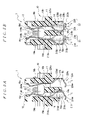
- Prior Art FIG. 8 is known to be an electrical connector of the type described above.
- Prior Art FIG. 8 is a cross-sectional view of a conventional electrical connector of the type described above.
- the electrical connector 101 shown in Prior Art FIG. 8 comprises an insulating housing 110 and a plurality of contacts 120 made of metal that are attached to the housing 110 .
- the housing 110 comprises a housing base part 111 that extends in the direction of length (direction perpendicular to the plane of the page in Prior Art FIG. 8 ) and a ridge part 112 that is provided in the central portion of the housing base part 111 in the direction of width (left-right direction in Prior Art FIG. 8 ) and that protrudes upward from the housing base part 111 and extends in the direction of length.
- each of the contacts 120 comprises a first plate part 121 and a second plate part 122 that are folded back at one end on the mating side, and is disposed in the housing 110 such that the first plate part 121 is on the outside, and the second plate part 122 is on the inside.
- the first plate part 121 of each contact 120 is provided with a fastening part 123 , a contact part 124 , and a connecting part 125 .
- the fastening part is press-fitted in the housing 110 .
- the contact part extends upward from the fastening part 123 and contacts a mating contact of a mating connector (not shown in the figure).
- the connecting part 125 extends downward from the fastening part 123 and is connected to a circuit board (not shown in the figure).
- the connecting part 125 comprises a first elastic part 125 a , a second elastic part 125 b , and an elastic contact part 125 c .
- the first elastic part 125 a extends in a straight line from the lower end of the fastening part 123 diagonally toward the outside at a small angle off vertical.
- the second elastic part 125 b extends in a straight line from the lower end of the first elastic part 125 a diagonally toward the outside at a large angle off vertical.
- the elastic contact part 125 c is provided at the tip end of the second elastic part 125 b and elastically contacts a conductive pad on the circuit board.
- the elastic contact parts 125 c of the contacts 120 in each row are arranged so as to form a straight line along the direction of length of the housing 110 (row direction of the contacts 120 ).
- the electrical connector 101 constructed in this manner is secured to the surface of the circuit board by mounting the housing 110 to the circuit board using fixing screws (not shown in the figure) or the like, and the elastic contact parts 125 c of the respective contacts 120 elastically contact the conductive pads on the circuit board. Furthermore, when the mating connector is caused to mate with the ridge part 112 of the electrical connector 101 while the electrical connector 101 is secured to the surface of the circuit board, the mating contacts make contact with the contact parts of the respective contacts 120 , so that the mating contacts and the conductive pads on the circuit board are electrically connected.
- the electrical connector shown in Prior Art FIG. 9 is known to be an electrical connector in which an elastic contact part that elastically contacts to a circuit board is provided, not on a contact, but on a shield (see JP03-012,383U).
- Prior Art FIG. 9 is a cross-sectional view of another conventional electrical connector.
- the electrical connector 201 shown in Prior Art FIG. 9 comprises an insulating housing 210 , a plurality of contacts 220 made of metal that are attached to the housing 210 , and a shield 230 made of metal that covers the housing 210 .
- the plurality of contacts 220 are arranged in two rows along the direction of length of the housing 210 (direction perpendicular to the plane of the page in Prior Art FIG. 9 ).
- Each of the contacts 220 comprises an elastic contact part 221 and a terminal part 222 .
- the elastic contact part 221 contacts a first circuit board 250 on the upper side.
- the terminal part contacts a mating contact 241 provided on a mating connector 240 on the lower side.
- the mating connector 240 is mounted on a second circuit board 260 .
- the metal shield 230 covers the housing 210 , and a first elastic contact part 231 and a second elastic contact part 232 that elastically contact conductive pads provided on the second circuit board 260 are provided at the lower ends of both sides of the housing 210 in the direction of width (both sides in the left-right direction in Prior Art FIG. 9 ).
- the first elastic contact part 231 is designed to extend in a straight line from the lower end of the shield 230 diagonally toward the outside and to elastically contact a conductive pad (not shown in the figure) formed on the second circuit board 260 .
- the second elastic contact part 232 is designed to be bent inward after extending outward from the lower end of the shield 230 and to elastically contact a conductive pad (not shown in the figure) formed on the second circuit board 260 with the tip end of this second elastic contact part 232 .
- the elastic contact parts 125 c tend not to contact the conductive pads.
- the elastic contact parts 125 c do not contact the conductive pads because of the dimensional tolerance of each contact 120 , errors in attachment to the housing 110 , the accumulation of the dimensional tolerances of the conductive pads in the direction of length of the housing 110 , or the like.
- the second elastic contact parts 232 extend outward from the lower end of the shield 230 , are then bent inward, and contact conductive pads formed on the second circuit board 260 with the tip ends thereof, therefore, this contributes to a reduction in the space required for forming the conductive pads in the direction of width of the electrical connector 201 .
- the first elastic contact parts 231 still extend in a straight line from the lower end of the shield 230 diagonally toward the outside, and elastically contact conductive pads formed on the second circuit board 260 , a large space is required for forming the conductive pads that contact the first elastic contact parts 231 in the direction of width of the housing 210 .
- the present invention in one embodiment among others, relates to a board mount-type connector having an insulative housing with a base and a row of contacts carried by the housing.
- Each contact has a centerpiece secured to the housing along a substantially vertically upright inner wall of the base, a mating interface connected to one end of the centerpiece so that the mating interface contacts a mating contact, and a board interface connected to the remaining end of the centerpiece so that the board interface connects to a circuit board.
- Each board interface has a bend that initially extends away from an extension line associated with a generally vertically upright portion of the respective centerpiece and that is bent back toward the extension line.
- a pad interface extends from the free end of the board interface toward the extension line and the contacts of the row are staggered along a length of the row.
- FIG. 1 is a front view of the board mount-type connector of the present invention
- FIG. 2 is a plan view of the board mount-type connector of FIG. 1 ;
- FIG. 3 is a bottom view of the board mount-type connector of FIG. 1 ;
- FIG. 4 is a left side view of the board mount-type connector of FIG. 1 ;
- FIG. 5A is a cross-sectional view along line 5 A- 5 A in FIG. 1 of the board mount-type connector of FIG. 1 ;
- FIG. 5B is a cross-sectional view along line 5 B- 5 B in FIG. 1 of the board mount-type connector of FIG. 1 ;
- FIG. 6 is a cross-sectional view in a state in which a board mount-type connector assembly is connected to a circuit board;
- FIG. 7 is a schematic plan view of conductive pads formed on the circuit board
- FIG. 8 is a sectional view of a conventional example of an electrical connector.
- FIG. 9 is a sectional view of another conventional example of an electrical connector.
- a board mount-type connector (hereafter simply referred to as “connector”) 1 shown in FIGS. 1 through 5 comprises an insulating housing 10 having first-row contacts 21 and second-row contacts 22 that are secured to the housing 10 in two rows.
- the housing 10 comprises a base 11 that extends in the direction of length (left-right direction in FIG. 1 ) and a mating wall 12 that extends along the direction of length of the base 11 and that protrudes upward (upward in FIG. 1 ) from the base 11 .
- the housing 10 is formed by molding an insulative resin.
- a mating recess 13 that extends along the direction of length of the mating wall 12 and that receives a mating part of a mating connector (not shown in the figures) is formed in the mating wall 12 of the housing 10 .
- FIGS. 1 the housing 10 comprises a base 11 that extends in the direction of length (left-right direction in FIG. 1 ) and a mating wall 12 that extends along the direction of length of the base 11 and that protrudes upward (upward in FIG. 1 ) from the base 11 .
- the housing 10 is formed by molding an insulative resin.
- a mating recess 13 that extends along the direction of length of the mating wall 12 and that
- a first contact recess 15 a is formed in the front side (left side in FIG. 5A ) of a partition wall 14 that extends in the direction of length
- a second contact recess 15 b is formed in the rear side of the partition wall 14 .
- the first contact recess 15 a and second contact recess 15 b both extend along the direction of length of the base 11 .
- a plurality of first-row contact securing holes 18 a that pass through toward the first contact recess 15 a and a plurality of second-row contact securing holes 18 b that pass through toward the second contact recess 15 b are formed in the bottom portion of the mating recess 13 .
- the first-row contact securing holes 18 a and second-row contact securing holes 18 b are respectively formed at a specified pitch along the direction of length of the base 11 .
- the first-row contact securing holes 18 a and second-row contact securing holes 18 b are formed in mutually facing positions in the direction of length of the base 11 .
- a plurality of first-row contact receiving grooves 19 a that respectively extend upward from the first-row contact securing holes 18 a are formed to the front side of the mating recess 13 .
- a plurality of second-row contact receiving grooves 19 b that respectively extend upward from the second-row contact securing holes 18 b are formed to the rear side of the mating recess 13 .
- first and second press-fitting posts 31 and 32 used with respect to a frame 40 are provided on both ends of the housing 10 in the direction of length.
- the first-row contacts 21 comprise first contacts 21 A and second contacts 21 B that are secured alternately at a specified pitch along the front side of the mating recess 13 .
- each of the first contacts 21 A comprises a first centerpiece 21 Aa, a first mating interface 21 Ab, and a first board interface 21 Ac.
- the first centerpiece 21 Aa is secured to an individual first-row contact securing hole 18 a .
- the first mating interface 21 Ab is provided on the upper side of the first centerpiece 21 Aa and contacts a mating contact (not shown in the figures).
- the first board interface 21 Ac is provided on the lower side of the first centerpiece 21 Aa and is to be connected to a circuit board PCB (see FIG. 6 ).
- Each first contact 21 A is formed by stamping and forming a conductive sheet metal having elasticity.
- the first mating interface 21 Ab extends upward from the upper end of the first centerpiece 21 Aa so as to protrude into the mating recess 13 , and the tip end of the first mating interface 21 Ab engages with a projection provided on the mating wall 12 of the housing 10 , so that a preload is applied.
- the first mating interface 21 Ab is located in a position corresponding to a first-row contact receiving groove 19 a , and can therefore be displaced inside the first-row contact receiving groove 19 a . Furthermore, as is shown in FIG.
- the first board interface 21 Ac comprises a first bend 21 Ad that is bent inward (forward) after extending outward (rearward) from the lower end of the first centerpiece 21 Aa, and a first pad interface 21 Ae that extends from the tip end of the first bend 21 Ad toward the extension line L of the first centerpiece 21 Aa.
- the extension line L of the first centerpiece 21 Aa extends substantially vertically down from the inner wall of base 11 against which inner wall the first centerpiece 21 Aa is generally at least partially abutted against.
- the first bend 21 Ad is formed with a thickness that is constant and smaller than the thickness of the first centerpiece 21 Aa.
- the first pad interface 21 Ae elastically contacts a conductive pad PA (see FIG. 7 ) formed on the circuit board PCB.
- the first pad interface 21 Ae extends toward the opposite side of the first bend 21 Ad (forward) beyond the extension line L of the first centerpiece 21 Aa. Furthermore, first bend grooves 16 a for allowing the first bent parts 21 Ad to be respectively positioned and displaced are formed in the front surface of the partition wall 14 of the housing 10 .
- each of the second contacts 21 B comprises a second centerpiece 21 Ba that is secured to an individual first-row contact securing hole 18 a , a second mating interface 21 Bb that is provided on the upper side of the second centerpiece 21 Ba and that contacts a mating contact (not shown in the figures), and a second board interface 21 Bc that is provided on the lower side of the second centerpiece 21 Ba and that is to be connected to the circuit board PCB.
- Each second contact 21 B is formed by stamping and forming a conductive sheet metal having elasticity.
- the second mating interface 21 Bb extends upward from the upper end of the second centerpiece 21 Ba so as to protrude into the mating recess 13 , and the tip end of the second mating interface 21 Bb engages with a projection provided on the mating wall 12 of the housing 10 , so that a preload is applied.
- the second mating interface 21 Bb is located in a position corresponding to a first-row contact receiving groove 19 a , and can therefore be displaced inside the first-row contact receiving groove 19 a . Furthermore, the position of the second mating interface 21 Bb that contacts a mating contact is shifted in the vertical direction from the position of the first mating interface 21 Ab that contacts a mating contact. In addition, as is shown in FIG.
- the second board interface 21 Bc comprises a second bend 21 Bd that is bent inward (rearward) after extending outward (forward) from the lower end of the second centerpiece 21 Ba, and an elastic second pad interface 21 Be that extends from the tip end of the second bend 21 Bd toward the extension line L of the second centerpiece 21 Ba.
- the extension line L of the second centerpiece 21 Ba extends substantially vertically down from the inner wall of base 11 against which inner wall the second centerpiece 21 Ba is generally at least partially abutted against.
- the second bend 21 Bd is formed with a thickness that is constant and smaller than the thickness of the second centerpiece 21 Ba.
- the second pad interface 21 Be elastically contacts a conductive pad PB formed on the circuit board PCB.
- the second pad interface 21 Be extends toward the opposite side of the second bend 21 Bd (rearward) beyond the extension line L of the second centerpiece 21 Ba. Furthermore, first cutouts 17 a for allowing the second bends 21 Bd to be respectively positioned and displaced are formed in the front wall of the first recessed part 15 a of the housing 10 .
- first bends 21 Ad of the first contacts 21 A respectively extend rearward from the lower ends of the first centerpieces 21 Aa, and are then bent forward
- second bends 21 Bd of the second contacts 21 B respectively extend forward from the lower ends of the second centerpieces 21 Ba, and are then bent rearward.
- the first and second bends 21 Ad and 21 Bd are arranged in a staggered fashion along the row direction of the first-row contacts 21 .
- first pad interfaces 21 Ae respectively extend toward the opposite side of the first bends 21 Ad (forward) beyond the extension line L of the first centerpieces 21 Aa, while the second pad interfaces 21 Be respectively extend toward the opposite side of the second bends 21 Bd (rearward) beyond the extension line L of the second centerpieces 21 Ba.
- first and second pad interfaces 21 Ae and 21 Be are arranged in a staggered fashion along the row direction of the first-row contacts 21 .
- first and second pad interfaces 21 Ae and 21 Be are arranged in a staggered fashion along the row direction of the first-row contacts 21 , it is not necessarily needed that the first pad interfaces 21 Ae respectively extend toward the opposite side of the first bends 21 Ad beyond the extension line L of the first centerpieces 21 Aa, nor that the second pad interfaces 21 Be respectively extend toward the opposite side of the second bends 21 Bd beyond the extension line L of the second centerpieces 21 Ba.
- the second-row contacts 22 have third contacts 22 A and fourth contacts 22 B that are secured alternately at a specified pitch along the rear wall of the mating recess 13 .
- the third contacts 22 A are disposed respectively facing the first contacts 21 A in the front-back direction of the connector 1 .
- each of the third contacts 22 A comprises a third centerpiece 22 Aa that is secured to an individual second-row contact securing hole 18 b , a third mating interface 22 Ab that is provided on the upper side of the third centerpiece 22 Aa and that contacts a mating contact (not shown in the figures), and a third board interface 22 Ac that is provided on the lower side of the third centerpiece 22 Aa and that is to be connected to the circuit board PCB.
- Each third contact 22 A is formed by stamping and forming a conductive sheet metal having elasticity.
- the third mating interface 22 Ab extends upward from the upper end of the third centerpiece 22 Aa so as to protrude into the mating recess 13 , and the tip end of the third mating interface 22 Ab engages with a projection provided on the mating wall 12 of the housing 10 , so that a preload is applied.
- the third mating interface 22 Ab is located in a position corresponding to a second-row contact receiving groove 19 b , and can therefore be displaced inside the second-row contact receiving groove 19 b . Furthermore, the position of the third mating interface 22 Ab that contacts a mating contact is shifted in the vertical direction from the position of the first mating interface 21 Ab that contacts a mating contact. Moreover, as is shown in FIG.
- the third board interface 22 Ac comprises a third bend 22 Ad that is bent inward (forward) after extending outward (rearward) from the lower end of the third centerpiece 22 Aa, and an third pad interface 22 Ae that extends from the tip end of the third bend 22 Ad toward the extension line L of the third centerpiece 22 Aa.
- the extension line L of the third centerpiece 22 Aa extends substantially vertically down from the inner wall of base 11 against which inner wall the first centerpiece 22 Aa is generally at least partially abutted against.
- the third bend 22 Ad is formed with a thickness that is constant and smaller than the thickness of the third centerpiece 22 Aa.
- the third pad interface 22 Ae elastically contacts a conductive pad PA formed on the circuit board PCB.
- the third pad interface 22 Ae extends toward the opposite side of the third bend 22 Ad (forward) beyond the extension line L of the third centerpiece 22 Aa. Furthermore, second cutouts 17 b for allowing the third bends 22 Ad to be respectively positioned and displaced are formed in the rear wall of the second recessed part 15 b of the housing 10 .
- each of the fourth contacts 22 B is disposed respectively facing the second contacts 21 B in the front-back direction of the connector 1 .
- each of the fourth contacts 22 B comprises a fourth centerpiece 22 Ba that is secured to an individual second-row contact securing hole 18 b , a fourth mating interface 22 Bb that is provided on the upper side of the fourth centerpiece 22 Ba and that contacts a mating contact (not shown in the figures), and a fourth board interface 22 Bc that is provided on the lower side of the fourth centerpiece 22 Ba and that is to be connected to the circuit board PCB.
- Each fourth contact 22 B is formed by stamping and forming a conductive sheet metal having elasticity.
- the fourth mating interface 22 Bb extends upward from the upper end of the fourth centerpiece 22 Ba so as to protrude into the mating recess 13 , and the tip end of the fourth mating interface 22 Bb engages with a projection provided on the mating wall 12 of the housing 10 , so that a preload is applied.
- the fourth mating interface 22 Bb is located in a position corresponding to a second-row contact receiving groove 19 b , and can therefore be displaced inside the second-row contact receiving groove 19 b . Furthermore, the position of the fourth mating interface 22 Bb that contacts a mating contact is shifted in the vertical direction from the position of the third mating interface 22 Ab of the third contact 22 A that contacts a mating contact. In addition, as is shown in FIG.
- the fourth board interface 22 Bc comprises a fourth bend 22 Bd that is bent inward (rearward) after extending outward (forward) from the lower end of the fourth centerpiece 22 Ba, and an elastic fourth pad interface 22 Be that extends from the tip end of the fourth bend 22 Bd toward the extension line L of the fourth centerpiece 22 Ba.
- the extension line L of the fourth centerpiece 22 Ba extends substantially vertically down from the inner wall of base 11 against which inner wall the first centerpiece 22 Ba is generally at least partially abutted against.
- the fourth bend 22 Bd is formed with a thickness that is constant and smaller than the thickness of the fourth centerpiece 22 Ba.
- the fourth pad interface 22 Be elastically contacts a conductive pad PB formed on the circuit board PCB.
- the fourth pad interface 22 Be extends toward the opposite side of the fourth bend 22 Bd (rearward) beyond the extension line L of the fourth centerpiece 22 Ba. Furthermore, second bend grooves 16 b for allowing the fourth bends 22 Bd to be respectively positioned and displaced are formed in the rear surface of the partition wall 14 of the housing 10 .
- the third bends 22 Ad of the third contacts 22 A respectively extend rearward from the lower ends of the third centerpieces 22 Aa, and are then bent forward
- the fourth bends 22 Bd of the fourth contacts 22 B respectively extend forward from the lower ends of the fourth centerpieces 22 Ba, and are then bent rearward.
- the third and fourth bends 22 Ad and 22 Bd are arranged in a staggered fashion along the row direction of the second-row contacts 22 .
- the third pad interfaces 22 Ae respectively extend toward the opposite side of the third bends 22 Ad (forward) beyond the extension line L of the third centerpieces 22 Aa, while the fourth pad interfaces 22 Be respectively extend toward the opposite side of the fourth bends 22 Bd (rearward) beyond the extension line L of the fourth centerpieces 22 Ba.
- the third and fourth pad interfaces 22 Ae and 22 Be are arranged in a staggered fashion along the row direction of the second-row contacts 22 .
- third and fourth pad interfaces 22 Ae and 22 Be are arranged in a staggered fashion along the row direction of the second-row contacts 22 , it is not necessarily needed that the third pad interfaces 22 Ae respectively extend toward the opposite side of the third bends 22 Ad beyond the extension line L of the third centerpieces 22 Aa, nor that the fourth pad interfaces 22 Be respectively extend toward the opposite side of the fourth bends 22 Bd beyond the extension line L of the fourth centerpieces 22 Ba.
- FIG. 7 is a schematic plan view of conductive pads formed on the circuit board.
- the conductive pads PA and PB formed on the circuit board PCB are formed in two rows corresponding to the first-row contacts 21 and second-row contacts 22 (only the conductive pads PA and PB in the first row are shown in FIG. 7 ). Furthermore, the conductive pads PA and PB in the first row are arranged in a staggered fashion at a pitch p along the row direction so as to be contacted by the first and second pad interfaces 21 Ae and 21 Be of the first-row contacts 21 , and the conductive pads PA and PB in the second row are also arranged in a staggered fashion at the pitch p along the row direction so as to be contacted by the third and fourth pad interfaces 22 Ae and 22 Be of the second-row contacts 22 .
- the first, second, third, and fourth pad interfaces 21 Ae, 21 Be, 22 Ae, and 22 Be which respectively extend toward the extension lines L of the first, second, third, and fourth centerpieces 21 Aa, 21 Ba, 22 Aa, and 22 Ba of the first-row contacts 21 and second-row contacts 22 from the tip ends of the first, second, third, and fourth bends 21 Ad, 21 Bd, 22 Ad, and 22 Bd that are bent inward after extending outward from the first, second, third, and fourth centerpieces 21 Aa, 21 Ba, 22 Aa, and 22 Ba contact the conductive pads PA and PB in the respective rows. Therefore, there is no increase in the space required for forming the conductive pads PA and PB on the circuit board PCB in the inward-outward direction (front-back direction) of the connector 1 .
- first, second, third, and fourth pad interfaces 21 Ae, 21 Be, 22 Ae, and 22 Be of the first-row contacts 21 and second-row contacts 22 are respectively arranged in a staggered fashion along the row direction of the contacts 21 and 22 , and the conductive pads PA and PB in each row are arranged in a staggered fashion along the row direction corresponding to these elastic contact parts.
- the respective conductive pads PA and PB correspond to the multi-position first, second, third, and fourth pad interfaces 21 Ae, 21 Be, 22 Ae, and 22 Be in a state in which the width of the respective conductive pads PA and PB contacted by the first, second, third, and fourth pad interfaces 21 Ae, 21 Be, 22 Ae, and 22 Be is large, there is no increase in the space required for forming the conductive pads PA and PB in the row direction of the first-row contacts 21 and second-row contacts 22 .
- the width of each of the conductive pads P must be reduced. If the width of each of the conductive pads P is reduced, when numerous connectors are simultaneously connected to a circuit board, in particular, there are cases in which the elastic contact parts do not contact the conductive pads P because of the dimensional tolerance of each contact, errors in attachment to the housing, the accumulation of the dimensional tolerances of the conductive pads P in the row direction of the conductive pads P, or the like.
- This problem can be avoided by respectively arranging the first, second, third, and fourth pad interfaces 21 Ae, 21 Be, 22 Ae, and 22 Be of the first-row contacts 21 and second-row contacts 22 in a staggered fashion along the row direction of the first-row contacts 21 and second-row contacts 22 , and arranging the conductive pads PA and PB in each row in a staggered fashion along the row direction corresponding to these elastic contact parts.
- connectors 1 are prepared in order to connect the numerous connectors 1 simultaneously to a circuit board PCB, and each connector 1 is accommodated and secured inside a connector accommodating hole 41 in the frame 40 as shown in FIG. 6 .
- the respective connectors 1 are secured inside the connector accommodating holes 41 in the frame 40 by press-fitting into the frame 40 the first and second press-fitting posts 31 and 32 provided on both ends of the housing 10 in the direction of length.
- a board mount-type connector assembly (connector assembly) 30 is completed.
- stoppers 43 are formed so as to protrude inward from each connector accommodating hole 41 in the frame 40 .
- the first, second, third, and fourth pad interfaces 21 Ae, 21 Be, 22 Ae, and 22 Be of the connectors 1 are respectively caused to elastically contact the conductive pads PA and PB formed on the circuit board PCB, and fixing screws 44 are passed through through-holes PCB 1 formed in the circuit board PCB, and are engaged with screw holes 42 in the frame 40 .
- the connection of the connectors 1 to the circuit board PCB is completed.
- the mating contacts make contact with the first and second mating interfaces 21 Ab and 21 Bb of the first-row contacts 21 and the third and fourth mating interfaces 22 Ab and 22 Bb of the second-row contacts 22 , so that the mating contacts and the conductive pads PA and PB on the circuit board PCB are electrically connected.
- the first, second, third, and fourth pad interfaces 21 Ae, 21 Be, 22 Ae, and 22 Be of the first-row contacts 21 and second-row contacts 22 respectively extend from the tip ends of the first, second, third, and fourth bends 21 Ad, 21 Bd, 22 Ad, and 22 Bd that are bent inward after extending outward from the first, second, third, and fourth centerpieces 21 Aa, 21 Ba, 22 Aa, and 22 Ba secured to the housing 10 . Therefore, the spring length is long, so that it is possible to obtain a sufficient amount of displacement when the first, second, third, and fourth bends 21 Ad, 21 Bd, 22 Ad, and 22 Bd are elastically deformed. This makes it possible to produce first-row contacts 21 and second-row contacts 22 that can withstand numerous repetitious connections to a circuit board PCB.
- first, second, third, and fourth pad interfaces 21 Ae, 21 Be, 22 Ae, and 22 Be respectively extend toward the opposite sides of the first, second, third, and fourth bends 21 Ad, 21 Bd, 22 Ad, and 22 Bd beyond the extension lines L of the first, second, third, and fourth centerpieces 21 Aa, 21 Ba, 22 Aa, and 22 Ba.
- first, second, third, and fourth pad interfaces 21 Ae, 21 Be, 22 Ae, and 22 Be elastically contact the conductive pads PA and PB on the circuit board PCB, it is possible to ensure wiping of the first, second, third, and fourth pad interfaces 21 Ae, 21 Be, 22 Ae, and 22 Be,—that is, in the case of the elastic contact parts Ae, for example, sliding to the leftward direction away from the extension line L.
- the thickness of the first, second, third, and fourth bends 21 Ad, 21 Bd, 22 Ad, and 22 Bd is made to be smaller than the thickness of the first, second, third, and fourth centerpieces 21 Aa, 21 Ba, 22 Aa, and 22 Ba
- the internal stress distribution of the first, second, third, and fourth bends 21 Ad, 21 Bd, 22 Ad, and 22 Bd can be controlled, making it possible to avoid the concentration of the stress in the first, second, third, and fourth centerpieces 21 Aa, 21 Ba, 22 Aa, and 22 Ba that serve as the fixed ends of the first, second, third, and fourth bends 21 Ad, 21 Bd, 22 Ad, and 22 Bd, compared to a case in which the thickness of the first, second, third, and fourth bends 21 Ad, 21 Bd, 22 Ad, and 22 Bd is set to be constant and the same as that of the first, second, third, and fourth centerpieces 21 Aa, 21 Ba, 22 Aa, and 22 Ba. Consequently, first-row contacts 21 and second-row
- contacts are provided in one or more rows; it is not necessarily needed to provide contacts in two rows.
- first, second, third, and fourth bends 21 Ad, 21 Bd, 22 Ad, and 22 Bd with a thickness that is smaller than the thickness of the first, second, third, and fourth centerpieces 21 Aa, 21 Ba, 22 Aa, and 22 Ba; the thickness of these elastic contact parts may also be the same as that of the first, second, third, and fourth centerpieces 21 Aa, 21 Ba, 22 Aa, and 22 Ba.
Abstract
Description
Claims (20)
Priority Applications (1)
| Application Number | Priority Date | Filing Date | Title |
|---|---|---|---|
| US12/039,796 US7544067B1 (en) | 2008-02-29 | 2008-02-29 | Board mount-type connector and board mount-type connector assembly |
Applications Claiming Priority (1)
| Application Number | Priority Date | Filing Date | Title |
|---|---|---|---|
| US12/039,796 US7544067B1 (en) | 2008-02-29 | 2008-02-29 | Board mount-type connector and board mount-type connector assembly |
Publications (1)
| Publication Number | Publication Date |
|---|---|
| US7544067B1 true US7544067B1 (en) | 2009-06-09 |
Family
ID=40688644
Family Applications (1)
| Application Number | Title | Priority Date | Filing Date |
|---|---|---|---|
| US12/039,796 Active US7544067B1 (en) | 2008-02-29 | 2008-02-29 | Board mount-type connector and board mount-type connector assembly |
Country Status (1)
| Country | Link |
|---|---|
| US (1) | US7544067B1 (en) |
Cited By (4)
| Publication number | Priority date | Publication date | Assignee | Title |
|---|---|---|---|---|
| US20100068942A1 (en) * | 2008-09-16 | 2010-03-18 | Japan Aviation Electronics Industry, Limited | Connector unit |
| WO2015183381A1 (en) * | 2014-05-27 | 2015-12-03 | Applied Materials, Inc. | Retention and insulation features for lamp |
| US20190006778A1 (en) * | 2017-06-28 | 2019-01-03 | Amphenol Commercial Products (ChengDu) Co.LTD | Miniaturized High-Speed Plug-In Card Type Connector |
| CN114503367A (en) * | 2019-10-18 | 2022-05-13 | 株式会社村田制作所 | Connector with a locking member |
Citations (12)
| Publication number | Priority date | Publication date | Assignee | Title |
|---|---|---|---|---|
| US4648668A (en) * | 1986-06-26 | 1987-03-10 | Amp Incorporated | Zero insertion force card edge connector |
| JPH0312383U (en) | 1989-06-21 | 1991-02-07 | ||
| US5595490A (en) * | 1995-01-13 | 1997-01-21 | Teradyne, Inc. | Printed circuit board connectors |
| JPH11126667A (en) | 1997-10-23 | 1999-05-11 | Amp Japan Ltd | Electric contact |
| US5921787A (en) * | 1996-07-17 | 1999-07-13 | Minnesota Mining And Manufacturing Company | Board-to-board interconnection |
| US6036504A (en) * | 1996-12-27 | 2000-03-14 | Hon Hai Precision Ind. Co., Ltd. | Board-to-board connector assembly |
| US6059580A (en) * | 1997-10-30 | 2000-05-09 | Mitsumi Electric Co., Ltd. | Socket connector with laterally inserted contacts |
| US6178629B1 (en) * | 1997-05-06 | 2001-01-30 | Gryphics, Inc. | Method of utilizing a replaceable chip module |
| US6276942B1 (en) * | 1999-10-21 | 2001-08-21 | Hon Hai Precision Ind. Co., Ltd. | Terminal for board to board connector |
| US7241147B2 (en) * | 2004-04-12 | 2007-07-10 | Intel Corporation | Making electrical connections between a circuit board and an integrated circuit |
| US7297003B2 (en) * | 2003-07-16 | 2007-11-20 | Gryphics, Inc. | Fine pitch electrical interconnect assembly |
| USD581876S1 (en) * | 2008-02-29 | 2008-12-02 | Tyco Electronics Amp K.K. | Electrical connector |
-
2008
- 2008-02-29 US US12/039,796 patent/US7544067B1/en active Active
Patent Citations (13)
| Publication number | Priority date | Publication date | Assignee | Title |
|---|---|---|---|---|
| US4648668A (en) * | 1986-06-26 | 1987-03-10 | Amp Incorporated | Zero insertion force card edge connector |
| JPH0312383U (en) | 1989-06-21 | 1991-02-07 | ||
| US5595490A (en) * | 1995-01-13 | 1997-01-21 | Teradyne, Inc. | Printed circuit board connectors |
| US5921787A (en) * | 1996-07-17 | 1999-07-13 | Minnesota Mining And Manufacturing Company | Board-to-board interconnection |
| US6036504A (en) * | 1996-12-27 | 2000-03-14 | Hon Hai Precision Ind. Co., Ltd. | Board-to-board connector assembly |
| US6178629B1 (en) * | 1997-05-06 | 2001-01-30 | Gryphics, Inc. | Method of utilizing a replaceable chip module |
| JPH11126667A (en) | 1997-10-23 | 1999-05-11 | Amp Japan Ltd | Electric contact |
| US6059580A (en) * | 1997-10-30 | 2000-05-09 | Mitsumi Electric Co., Ltd. | Socket connector with laterally inserted contacts |
| US6276942B1 (en) * | 1999-10-21 | 2001-08-21 | Hon Hai Precision Ind. Co., Ltd. | Terminal for board to board connector |
| US7297003B2 (en) * | 2003-07-16 | 2007-11-20 | Gryphics, Inc. | Fine pitch electrical interconnect assembly |
| US7422439B2 (en) * | 2003-07-16 | 2008-09-09 | Gryphics, Inc. | Fine pitch electrical interconnect assembly |
| US7241147B2 (en) * | 2004-04-12 | 2007-07-10 | Intel Corporation | Making electrical connections between a circuit board and an integrated circuit |
| USD581876S1 (en) * | 2008-02-29 | 2008-12-02 | Tyco Electronics Amp K.K. | Electrical connector |
Cited By (8)
| Publication number | Priority date | Publication date | Assignee | Title |
|---|---|---|---|---|
| US20100068942A1 (en) * | 2008-09-16 | 2010-03-18 | Japan Aviation Electronics Industry, Limited | Connector unit |
| US7892037B2 (en) * | 2008-09-16 | 2011-02-22 | Japan Aviation Electronics Industry, Limited | Connector unit provided with connector having first and second contacts of different lengths and with mating connector having first and second mating contacts of different lengths |
| WO2015183381A1 (en) * | 2014-05-27 | 2015-12-03 | Applied Materials, Inc. | Retention and insulation features for lamp |
| US10026630B2 (en) | 2014-05-27 | 2018-07-17 | Applied Materials, Inc. | Retention and insulation features for lamp |
| US20190006778A1 (en) * | 2017-06-28 | 2019-01-03 | Amphenol Commercial Products (ChengDu) Co.LTD | Miniaturized High-Speed Plug-In Card Type Connector |
| US10637169B2 (en) * | 2017-06-28 | 2020-04-28 | Amphenol Commercial Products (ChengDu) Co. LTD | Miniaturized high-speed plug-in card type connector |
| CN114503367A (en) * | 2019-10-18 | 2022-05-13 | 株式会社村田制作所 | Connector with a locking member |
| CN114503367B (en) * | 2019-10-18 | 2023-06-20 | 株式会社村田制作所 | Connector with a plurality of connectors |
Similar Documents
| Publication | Publication Date | Title |
|---|---|---|
| US8257095B2 (en) | Connector | |
| CN109565135B (en) | Connector with a locking member | |
| CN109565134B (en) | Connector with a locking member | |
| US7273381B2 (en) | Plug connector | |
| US7931477B2 (en) | Low profile board-to-board connector mating pair with solder barrier | |
| US7857665B2 (en) | Electrical connector with improved contact arrangement | |
| US7955130B2 (en) | Electrical connector with shielding plates without mounting tail and grounding member | |
| US8308513B2 (en) | Electrical connector | |
| US20080296133A1 (en) | Connector | |
| US20090280658A1 (en) | Connector | |
| US7967638B1 (en) | Mezzanine connector with contact wafers having opposite mounting tails | |
| US10193260B1 (en) | Multi-contact connector | |
| US10381776B2 (en) | Connector assembly with an improved latch member having a shorter length | |
| US20050042924A1 (en) | Electrical connector having shielding plates | |
| CN109496377B (en) | Contact terminal | |
| JP2014170726A (en) | Electric connector assembly and electric connector used for the same | |
| US20110086552A1 (en) | Card edge connector with improved cover | |
| US7972180B2 (en) | Electrical connector | |
| US7544067B1 (en) | Board mount-type connector and board mount-type connector assembly | |
| EP1217696A1 (en) | Electrical connector | |
| US7980882B2 (en) | Electrical plug receiving connector | |
| US7300290B2 (en) | Electrical connector | |
| US8668511B2 (en) | Hermaphroditic electrical connector | |
| US6234809B1 (en) | Card connector | |
| US8183155B1 (en) | Lower profile connector assembly |
Legal Events
| Date | Code | Title | Description |
|---|---|---|---|
| AS | Assignment |
Owner name: TYCO ELECTRONICS AMP K.K., JAPAN Free format text: ASSIGNMENT OF ASSIGNORS INTEREST;ASSIGNORS:HATANO, TAKAHIRO;KIMURA, MAKIYA;REEL/FRAME:020584/0210 Effective date: 20080213 Owner name: ADVANTEST CORPORATION, JAPAN Free format text: ASSIGNMENT OF ASSIGNORS INTEREST;ASSIGNORS:TAKAMOTO, TOMOYUKI;SAKIYAMA, SHIN;SEKIZUKA, TAKASHI;REEL/FRAME:020584/0343 Effective date: 20080213 |
|
| AS | Assignment |
Owner name: ADVANTEST CORPORATION, JAPAN Free format text: ASSIGNMENT OF ASSIGNORS INTEREST;ASSIGNORS:TAKAMOTO, TOMOYUKI;SAKIYAMA, SHIN;SEKIZUKA, TAKASHI;REEL/FRAME:021610/0800 Effective date: 20080213 Owner name: TYCO ELECTRONICS AMP K.K., JAPAN Free format text: ASSIGNMENT OF ASSIGNORS INTEREST;ASSIGNORS:HATANO, TAKAHIRO;KIMURA, MAKIYA;REEL/FRAME:021610/0400 Effective date: 20080616 |
|
| STCF | Information on status: patent grant |
Free format text: PATENTED CASE |
|
| AS | Assignment |
Owner name: TYCO ELECTRONICS JAPAN G.K., JAPAN Free format text: CHANGE OF NAME;ASSIGNOR:TYCO ELECTRONICS AMP K.K.;REEL/FRAME:025325/0675 Effective date: 20090927 |
|
| AS | Assignment |
Owner name: ADVANTEST CORPORATION, JAPAN Free format text: ASSIGNMENT OF ASSIGNORS INTEREST;ASSIGNOR:TYCO ELECTRONICS JAPAN, G.K.;REEL/FRAME:029181/0825 Effective date: 20121005 |
|
| FEPP | Fee payment procedure |
Free format text: PAYOR NUMBER ASSIGNED (ORIGINAL EVENT CODE: ASPN); ENTITY STATUS OF PATENT OWNER: LARGE ENTITY |
|
| FPAY | Fee payment |
Year of fee payment: 4 |
|
| FPAY | Fee payment |
Year of fee payment: 8 |
|
| AS | Assignment |
Owner name: ADVANTEST CORPORATION, JAPAN Free format text: CHANGE OF ADDRESS;ASSIGNOR:ADVANTEST CORPORATION;REEL/FRAME:047987/0626 Effective date: 20181112 |
|
| MAFP | Maintenance fee payment |
Free format text: PAYMENT OF MAINTENANCE FEE, 12TH YEAR, LARGE ENTITY (ORIGINAL EVENT CODE: M1553); ENTITY STATUS OF PATENT OWNER: LARGE ENTITY Year of fee payment: 12 |