EP0803062B1 - Process and device for determining the layer thickness, the conductivity and/or the layer contact quality of layers deposited on substrates - Google Patents
Process and device for determining the layer thickness, the conductivity and/or the layer contact quality of layers deposited on substrates Download PDFInfo
- Publication number
- EP0803062B1 EP0803062B1 EP96900528A EP96900528A EP0803062B1 EP 0803062 B1 EP0803062 B1 EP 0803062B1 EP 96900528 A EP96900528 A EP 96900528A EP 96900528 A EP96900528 A EP 96900528A EP 0803062 B1 EP0803062 B1 EP 0803062B1
- Authority
- EP
- European Patent Office
- Prior art keywords
- layer
- temperature
- measured
- light
- thermal
- Prior art date
- Legal status (The legal status is an assumption and is not a legal conclusion. Google has not performed a legal analysis and makes no representation as to the accuracy of the status listed.)
- Expired - Lifetime
Links
- 238000000034 method Methods 0.000 title claims description 27
- 239000000758 substrate Substances 0.000 title claims description 26
- 230000008569 process Effects 0.000 title description 3
- 239000010410 layer Substances 0.000 claims description 146
- 238000005259 measurement Methods 0.000 claims description 24
- 239000003990 capacitor Substances 0.000 claims description 23
- 238000011156 evaluation Methods 0.000 claims description 9
- 230000003287 optical effect Effects 0.000 claims description 8
- 239000000463 material Substances 0.000 claims description 7
- 230000035515 penetration Effects 0.000 claims description 7
- 239000008186 active pharmaceutical agent Substances 0.000 claims description 3
- 239000002356 single layer Substances 0.000 claims description 3
- 230000003595 spectral effect Effects 0.000 claims description 3
- 238000007599 discharging Methods 0.000 claims description 2
- 238000001514 detection method Methods 0.000 claims 1
- 238000001914 filtration Methods 0.000 claims 1
- 238000009792 diffusion process Methods 0.000 description 27
- 238000000576 coating method Methods 0.000 description 11
- 238000010586 diagram Methods 0.000 description 9
- 239000011248 coating agent Substances 0.000 description 7
- 238000005286 illumination Methods 0.000 description 5
- 230000008859 change Effects 0.000 description 4
- 238000001816 cooling Methods 0.000 description 4
- 238000009826 distribution Methods 0.000 description 4
- 238000010438 heat treatment Methods 0.000 description 4
- 230000031700 light absorption Effects 0.000 description 4
- 239000007787 solid Substances 0.000 description 4
- 230000002123 temporal effect Effects 0.000 description 4
- 238000012360 testing method Methods 0.000 description 4
- 230000036962 time dependent Effects 0.000 description 4
- 230000010363 phase shift Effects 0.000 description 3
- 230000005855 radiation Effects 0.000 description 3
- 238000012935 Averaging Methods 0.000 description 2
- 238000010521 absorption reaction Methods 0.000 description 2
- 238000013459 approach Methods 0.000 description 2
- 238000012937 correction Methods 0.000 description 2
- 239000007788 liquid Substances 0.000 description 2
- 238000012544 monitoring process Methods 0.000 description 2
- 230000008901 benefit Effects 0.000 description 1
- 230000005540 biological transmission Effects 0.000 description 1
- 230000000052 comparative effect Effects 0.000 description 1
- 230000001419 dependent effect Effects 0.000 description 1
- 230000001066 destructive effect Effects 0.000 description 1
- 238000006073 displacement reaction Methods 0.000 description 1
- 230000005284 excitation Effects 0.000 description 1
- 230000006870 function Effects 0.000 description 1
- 238000009413 insulation Methods 0.000 description 1
- 239000004922 lacquer Substances 0.000 description 1
- 238000004519 manufacturing process Methods 0.000 description 1
- 238000000691 measurement method Methods 0.000 description 1
- 230000005693 optoelectronics Effects 0.000 description 1
- 238000003908 quality control method Methods 0.000 description 1
- 238000011158 quantitative evaluation Methods 0.000 description 1
- 230000009467 reduction Effects 0.000 description 1
- 238000000926 separation method Methods 0.000 description 1
- 230000004936 stimulating effect Effects 0.000 description 1
- 239000000126 substance Substances 0.000 description 1
- 238000012549 training Methods 0.000 description 1
- 238000012546 transfer Methods 0.000 description 1
- 230000001052 transient effect Effects 0.000 description 1
Images


Classifications
-
- G—PHYSICS
- G01—MEASURING; TESTING
- G01B—MEASURING LENGTH, THICKNESS OR SIMILAR LINEAR DIMENSIONS; MEASURING ANGLES; MEASURING AREAS; MEASURING IRREGULARITIES OF SURFACES OR CONTOURS
- G01B11/00—Measuring arrangements characterised by the use of optical techniques
- G01B11/02—Measuring arrangements characterised by the use of optical techniques for measuring length, width or thickness
- G01B11/06—Measuring arrangements characterised by the use of optical techniques for measuring length, width or thickness for measuring thickness ; e.g. of sheet material
- G01B11/0616—Measuring arrangements characterised by the use of optical techniques for measuring length, width or thickness for measuring thickness ; e.g. of sheet material of coating
- G01B11/0658—Measuring arrangements characterised by the use of optical techniques for measuring length, width or thickness for measuring thickness ; e.g. of sheet material of coating with measurement of emissivity or reradiation
-
- G—PHYSICS
- G01—MEASURING; TESTING
- G01N—INVESTIGATING OR ANALYSING MATERIALS BY DETERMINING THEIR CHEMICAL OR PHYSICAL PROPERTIES
- G01N21/00—Investigating or analysing materials by the use of optical means, i.e. using sub-millimetre waves, infrared, visible or ultraviolet light
- G01N21/84—Systems specially adapted for particular applications
- G01N21/8422—Investigating thin films, e.g. matrix isolation method
Definitions
- the invention relates to a method according to the Preamble of claim 1 and a device for Execution of the procedure.
- the invention In addition to spot measurement, the solution is also for Checking the spatial homogeneity of applied Layers. So the parameters of Layers of solid, liquid or powdery Materials are determined. It is also possible perform measurements on moving objects, without having to track the measuring device is. The latter is particularly useful for the application directly in production.
- the known measuring methods the thermal waves use, have a relatively long measurement time, because the amplitude and phase of the steady state a thermal wave used as measurement signals become.
- the thickness of a spatial homogeneously applied layer can be determined in which a laser beam is directed onto a sample and there with a first area of the coating unknown thickness heated. Following that after a predetermined time the spatial temperature distribution over another area of the coating measured and the measured temperature distribution compared with reference temperature distributions, which is a certain comparative sample with a equivalent coating represent what on the layer thickness or the insulation properties of the Coating can be closed.
- a major advantage of the solution according to the invention consists in the fact that the measurement also on moving objects can be carried out without a parallel tracking movement of the measuring system required is. This leads to a significant simplification of the measurement setup.
- the measuring accuracy can be significantly increased if the distance between the object to be measured, the photothermal detector and the light source can be kept at a constant distance by regulation using a suitable device.
- the distance to the object to be measured is permanently determined and the distance signal is fed to a control unit which activates the displacement device accordingly.
- the evaluation of the temporal temperature behavior in the layer is associated with a substantial reduction in the required measuring time compared to the known solutions.
- the wavelength of the light to be directed onto the layer to be characterized or the layer system is chosen so that the optical penetration depth D E is small for as many layer materials as possible in comparison to the layer thickness D S to be measured.
- the ratio D S / D E should be ⁇ 10.
- Light in the wavelength range from ultraviolet or infrared can be used for a large number of colored layers, which are also transparent in the visible spectral range.
- a pulsed laser that emits light of the respective wavelength or a broadband light source that is suitably spectrally filtered can be used as the light source.
- the light pulse duration can be set and varied.
- the light absorption takes place in a region of the layer to be assessed which is close to the surface and a correspondingly suitable wavelength is used.
- thermal diffusion a certain proportion of the light energy absorbed by the layer from the region near the surface of the layer, which is determined by the optical penetration depth D E , continues into the layer. This process essentially determines the temperature behavior of the layer.
- the decisive factor is how much of the absorbed light energy by thermal diffusion propagates further into the layer from the near-surface absorption area within the duration of the light pulse.
- the layer thickness D S is small compared to the illumination spot diameter D L , a one-dimensional heat diffusion can be assumed for a theoretical description.
- the diffusion time t D is defined as the time at which the layer surface temperature has dropped to the value 1 / e of the maximum temperature value T max .
- the diffusion time t D can also be used to determine the layer characteristics.
- the Light pulse duration can be varied. So leads a short one Light pulse to a relatively steep temperature rise compared to the temperature drop on the surface, by thermal diffusion in the Layer is caused. Lying light pulse duration and thermal diffusion time in a comparable order of magnitude behave temperature rise and fall corresponding. With a relatively small thermal Diffusion time in relation to the light pulse duration is a small increase in surface temperature and the maximum temperature is reached at the time of the maximum of the light pulse. As a result, the surface temperature of the Layer by the light pulse with respect to it Duration determined.
- thermal thermal conductivity can relatively easily determine the layer thickness through the evaluation of the temperature profile (temperature rise and / or temperature drop) or even the maximum temperature respectively. But it is also possible to have conductivity and evaluate layer thickness if the temperature behavior during the heating and cooling phase can theoretically be described with a model. This is possible if the layer structure as so-called "thermal capacitor" considered becomes.
- the beam diameter (spot size) and detected area can Diffusion in the normal or lateral direction relative to the surface of the layer.
- the Description can be theoretical, one-dimensional with Using Fick's equations.
- the layer thickness can be determined with a single constant pulse duration.
- the pulse duration can be adapted to the desired measuring speed.
- the temperature behavior on the surface depends on what the thermal conductivity (thermal resistance) of the entire layer system is and what thermal conductivity the substrate (heat sink) has. Adjacent layers or the adjacent substrate influence each other with regard to the cooling behavior. If there is a layer with a high thermal conductivity on a substrate or is arranged next to another layer with a low thermal conductivity, the surface of the first layer under consideration cools more slowly than if the adjacent layer or the substrate also have a good thermal conductivity.
- the temperature profile of the surface temperature depends on the entire layer system and changes in monotony ( curvature dT ( t ) German ) of the temperature curve T (t) are due to the differences in relation to the thermal conductivity of the individual layers of the layer system.
- the thermal conductivity and the layer thickness of the individual layers can be determined by empirical comparison with model layer systems or also by comparison with the theoretical description in the model of the "thermal capacitor" from the temperature characteristics of the entire layer system.
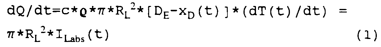
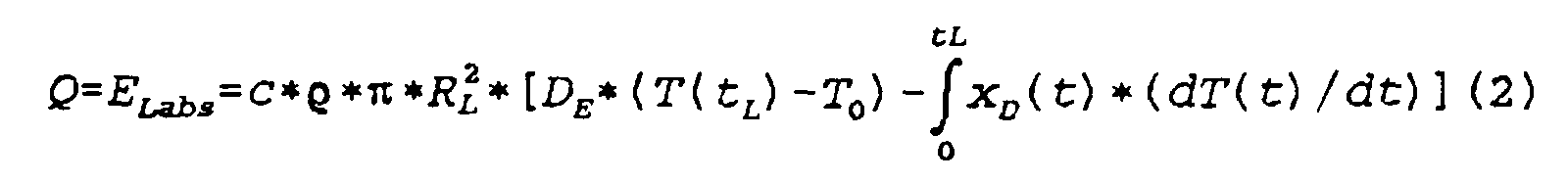
- Q is the thermal charge of the thermal capacitor after being charged by the light pulse.
- the charging can be described as follows: ⁇ 0 for t L ⁇ t D
- the absorbed light energy E Labs is absorbed in a certain volume, the volume being determined by the area of the illumination spot ( ⁇ * R L 2 ) and the optical penetration depth D E and the depth of the thermal diffusion x D (t L ) .
- variable determining the change in the temperature gradient is no longer the optical penetration depth D E ( ⁇ ) of the exciting light pulse, but the layer thickness D S.
- the thermal capacity corresponds to the electrical capacity C el .
- the temperature T (t) is equivalent to the electrical voltage U (t).
- a corresponding resistance R th and a capacitance C th can be assigned to each layer and the thermal capacitor model can be applied. It can be seen from equation (9) that the temperature drop occurs exponentially and that the exponent only contains the layer thickness D S as an unknown variable.
- the thermal capacitor is discharged via the thermal resistance of the substrate and the thermal resistance of the layer or, in the case of several layers, via the resistance of the entire layer system.
- the ratio of the thermal resistance of the substrate R A to the thermal resistance of the layer to be determined R S or the thermal resistance of the layer system determines the dynamics of the temperature characteristics when varying the layer thickness and conductivity single layer.
- the temperature drop is determined by the sheet resistance R S.
- a light pulse should be used whose pulse duration t L is small compared to the thermal diffusion time t D.
- the thermal resistance of the substrate R A is large compared to the resistance of the layer R s to be determined, the temperature drop on the surface of the measurement object (discharge of the thermal capacitor) is essentially determined by the thermal resistance of the substrate R A. In this case, therefore, the dynamics of the temperature drop of the surface of the measurement object are limited in relation to the detectable differences in layer thickness and conductivity of the layer. In such conditions, it is therefore preferable to use the heating of the surface of the test object, which is not influenced by the thermal resistance of the substrate R A.
- the ratio of the pulse duration of the light pulse t L with respect to the thermal diffusion time t D should therefore be optimized in order to achieve a maximum measuring speed and measuring dynamics. For this reason, the pulse duration must be set so that the difference between two temperature profiles, each with different layer thicknesses and conductivities, is maximized.
- the time Temperature characteristics such as the discharge time a capacitor, which can be calculated with a Network connected by different resistors is. For this, each shift becomes a very specific one Associated resistance.
- the time-dependent Discharge curve of the capacitor can be calculated, the is to be assigned to the respective layer, of which the thermal radiation with the photothermal detector is detected. Usually this will be the first Layer on the surface of the measurement object.
- Figure 1 shows schematically a known photothermal Measuring method in which modulated light blasted onto a layer applied to a substrate becomes.
- the absorption of the modulated light wave generates a thermal wave through the Layer propagates and at the layer / substrate interface is partially reflected.
- the reflected thermal wave produces a temporal modulation the layer surface temperature, which is a phase shift to the modulated light wave.
- in the steady state provides the phase shift between light wave and reflected thermal Wave, the desired layer thickness.
- the amplitude the reflected thermal wave is all the more greater the lower the contact quality between layers and is substrate. To determine these parameters is however, it requires a steady state is achieved. With layer thicknesses in the micrometer range is a measurement time of a few seconds what is required for many uses is slow.
- Figure 2 is an equivalent circuit diagram in which a single-layer structure on a substrate, such as a electrical capacitor is considered that over a resistor is discharged.
- Figure 3 represents the time-dependent discharge characteristic of the electrical Capacitor represents the time decay of the Surface temperature of the layer corresponds to that with was irradiated with a pulse of light.
- FIG. 4 shows a measurement setup according to the invention, in which a light pulse is emitted from a light source onto the layer 3 applied to a substrate 2 and the temperature influence thus caused is detected with the aid of a thermo-optical detector 4.
- the heated area 5 of the layer is shown in dashed lines. In the case shown, the pulse duration is much smaller than the diffusion time.
- the diameter of the laser excitation (illumination spot diameter) is adapted for a one-dimensional diffusion model.
- FIG. 5 schematically shows a two-layer system in which two layers 3 and 6 are applied to a substrate 2.
- the corresponding equivalent circuit diagram can be seen in FIG. 6.
- C 1 and R 1 are the thermal capacitor and resistance of layer 3 and R 2 are thermal resistance of layer 6.
- the "thermal capacitor” C 1 is discharged via the thermal resistances of layer 3 (resistor R 1 ), layer 6 ( Resistor R 2 ) and the thermal resistance of the substrate (resistance R a ).
- the diagram shown in FIG. 7 shows the temperature profile over time in the event that a very small light pulse duration t L compared to the characteristic diffusion time t D is set by briefly switching the light source on and off or with the aid of an optoelectronic or electromechanical shutter.
- the maximum temperature Tmax is reached after a short time.
- FIG. 8 shows a diagram of the temperature profile in the event that the light pulse duration approximately corresponds to the diffusion time t D.
- the light pulse duration is considerably longer than the diffusion time t D.
- the diagram shown in FIG. 10 is the temperature curve in a two-layer system, with a layer with good thermal conductivity and one Layer with poor thermal conductivity with a short one Light pulse duration, shown.
- During the temperature drop phase is clearly the change in the curvature reproduced in the temperature drop.
- a logarithmic evaluation increases the distinctness of the individual components of the layer system (Curve fitting with 2 exponents for the two layers and a third exponent for that Substrate). In the same way, polynomial matching be performed.
- FIG. 11 shows the temperature profile for a Two-layer system that consists of two layers with good Thermal conductivity, with the same thickness as in Figure 10 is formed again.
- the change in curvature is significantly less than in the case of the curve shown in FIG. 10 and the temperature drops much faster.
- FIG 12 is a schematic measurement setup of a Device shown according to the invention on which Measurement object 7 translationally along the dashed line drawn line is movable.
- the photothermal Measuring device 4 is translationally equivalent the direction shown with the double arrow (vertical movable to the direction of movement of the measurement object 7)
- Device 8 added and can with their help moved towards or away from the measurement object 7 be a constant measuring distance between photothermal Adhere to measuring device 4 and test object 7 can.
- the control is carried out with a distance measuring device 9, which optically prefers the distance detected.
- the measuring beams from optical distance measuring device and photothermal measuring device with stimulating Light pulse and registration photothermal detector are marked with a dot-dash line.
- the measuring signals (dotted lines) of the distance measuring device 9 are controlled by a controller 10 be given the drive 8 of the device.
- the dotted line from the photothermal measuring device 4 to the controller 10 shows that the Current position deviating from the ideal state of the photothermal measuring device 4 from the controller 10 recorded and for a numerical correction of the photothermal Measured values can be used.
- the direction the data transmission is shown in dotted lines Connections marked with arrows.
- the Data that can be output by controller 10 can be used for a Evaluation, for example in statistical form and / or directly for actively influencing the coating process used to on the Coating failure to respond and the coating to optimally adhere to the target values.
Landscapes
- Physics & Mathematics (AREA)
- General Physics & Mathematics (AREA)
- Biochemistry (AREA)
- Life Sciences & Earth Sciences (AREA)
- Chemical & Material Sciences (AREA)
- Analytical Chemistry (AREA)
- Health & Medical Sciences (AREA)
- General Health & Medical Sciences (AREA)
- Mathematical Physics (AREA)
- Immunology (AREA)
- Pathology (AREA)
- Investigating Or Analyzing Materials Using Thermal Means (AREA)
- Length Measuring Devices By Optical Means (AREA)
Description
Die Erfindung betrifft ein Verfahren nach dem
Oberbegriff des Anspruchs 1 und eine Vorrichtung zur
Durchführung des Verfahrens. Die erfindungsgemäße
Lösung ist neben der punktuellen Messung auch für die
Überprüfung der räumlichen Homogenität von aufgetragenen
Schichten geeignet. So können die Parameter von
Schichten aus festem, flüssigen oder pulverförmigen
Materialien bestimmt werden. Außerdem ist es möglich,
die Messung an bewegten Meßobjekten durchzuführen,
ohne daß eine Nachführung der Meßvorrichtung erforderlich
ist. Letzteres bietet sich insbesondere bei
der Anwendung direkt in der Produktion an.The invention relates to a method according to the
Preamble of
Es ist bekannt, photothermische Meßverfahren zur Beurteilung von Schichten, insbesondere der Schichtdikken zu verwenden. Hierbei werden modulierte, kontinuierlich emittierende Lichtquellen verwendet, die eine thermische Welle im Meßobjekt erzeugen. Die thermische Welle wird an der Schichtgrenze zumindest teilweise reflektiert, dabei kann die Schichtdicke mittels der Phasenverschiebung zwischen der von der modulierten Lichtquelle ausgehenden Welle und der reflektierten thermischen Welle ermittelt werden. Die Amplitude der reflektierten thermischen Welle ist ein Maß für die erreichte Schichtkontaktgüte. Außerdem ist es bekannt, gepulste Lichtquellen, deren Impulsdauer und spektrale Lichtverteilung nicht auf die Schichtart und Schichtdicke der Probe optimiert sind, zu verwenden, um Schichten und oberflächennahe Bereiche von Festkörpern zu untersuchen. Diese Verfahren sind nicht für eine genaue quantitative Auswertung zur Bestimmung von Schichtparametern geeignet.It is known to use photothermal measurement methods for assessment of layers, especially layer thicknesses to use. This modulates, continuously emitting light sources used one Generate thermal wave in the test object. The thermal Wave becomes at least partially at the layer boundary reflected, the layer thickness can be determined using the phase shift between that of the modulated Light source outgoing wave and the reflected thermal wave can be determined. The The amplitude of the reflected thermal wave is a Measure of the layer contact quality achieved. Moreover it is known pulsed light sources, their pulse duration and spectral light distribution does not affect that Layer type and layer thickness of the sample are optimized, to use layers and near-surface areas of solids. This procedure are not for accurate quantitative evaluation suitable for determining layer parameters.
Die bekannten Meßverfahren, die thermische Wellen verwenden, weisen eine relativ lange Meßzeit auf, da die Amplitude und Phase des eingeschwungenen Zustandes einer thermischen Welle als Meßsignale verwendet werden.The known measuring methods, the thermal waves use, have a relatively long measurement time, because the amplitude and phase of the steady state a thermal wave used as measurement signals become.
So haben S.K. Lau, D.B. Almond und P.M. Patel in "Transient thermal wave techniques for the evaluation of surface coatings", 1261 Journal of Physics D: Applied Physics, 24 (1991) 14 March, No. 3, Bristol, GB, Seiten 428 bis 436 ein Verfahren zur Bestimmung von Schichtdicken beschrieben, das auf der Interferenz von thermischen Wellen basiert. Dabei müssen die mittels bevorzugt einer Laserlichtquelle auf die oberflächen gerichteten Lichtstrahlen durch Wärmeleitung in der Schicht und Reflexion an den Schichtgrenzen mehrfach durch die Schicht laufen, um an der Oberfläche zu interferieren.So S.K. Lau, D.B. Almond and P.M. Patel in "Transient thermal wave techniques for the evaluation of surface coatings ", 1261 Journal of Physics D: Applied Physics, 24 (1991) March 14, No. 3, Bristol, GB, pages 428 to 436 a method for determination described by layer thicknesses based on the interference based on thermal waves. The preferably by means of a laser light source on the surface-directed light rays through heat conduction in the layer and reflection at the layer boundaries run through the shift several times to get to the Surface to interfere.
Ein weiteres Verfahren zur Bestimmung der Dicke von aufgetragenen Schichten ist in US 4,818,118 beschrieben. Bei diesem Verfahren soll die Dicke einer räumlich homogen aufgetragenen Schicht bestimmt werden, in dem ein Laserstrahl auf eine Probe gerichtet wird und dort einen ersten Bereich der Beschichtung mit unbekannter Dicke erwärmt. Im Anschluß daran wird nach einer vorgegebenen Zeit die räumliche Temperaturverteilung über einen anderen Bereich der Beschichtung gemessen und die gemessene Temperaturverteilung mit Referenztemperaturverteilungen verglichen, die eine bestimmte Vergleichsprobe mit einer äquivalenten Beschichtung repräsentieren, woraus auf die Schichtdicke oder die Isolationseigenschaften der Beschichtung geschlossen werden kann.Another method for determining the thickness of applied layers is described in US 4,818,118. In this method, the thickness of a spatial homogeneously applied layer can be determined in which a laser beam is directed onto a sample and there with a first area of the coating unknown thickness heated. Following that after a predetermined time the spatial temperature distribution over another area of the coating measured and the measured temperature distribution compared with reference temperature distributions, which is a certain comparative sample with a equivalent coating represent what on the layer thickness or the insulation properties of the Coating can be closed.
Es ist daher Aufgabe der Erfindung, ein Verfahren und eine Vorrichtung zu schaffen, mit der Parameter von auf Substraten aufgetragenen Schichten in kurzer Zeit mit ausreichender Genauigkeit bestimmt werden können.It is therefore an object of the invention, a method and to create a device with the parameters of layers applied to substrates in a short time can be determined with sufficient accuracy.
Erfindungsgemäß wird diese Aufgabe, durch die im Anspruch
1 für das Verfahren und die im kennzeichnenden
Teil des Anspruchs 11 für die Vorrichtung genannten
Merkmale, gelöst. Vorteilhafte Ausgestaltungen und
Weiterbildungen ergeben sich bei Verwendung der in
den untergeordneten Ansprüchen enthaltenen Merkmale.According to the invention, this object is achieved by the
Mit der erfindungsgemäßen Lösung können einzelne Schichten und Systeme solcher Schichten auf Festkörpersubstraten berührungslos und zerstörungsfrei charakterisiert werden. Dabei kann auf einfache Weise die Schichtdicke, die thermische Leitfähigkeit der Schicht oder die Schichtkontaktgüte an Grenzflächen benachbarter Schichten oder zum Substrat hin gemessen und bewertet werden. Das Verfahren und die erfindungsgemäße Vorrichtung können dabei direkt während des Beschichtungsprozesses von Substraten eingesetzt und die Meßergebnisse zur Steuerung des Beschichtungsprozesses herangezogen werden. Es kann aber auch im nachhinein in Form einer Qualitätskontrolle Verwendung finden.With the solution according to the invention, individual Layers and systems of such layers on solid substrates characterized non-contact and non-destructive become. It can be done in a simple way the layer thickness, the thermal conductivity of the Layer or the layer contact quality at interfaces neighboring layers or measured towards the substrate and be evaluated. The method and the invention Device can be used directly during the coating process of substrates and the measurement results to control the coating process be used. It can but also afterwards in the form of a quality control Find use.
Weiter sind neben punktuellen Messungen auch die Überwachung der räumlichen Homogenität durch linien- oder rasterartige, flächige Vermessung der Beschichtung möglich. Dabei spielt es keine Rolle, ob die Schichten aus festen, flüssigen oder pulverförmigen Stoffen gebildet sind.In addition to spot measurements, there are also Monitoring of spatial homogeneity using linear or grid-like, flat measurement of the coating possible. It does not matter whether the Layers of solid, liquid or powdery Substances are formed.
Ein wesentlicher Vorteil der erfindungsgemäßen Lösung besteht darin, daß die Messung auch an bewegten Meßobjekten durchgeführt werden kann, ohne daß eine parallele nachführende Bewegung des Meßsystems erforderlich ist. Dies führt zu einer wesentlichen Vereinfachung des Meßaufbaus.A major advantage of the solution according to the invention consists in the fact that the measurement also on moving objects can be carried out without a parallel tracking movement of the measuring system required is. This leads to a significant simplification of the measurement setup.
Wird die Meßkonfiguration mit einem Abstandsmeßgerät komplettiert, kann die Meßgenauigkeit wesentlich erhöht werden, wenn der Abstand zwischen Meßobjekt, photothermischen Detektor und Lichtquelle mit einer geeigneten Vorrichtung in einem konstanten Abstand durch Regelung gehalten werden kann. Dabei wird der Abstand zum Meßobjekt permanent ermittelt und das Abstandssignal einer Regeleinheit zugeführt, die die Verschiebevorrichtung entsprechend aktiviert. Mit der Auswertung des zeitlichen Temperaturverhaltens in der Schicht ist eine wesentliche Verkürzung der erforderlichen Meßzeit, gegenüber den bekannten Lösungen verbunden. Dabei wird die Wellenlänge, des auf die zu charakterisierende Schicht oder das Schichtsystem zu richtenden Lichtes so gewählt, daß die optische Eindringtiefe DE für möglichst viele Schichtmaterialien klein im Vergleich zur zu messenden Schichtdicke DS ist. Dabei sollte das Verhältnis DS/DE ≥ 10 sein. Licht im Wellenlängenbereich von Ultraviolett oder Infrarot kann für sehr viele farbige und auch im sichtbaren Spektralbereich transparente Schichten eingesetzt werden. Als Lichtquelle kommt ein gepulst arbeitender Laser, der Licht der jeweiligen Wellenlänge abstrahlt oder auch eine breitbandige Lichtquelle, die geeignet spektral gefiltert wird, in Frage. Mit einem elektrooptischen oder elektromechanischen Verschluß kann die Lichtimpulsdauer eingestellt und variiert werden. Bei der erfingsgemäßen Lösung ist es günstig, wenn die Lichtabsorption in einem oberflächennahen Bereich der zu bewertenden Schicht erfolgt und eine entsprechend geeignete Wellenlänge verwendet wird. Durch thermische Diffusion gelangt ein gewisser Anteil der von der Schicht absorbierten Lichtenergie aus dem oberflächennahen Bereich der Schicht, der durch die optische Eindringtiefe DE bestimmt ist, weiter in die Schicht hinein. Dieser Vorgang bestimmt im wesentlichen das Temperaturverhalten der Schicht. Für die Aufheizung der Schichtoberfläche ist entscheidend, wieviel von der absorbierten Lichtenergie durch thermische Diffusion innerhalb der Dauer des Lichtimpulses aus dem oberflächennahen Absorptionsbereich weiter in die Schicht propagiert.If the measuring configuration is completed with a distance measuring device, the measuring accuracy can be significantly increased if the distance between the object to be measured, the photothermal detector and the light source can be kept at a constant distance by regulation using a suitable device. The distance to the object to be measured is permanently determined and the distance signal is fed to a control unit which activates the displacement device accordingly. The evaluation of the temporal temperature behavior in the layer is associated with a substantial reduction in the required measuring time compared to the known solutions. The wavelength of the light to be directed onto the layer to be characterized or the layer system is chosen so that the optical penetration depth D E is small for as many layer materials as possible in comparison to the layer thickness D S to be measured. The ratio D S / D E should be ≥ 10. Light in the wavelength range from ultraviolet or infrared can be used for a large number of colored layers, which are also transparent in the visible spectral range. A pulsed laser that emits light of the respective wavelength or a broadband light source that is suitably spectrally filtered can be used as the light source. With an electro-optical or electromechanical shutter, the light pulse duration can be set and varied. In the solution according to the invention, it is advantageous if the light absorption takes place in a region of the layer to be assessed which is close to the surface and a correspondingly suitable wavelength is used. Through thermal diffusion, a certain proportion of the light energy absorbed by the layer from the region near the surface of the layer, which is determined by the optical penetration depth D E , continues into the layer. This process essentially determines the temperature behavior of the layer. For the heating of the layer surface, the decisive factor is how much of the absorbed light energy by thermal diffusion propagates further into the layer from the near-surface absorption area within the duration of the light pulse.
Ist die Schichtdicke DS klein im Vergleich zum Beleuchtungsfleckdurchmesser
DL kann für eine theoretische
Beschreibung, eine eindimensionale Wärmediffusion
angenommen werden. Bei im Verhältnis kleiner
Lichtimpulsdauer tL gegenüber der thermischen Diffusonszeit
tD, kann die thermische Diffusion während
der Lichtimpulsdauer, die zur Abkühlung an der Oberfläche
führt, gegenüber der Aufheizung der Oberfläche
durch Lichtabsorption vernachlässigt werden. Dabei
wird die Diffusionszeit tD als Zeit definiert, bei
der die Schichtoberflächentemperatur auf den Wert 1/e
des maximalen Temperaturwertes Tmax abgefallen ist.Die
Diffusionszeit tD kann ebenfalls zur Bestimmung der
Schichtcharakteristika herangezogen werden.If the layer thickness D S is small compared to the illumination spot diameter D L , a one-dimensional heat diffusion can be assumed for a theoretical description. With a relatively small light pulse duration t L compared to the thermal diffusion time t D , the thermal diffusion during the light pulse duration, which leads to cooling on the surface, can be neglected compared to the heating of the surface by light absorption. The diffusion time t D is defined as the time at which the layer surface temperature has dropped to the
Mit dem erfindungsgemäßen Verfahren kann die Lichtimpulsdauer variiert werden. So führt ein kurzer Lichtimpuls zu einem relativ steilen Temperaturanstieg im Vergleich zum Temperaturabfall an der Oberfläche, der durch die thermische Diffusion in der Schicht hervorgerufen wird. Liegen Lichtimpulsdauer und thermische Diffusionszeit in vergleichbarer Größenordnung verhalten sich Temperaturanstieg und Temperaturabfall entsprechend. Bei relativ kleiner thermischer Diffusionszeit im Verhältnis zur Lichtimpulsdauer ist ein geringer Anstieg der Oberflächentemperatur zu verzeichnen, und das Maximum der Temperatur wird zum Zeitpunkt des Maximum des Lichtimpulses erreicht. Demzufolge wird die Oberflächentemperatur der Schicht durch den Lichtimpuls in bezug auf dessen Zeitdauer bestimmt.With the method according to the invention, the Light pulse duration can be varied. So leads a short one Light pulse to a relatively steep temperature rise compared to the temperature drop on the surface, by thermal diffusion in the Layer is caused. Lying light pulse duration and thermal diffusion time in a comparable order of magnitude behave temperature rise and fall corresponding. With a relatively small thermal Diffusion time in relation to the light pulse duration is a small increase in surface temperature and the maximum temperature is reached at the time of the maximum of the light pulse. As a result, the surface temperature of the Layer by the light pulse with respect to it Duration determined.
Bei Variation der Lichtimpulsdauer werden zeitliche Charakteristiken des Oberflächentemperaturverlaufes T(t) erreicht, die proportional zur thermischen Leitfähigkeit und zur Schichtdicke der jeweiligen Schicht sind. Bei bekannter thermischer Wärmeleitfähigkeit kann relativ einfach die Schichtdicke durch die Auswertung des Temperaturverlaufes (Temperaturanstieg und/oder Temperaturabfall) oder gar der Maximaltemperatur erfolgen. Es ist aber auch möglich, Leitfähigkeit und Schichtdicke zu bewerten, wenn das Temperaturverhalten während der Aufheiz- und Abkühlphase theoretisch mit einem Modell beschrieben werden können. Möglich ist dies, wenn der Schichtaufbau als sogenannter "thermischer Kondensator" betrachtet wird.When the duration of the light pulse varies, temporal Characteristics of the surface temperature curve T (t) reached which is proportional to the thermal conductivity and the layer thickness of the respective layer are. With known thermal thermal conductivity can relatively easily determine the layer thickness through the evaluation of the temperature profile (temperature rise and / or temperature drop) or even the maximum temperature respectively. But it is also possible to have conductivity and evaluate layer thickness if the temperature behavior during the heating and cooling phase can theoretically be described with a model. This is possible if the layer structure as so-called "thermal capacitor" considered becomes.
Bei einem kurzen Lichtimpuls im Vergleich zur Diffusionszeit, ist der durch Strahlendurchmesser und optischer Eindringtiefe bestimmte Wärmestrom innerhalb der Lichtimpulsdauer klein. Für eine solche Konstellation wird das Abkühlverhalten ausgewertet. Liegen Lichtimpulsdauer und thermische Diffusionszeit in der gleichen Größenordnung, kann der gesamte Temperaturverlauf benutzt werden. Mit Variation der Lichtimpulsdauer kann das Temperaturverhalten zur Ermittlung der Schichtparameter ebenfalls ausgewertet werden.With a short light pulse compared to the diffusion time, is that by beam diameter and more optical Penetration depth determined heat flow within the light pulse duration is small. For such a constellation the cooling behavior is evaluated. Lie Light pulse duration and thermal diffusion time in the same order of magnitude, the entire temperature history to be used. With variation of the light pulse duration can determine the temperature behavior the shift parameters can also be evaluated.
Mittels Abstimmung von Strahldurchmesser (Beleuchtungsfleckgröße) und detektierten Bereich kann die Diffusion in normaler oder lateraler Richtung relativ zur Oberfläche der Schicht betrachtet werden. Die Beschreibung kann theoretisch, eindimensional mit Hilfe der Fick'schen Gleichungen erfolgen.By adjusting the beam diameter (spot size) and detected area can Diffusion in the normal or lateral direction relative to the surface of the layer. The Description can be theoretical, one-dimensional with Using Fick's equations.
Neben dieser Möglichkeit kann jedoch auch eine rein empirische Auswertung erfolgen, wobei charakteristische Temperaturverläufe, bei Variation von Impulsdauer oder Wellenlänge für definierte, bekannte Schichtdicken gemessen worden sind und diese Meßwerte mit in nachfolgenden Messungen ermittelten, in einem Speicher für einen Vergleich abgelegten Meßwerten (z.B. in Form von Temperaturverläufen) von unbekannten Schichten eines gleichartigen Schichtsystems verglichen werden. Die empirische Auswertung ist für eine direkte Prozeßüberwachung im industriellen Einsatz geeignet.In addition to this possibility, one can also be purely empirical evaluation take place, whereby characteristic Temperature curves, with variation of pulse duration or wavelength for defined, known layer thicknesses have been measured and these measured values with in subsequent measurements determined in a memory for a comparison of stored measured values (e.g. in the form of temperature profiles) from unknown Layers of a similar layer system compared become. The empirical evaluation is for one direct process monitoring in industrial use suitable.
Ist die thermische Leitfähigkeit des Materials der
Schicht bekannt, kann die Schichtdicke allein mit
einer einzigen konstanten Impulsdauer bestimmt werden.
Dabei kann die Impulsdauer an die gewünschte
Meßgeschwindigkeit angepaßt sein. Bei Schichtsystemen
hängt das Temperaturverhalten an der Oberfläche davon
ab, wie die thermische Leitfähigkeit (thermischer
Widerstand) des gesamten Schichtsystems ist und welche
Wärmeleitfähigkeit das Substrat (Wärmesenke) hat.
Benachbarte Schichten bzw. das benachbart angeordnete
Substrat beeinflussen sich, in bezug auf das Abkühlverhalten.
Befindet sich eine Schicht mit hoher thermischer
Leitfähigkeit auf einem Substrat oder ist
neben einer weiteren Schicht mit einer niedrigen Wärmeleitfähigkeit
angeordnet, kühlt sich die Oberfläche
der ersten betrachteten Schicht langsamer ab, als
wenn die benachbarte Schicht oder das Substrat
gleichfalls eine gute thermische Leitfähigkeit haben.
Daher ist der Temperaturverlauf der Oberflächentemperatur
vom gesamten Schichtsystem abhängig und Änderungen
der Monotonie
Nachfolgend soll das theoretische Modell des "thermischen Kondensators" weiter beschrieben werden:The theoretical model of the "thermal Capacitor "are further described:
Dabei ist Q die thermische Ladung des thermischen
Kondensators nach der Aufladung durch den Lichtimpuls.
Die Aufladung kann folgendermaßen beschrieben
werden:
Dabei sind :
- c
- spezifische Wärme des Schichtmaterials;
-

- Dichte des Schichtmaterials;
- π*RL 2
- Fläche des Beleuchtungsfleckes auf der Schicht;
- ILabs
- absorbierte Lichtintensität;
- ELabs
- absorbierte Lichtenergie;
- xD(t)
- Wärmediffusionsstrecke zur Zeit t
- tD=DS*DE*
- charakteristische Diffusionszeit;
- DS
- Schichtdicke;
- χ
- Wärmeleitfähigkeit der Schicht.
- T0
- Umgebungstemperatur
- c
- specific heat of the layer material;
-
- Density of the layer material;
- π * R L 2
- Area of the illumination spot on the layer;
- I labs
- absorbed light intensity;
- E Labs
- absorbed light energy;
- x D (t)
- Thermal diffusion path at time t
- t D = D S * D E *
- characteristic diffusion time;
- D S
- Layer thickness;
- χ
- Thermal conductivity of the layer.
- T 0
- Ambient temperature
Während der Impulsdauer wird die absorbierte Lichtenergie ELabs in einem bestimmten Volumen aufgenommen, wobei das Volumen durch die Fläche des Beleuchtungsfleckes (π*RL 2) und die optische Eindringtiefe DE und die Tiefe der thermischen Diffusion xD(tL) bestimmt wird. Mit der Annahme, daß tL sehr viel kleiner als die charakteristische Diffusionszeit tD ist, kann mit Gleichung (2) die maximale Temperatur Tmax = T(tL) aus der thermischen Ladung Q bestimmt werden. Dies ist möglich, da die anderen Parameter bei gleichzeitiger Kenntnis des Schichtmaterials und der Lichtwellenlänge (DE = DE(λ)) bekannt sind.During the pulse duration, the absorbed light energy E Labs is absorbed in a certain volume, the volume being determined by the area of the illumination spot (π * R L 2 ) and the optical penetration depth D E and the depth of the thermal diffusion x D (t L ) . Assuming that t L is much smaller than the characteristic diffusion time t D , the maximum temperature T max = T (t L ) can be determined from the thermal charge Q using equation (2). This is possible because the other parameters are known while the layer material and the light wavelength (D E = D E (λ)) are known at the same time.
Für den Fall, daß der Beleuchtungsfleckdurchmesser
2*RL groß gegenüber der Schichtdicke DS ist, gilt die
eindimensionale Näherung der thermischen Diffusion.
Dadurch ergibt sich der räumliche Temperaturgradient
Nach dem zweiten Fick'schen Gesetz gilt dann für t=tL
Mit dem Ansatz T(x,t') = (T(tL)-T0)*exp(α*t*β*x) und
t' = tL+t wird die Differenzialgleichung
![]()
![]()
Nach dem Ende des Lichtimpulses zur Zeit t' = tL+t ist entsprechend Gleichung (3) die für die Änderung des Temperaturgradienten bestimmende Größe nicht mehr die optische Eindringtiefe DE(λ) des anregenden Lichtimpulses, sondern die Schichtdicke DS.After the end of the light pulse at time t '= t L + t, according to equation (3), the variable determining the change in the temperature gradient is no longer the optical penetration depth D E (λ) of the exciting light pulse, but the layer thickness D S.
Daher gilt für diese Änderung
Dadurch ist nach den Gleichungen (4) und (5)
![]()
![]()
Demzufolge ist
![]()
![]()
Der reziproke Wert α-1 = tD entspricht bereits der
oben genannten charakteristischen Diffusionszeit.
Damit ergibt sich der zeitabhängige Temperaturverlauf
an der Oberfläche der Schicht nach
![]()
![]()
Analog dazu ist die Entladung eines elektrischen Kondensators
mit
Vergleicht man die Gleichungen (9) und (10) können
die äquivalenten Parameter bei der thermischen Kondensatorentladung
gegenüber der elektrischen Kondensatorentladung
erkannt werden. Der thermische Widerstand
Rth entspricht dem elektrischen Widerstand Rel
und ist
Die thermische Kapazität
![]()
![]()
Da der photothermische Detektor den oberflächennahen Bereich mit der zugehörigen thermischen Strahlung und nicht nur einen Ort x = 0 erfaßt, muß die optische Eindringtiefe, bei der benutzten infraroten Wellenlänge des Detektors DE(λDet) = DDet berücksichtigt werden. Dies ist durch die räumliche Mittelung der Gleichung (7) mit Hilfe eines Gewichtsfaktors g(x) = exp(-x/DDet) für die gesamte zur betrachtende Schichtdicke möglich. Mit dem Separationsansatz T(x,t) = T(x)*T(t) kann ein zusätzliches Integral für die ortsabhängige Funktion T(x), das einen weiteren Vorfaktor für Gleichung (8) liefert, der für den Fall relevant wird, wenn DDet annähernd Ds ist, erhalten werden. Für den Fall, daß DDet sehr viel kleiner als Ds ist, kann dieser Faktor vernachlässigt werden.Since the photothermal detector detects the area near the surface with the associated thermal radiation and not just a location x = 0, the optical penetration depth must be taken into account for the used infrared wavelength of the detector D E (λ Det ) = D Det . This is possible by spatially averaging equation (7) with the aid of a weight factor g (x) = exp (-x / D Det ) for the entire layer thickness to be considered. With the separation approach T (x, t) = T (x) * T (t), an additional integral for the location-dependent function T (x), which provides a further pre-factor for equation (8), which is relevant for the case, when D Det is approximately D s can be obtained. In the event that D Det is much smaller than D s , this factor can be neglected.
Die räumliche Mittelung der Temperatur kann mit folgender
Gleichung vorgenommen werden:

Die Entladung des thermischen Kondensators erfolgt über den thermischen Widerstand des Substrates und den thermischen Widerstand der Schicht bzw. bei mehreren Schichten über den Widerstand des gesamten Schichtsystems. Dabei bestimmt das Verhältnis des thermischen Widerstandes des Substrates RA gegenüber dem thermischen Widerstand der zu bestimmenden Schicht RS bzw. den thermischen Widerstand des Schichtsystemes (für diesen Fall ist RS der Gesamtwiderstand) die Dynamik der Temperaturcharakteristik bei der Variation von Schichtdicke und Leitfähigkeit einer einzelnen Schicht. Im Falle, daß ein Substrat mit hoher Wärmeleitfähigkeit und demzufolge einem niedrigen thermischen Widerstand RA im Vergleich zum Widerstand RS betrachtet wird, wird der Temperaturabfall durch den Schichtwiderstand RS bestimmt. In diesem Fall sollte ein Lichtimpuls verwendet werden, dessen Impulsdauer tL klein gegenüber der thermischen Diffusionszeit tD klein ist. Ist dagegen der thermische Widerstand des Substrates RA groß gegenüber dem Widerstand der zu bestimmenden Schicht Rs, wird der Temperaturabfall an der Oberfläche des Meßobjektes (Entladung des thermischen Kondensators) durch den thermischen Widerstand des Substrates RA im wesentlichen bestimmt. Daher ist in diesem Fall die Dynamik des Temperaturabfalls der Meßobjektoberfläche in bezug auf die erfaßbaren Unterschiede von Schichtdicke und Leitfähigkeit der Schicht, begrenzt. Bei solchen Verhältnissen ist daher bevorzugt die Aufheizung der Oberfläche des Meßobjektes zu verwenden, die durch den thermischen Widerstand des Substrates RA nicht beeinflußt wird. Das Verhältnis von Impulsdauer des Lichtimpulses tL in bezug auf die thermische Diffusionszeit tD sollte daher zur Erreichung einer maximalen Meßgeschwindigkeit und Meßdynamik optimiert werden. Die Impulsdauer ist aus diesem Grunde so einzustellen, daß die Differenz von zwei Temperaturverläufen mit jeweils unterschiedlichen Schichtdicken und Leitfähigkeiten maximiert wird.The thermal capacitor is discharged via the thermal resistance of the substrate and the thermal resistance of the layer or, in the case of several layers, via the resistance of the entire layer system. The ratio of the thermal resistance of the substrate R A to the thermal resistance of the layer to be determined R S or the thermal resistance of the layer system (in this case R S is the total resistance) determines the dynamics of the temperature characteristics when varying the layer thickness and conductivity single layer. In the case that a substrate having high thermal conductivity and hence a low thermal resistance R A in comparison with the resistance R S is considered, the temperature drop is determined by the sheet resistance R S. In this case, a light pulse should be used whose pulse duration t L is small compared to the thermal diffusion time t D. If, on the other hand, the thermal resistance of the substrate R A is large compared to the resistance of the layer R s to be determined, the temperature drop on the surface of the measurement object (discharge of the thermal capacitor) is essentially determined by the thermal resistance of the substrate R A. In this case, therefore, the dynamics of the temperature drop of the surface of the measurement object are limited in relation to the detectable differences in layer thickness and conductivity of the layer. In such conditions, it is therefore preferable to use the heating of the surface of the test object, which is not influenced by the thermal resistance of the substrate R A. The ratio of the pulse duration of the light pulse t L with respect to the thermal diffusion time t D should therefore be optimized in order to achieve a maximum measuring speed and measuring dynamics. For this reason, the pulse duration must be set so that the difference between two temperature profiles, each with different layer thicknesses and conductivities, is maximized.
Bei Systemen mit mehreren Schichten kann die zeitliche Temperaturcharakteristik, wie die Entladezeit eines Kondensators, berechnet werden, der mit einem Netzwerk von verschiedenen Widerständen verbunden ist. Hierfür wird jeder Schicht ein ganz bestimmter Widerstand zugeordnet. Mit einem aus dem Netzwerk abgeleiteten Ersatzschaltbild kann der zeitabhängige Entladeverlauf des Kondensators berechnet werden, der der jeweiligen Schicht zuzuordnen ist, von der die thermische Strahlung mit dem photothermischen Detektor erfaßt wird. Normalerweise wird dies die erste Schicht auf der Oberfläche des Meßobjektes sein.In systems with several layers, the time Temperature characteristics, such as the discharge time a capacitor, which can be calculated with a Network connected by different resistors is. For this, each shift becomes a very specific one Associated resistance. With one from the network derived equivalent circuit diagram can be the time-dependent Discharge curve of the capacitor can be calculated, the is to be assigned to the respective layer, of which the thermal radiation with the photothermal detector is detected. Usually this will be the first Layer on the surface of the measurement object.
Bei Schichtsystemen, bei denen die oberste Schicht transparent ist, beispielsweise eine Klarlackschicht, kann die Lichtabsorption je nach Wahl der Lichwellenlänge erst in der zweiten Schicht erfolgen und die Berechnung muß für diese als zweiten Kondensator bewertete Schicht erfolgen. Sofern die erste Schicht für die Beobachtung der thermischen Strahlung nicht transparent ist, muß dann die Entladecharakteristik des thermischen Kondensators der zweiten Schicht entsprechend dem Spannungsabfall am thermischen Widerstand der ersten Schicht berechnet werden. Dazu muß ein Ersatzschaltbild bestimmt werden, das alle thermischen Widerstände der vorkommenden Schichten und die thermische Kapazität der zweiten Schicht berücksichtig. Auf diese Weise kann für einen solchen Schichtaufbau der zeitabhängige Temperaturverlauf (Spannungsverlauf) bezüglich des thermischen Widerstandes der ersten Schicht berechnet werden.In layer systems where the top layer is transparent, for example a clear lacquer layer, can the light absorption depending on the choice of light wavelength only take place in the second shift and the For this calculation must be rated as a second capacitor Layer. Unless the first layer not for the observation of thermal radiation then the discharge characteristic must be transparent of the thermal capacitor of the second layer accordingly the voltage drop across the thermal resistor the first shift. To do this an equivalent circuit diagram can be determined, all thermal Resistances of the occurring layers and takes into account the thermal capacity of the second layer. This way, for such Layer structure of the time-dependent temperature profile (Voltage curve) with respect to the thermal resistance the first shift.
Für das Ersatzschaltbild können je nach Aufbau des Schichtsystems und Ort der lokalen Lichtabsorption in diesem Schichtsystem eine Reihen- oder auch eine Parallelschaltung von Kondensatoren und Widerständen verwendet werden. Nachfolgend soll die Erfindung an Hand von Ausführungsbeispielen näher beschrieben werden.Depending on the structure of the Layer system and location of local light absorption in this layer system one row or one Parallel connection of capacitors and resistors be used. The invention is intended to be described below Are described in more detail by means of exemplary embodiments.
Dabei zeigt:
Figur 1- prinzipiell eine bekannte photothermische Schichtdickenmessung mit thermischen Wellen;
Figur 2- ein elektrisches Schaltbild zur Ladung und Entladung eines Kondensators;
Figur 3- die Entladecharakteristik eines Kondensators;
Figur 4- einen schematischen Aufbau einer erfindungsgemäßen Vorrichtung;
Figur 5- schematisiert den Aufbau eines Zweischichtsystems;
Figur 6- ein Ersatzschaltbild für den
Mehrschichtaubau nach Figur 5; - Figur 7
- den zeitlichen Temperaturverlauf bei kleiner Lichtimpulsdauer;
Figur 8- den Temperaturverlauf bei annähernd gleicher Lichtimpulsdauer und Diffusionszeit;
Figur 9- den Temperaturverlauf bei sehr großer Lichtimpulsdauer;
Figur 10- den Temperaturverlauf bei einer Schichtkombination einer gut wärmeleitenden Schicht mit einer schlecht wärmeleitenden Schicht;
- Figur 11
- den Temperaturverlauf bei einer Kombination von zwei gut wärmeleitenden Schichten und
- Figur 12
- einen schematischen Aufbau einer erfindungsgemäßen Vorrichtung mit einem Abstandsmeßsystem.
- Figure 1
- in principle a known photothermal layer thickness measurement with thermal waves;
- Figure 2
- an electrical circuit diagram for charging and discharging a capacitor;
- Figure 3
- the discharge characteristic of a capacitor;
- Figure 4
- a schematic structure of a device according to the invention;
- Figure 5
- schematized the structure of a two-layer system;
- Figure 6
- an equivalent circuit diagram for the multi-layer building according to Figure 5;
- Figure 7
- the temperature profile over time with a small light pulse duration;
- Figure 8
- the temperature profile with approximately the same light pulse duration and diffusion time;
- Figure 9
- the temperature curve with a very long light pulse duration;
- Figure 10
- the temperature profile for a layer combination of a good heat-conducting layer with a poorly heat-conducting layer;
- Figure 11
- the temperature profile for a combination of two highly thermally conductive layers and
- Figure 12
- a schematic structure of a device according to the invention with a distance measuring system.
Die Figur 1 zeigt schematisch ein bekanntes photothermisches Meßverfahren, bei dem moduliertes Licht auf eine auf einem Substrat aufgetragenen Schicht gestrahlt wird. Die Absorption der modulierten Lichtwelle erzeugt eine thermische Welle, die durch die Schicht propagiert und an der Grenzfläche Schicht/Substrat teilweise reflektiert wird. Die reflektierte thermische Welle erzeugt eine zeitliche Modulation der Schichtoberflächentemperatur, die eine Phasenverschiebung zur modulierten Lichtwelle aufweist. Im eingeschwungenen Zustand liefert die Phasenverschiebung zwischen Lichtwelle und reflektierter thermischer Welle, die gewünschte Schichtdicke. Die Amplitude der reflektierten thermischen Welle ist umso größer je geringer die Kontaktgüte zwischen Schicht und Substrat ist. Zur Bestimmung dieser Parameter ist es jedoch erforderlich, daß ein eingeschwungener Zustand erreicht wird. Bei Schichtdicken im Mikrometerbereich ist hierzu eine Meßzeit von einigen Sekunden erforderlich ist, was für viele Einsatzzwecke zu langsam ist.Figure 1 shows schematically a known photothermal Measuring method in which modulated light blasted onto a layer applied to a substrate becomes. The absorption of the modulated light wave generates a thermal wave through the Layer propagates and at the layer / substrate interface is partially reflected. The reflected thermal wave produces a temporal modulation the layer surface temperature, which is a phase shift to the modulated light wave. in the steady state provides the phase shift between light wave and reflected thermal Wave, the desired layer thickness. The amplitude the reflected thermal wave is all the more greater the lower the contact quality between layers and is substrate. To determine these parameters is however, it requires a steady state is achieved. With layer thicknesses in the micrometer range is a measurement time of a few seconds what is required for many uses is slow.
Die Figur 2 ist ein Ersatzschaltbild, bei dem ein einschichtiger Aufbau auf einem Substrat, wie ein elektrischer Kondensator betrachtet wird, der über einen Widerstand entladen wird. Figur 3 stellt die zeitabhängige Entladecharakteristik des elektrischen Kondensators dar, die dem zeitlichen Abklingen der Oberflächentemperatur der Schicht entspricht, die mit einem Lichtimpuls bestrahlt wurde.Figure 2 is an equivalent circuit diagram in which a single-layer structure on a substrate, such as a electrical capacitor is considered that over a resistor is discharged. Figure 3 represents the time-dependent discharge characteristic of the electrical Capacitor represents the time decay of the Surface temperature of the layer corresponds to that with was irradiated with a pulse of light.
Die Figur 4 zeigt einen erfindungsgemäßen Meßaufbau,
bei dem ein Lichtimpuls von einer Lichtquelle auf die
auf einem Substrat 2 aufgebrachte Schicht 3 gestrahlt
und die so hervorgerufene Temperaturbeeinflussung mit
Hilfe eines thermooptischen Detektors 4 erfaßt wird.
Dabei ist der aufgeheizte Bereich 5 der Schicht gestrichelt
dargestellt. Die Impulsdauer ist im dargestellten
Fall sehr viel kleiner als die Diffusionszeit.
Der Durchmesser der Laseranregung (Beleuchtungsfleckdurchmesser)
ist für ein eindimensionales
Diffusionsmodell angepaßt. In der Figur 5 ist schematisch
ein zweischichtiges System dargestellt in dem
auf ein Substrat 2 zwei Schichten 3 und 6 aufgetragen
sind. Das entsprechende Ersatzschaltbild ist der Figur
6 zu entnehmen. Dabei sind C1 und R1 thermischer
Kondensator und Widerstand der Schicht 3 und R2 thermischer
Widerstand der Schicht 6. Die Entladung des
"thermischen Kondensators" C1 erfolgt über die thermischen
Widerstände der Schicht 3 (Widerstand R1),
der Schicht 6 (Widerstand R2) und den thermischen
Widerstand des Substrates (Widerstand Ra).FIG. 4 shows a measurement setup according to the invention, in which a light pulse is emitted from a light source onto the
Das in der Figur 7 dargestellte Diagramm gibt den zeitlichen Temperaturverlauf für den Fall wieder, daß eine sehr kleine Lichtimpulsdauer tL gegenüber der charakteristischen Diffusionszeit tD durch kurzzeitiges Ein- und Ausschalten der Lichtquelle oder mit Hilfe eines optoelektronischen bzw. elektromechanischen Verschlusses eingestellt ist. In diesem Fall wird die maximale Temperatur Tmax nach kurzer Zeit erreicht. Weiter ist dieser Darstellung der Zeitpunkt zu entnehmen, an der die maximale Temperatur T0 auf den Wert T = T0*e-1 abgefallen ist, der zur Charakterisierung der Schicht als geeignete Größe verwendet werden kann.The diagram shown in FIG. 7 shows the temperature profile over time in the event that a very small light pulse duration t L compared to the characteristic diffusion time t D is set by briefly switching the light source on and off or with the aid of an optoelectronic or electromechanical shutter. In this case the maximum temperature Tmax is reached after a short time. This representation also shows the point in time at which the maximum temperature T 0 has dropped to the value T = T 0 * e -1 , which can be used to characterize the layer as a suitable variable.
Die Figur 8 zeigt in einem Diagramm den Temperaturverlauf für den Fall, daß die Lichtimpulsdauer annähernd der Diffusionszeit tD entspricht.FIG. 8 shows a diagram of the temperature profile in the event that the light pulse duration approximately corresponds to the diffusion time t D.
Bei dem in Figur 9 gezeigten Temperaturverlauf ist die Lichtimpulsdauer wesentlich größer als die Diffusionszeit tD. In the case of the temperature profile shown in FIG. 9, the light pulse duration is considerably longer than the diffusion time t D.
Bei dem in der Figur 10 dargestellten Diagramm ist der Temperaturverlauf, bei einem Zweischichtsystem, mit einer Schicht mit guten Wärmeleitwert und einer Schicht mit schlechtem Wärmeleitwert bei kurzer Lichtimpulsdauer, dargestellt. Während der Temperaturabfallphase ist eindeutig die Änderung des Krümmungsverlaufes im Temperaturabfall wiedergegeben. Eine logarithmische Auswertung erhöht die Unterscheidbarkeit der einzelnen Komponenten des Schichtsystems (Kurvenanpassung mit 2 Exponenten für die beiden Schichten und einem dritten Exponenten für das Substrat). In gleicher Weise kann eine Polynomanpassung durchgeführt werden.The diagram shown in FIG. 10 is the temperature curve in a two-layer system, with a layer with good thermal conductivity and one Layer with poor thermal conductivity with a short one Light pulse duration, shown. During the temperature drop phase is clearly the change in the curvature reproduced in the temperature drop. A logarithmic evaluation increases the distinctness of the individual components of the layer system (Curve fitting with 2 exponents for the two layers and a third exponent for that Substrate). In the same way, polynomial matching be performed.
Die Figur 11 gibt den Temperaturverlauf bei einem Zweischichtsystem, das aus zwei Schichten mit gutem Wärmeleitwert, mit gleichen Dicken, wie in Figur 10 gebildet ist, wieder. In der Phase des Temperaturabfalles ist, die Änderung der Krümmung deutlich geringer als im Falle der in Figur 10 dargestellten Kurve und die Temperatur sinkt wesentlich schneller ab.FIG. 11 shows the temperature profile for a Two-layer system that consists of two layers with good Thermal conductivity, with the same thickness as in Figure 10 is formed again. In the phase of temperature drop is, the change in curvature is significantly less than in the case of the curve shown in FIG. 10 and the temperature drops much faster.
In der Figur 12 ist ein schematischer Meßaufbau einer
erfindungsgemäßen Vorrichtung dargestellt, an der das
Meßobjekt 7 translatorisch entlang der gestrichelt
gezeichneten Linie bewegbar ist. Das photothermische
Meßgerät 4 ist in einer translatorisch entsprechend
der mit dem Doppelpfeil gezeigten Richtung (senkrecht
zur Bewegungsrichtung des Meßobjektes 7) bewegbaren
Einrichtung 8 aufgenommen und kann mit deren Hilfe
auf das Meßobjekt 7 zu oder von diesem weg bewegt
werden, um einen konstanten Meßabstand zwischen photothermischen
Meßgerät 4 und Meßobjekt 7 einhalten zu
können. Die Regelung erfolgt mit einem Abstandsmeßgerät
9, das bevorzugt auf optischem Wege den Abstand
erfaßt. Die Meßstrahlen von optischem Abstandsmeßgerät
und photothermischen Meßgerät mit anregendem
Lichtimpuls und registrierendem photothermischen Detektor
sind mit einer Punkt-Strich-Linie gekennzeichnet.
Die Meßsignale (gepunktete Linien) des Abstandsmeßgerätes
9 werden über einen Controller 10 zur Regelung
des Antriebes 8 der Einrichtung gegeben werden.
Die gepunktete Linie vom photothermischen Meßgerät
4 zum Controller 10 gibt wieder, daß auch die
momentane, vom idealen Zustand abweichende Position
des photothermischen Meßgerätes 4 vom Controller 10
erfaßt und für eine numerische Korrektur der photothermischen
Meßwerte benutzt werden kann. Mit dieser
Regelung des Abstandes von Meßobjekt 7 und photothermischem
Meßgerät 4 und/oder numerischer Korrektur der
Meßwerte bei Abstandsänderungen kann die Meßgenauigkeit
auch bei gekrümmten Meßobjekten 7 oder bei ansonsten
hervorgerufenen Abstandsänderungen auf einem
hohen Niveau gehalten werden. Geringe Abstandsänderungen
können numerisch, große Abstandsänderungen
können mit Hilfe der bewegbaren Einrichtung 8 korrigiert
werden. Der Einfluß von Abstandsänderungen auf
die Meßgenauigkeit ist allerdings nur dann von Bedeutung,
wenn die maximale Amplitude des photothermischen
Signals für die Messung relevant ist. In den
meisten Fällen werden keine intensive Größen (Amplituden)
sondern strukturelle Größen (zeitliche Charakteristiken)
des photothermischen Signals zur Bestimmung
von Schichteigenschaften verwendet, so daß Signalamplitudenschwankungen
durch niederfrequente Abstandsänderungen
keine Rolle spielen. Die Richtung
der Datenübermittlung ist bei den gepunktet dargestellten
Verbindungen mit Pfeilen gekennzeichnet. Die
vom Controller 10 ausgebbaren Daten können für eine
Auswertung, beispielsweise in statistischer Form und/oder
direkt für die aktive Beeinflussung des Beschichtungsverfahrens
verwendet werden, um auf die
Beschichtungsfehler zu reagieren und die Beschichtung
optimal an den Sollwerten zu halten.In Figure 12 is a schematic measurement setup of a
Device shown according to the invention on which
Measurement object 7 translationally along the dashed line
drawn line is movable. The
Claims (14)
- Method for determining the layer thickness or layer thicknesses, the thermal conductivity or conductivities and/or the layer contact quality of layers or layer systems deposited on substrates, using photothermic means, in which light is directed at the layer to be measured, characterized in that the light is shone at the layer in a pulsed form and the rise in temperature as a function of time, fall in temperature as a function of time and/or the maximum amplitude are measured photothermically using a detector.
- Method according to Claim 1, characterized in that the measured time profile of the temperature is subjected to a target/real value comparison with empirically ascertained temperature profiles which are stored in a knowledge base.
- Method according to one of Claims 1 and 2, characterized in that the length of the light pulse is varied.
- Method according to one of Claims 1 to 4, characterized in that the distance between the object to be measured, the light source and the detector is measured and controlled.
- Method according to one of Claims 1 to 4, characterized in that, in the case of measuring two layers of different thickness and/or material for one single layer and the substrate, the pulse length is adjusted differently for the two layers or the individual layer and the substrate, in such a way as to maximize the difference between the temperature profiles.
- Method according to one of Claims 1 to 5, characterized in that the light used has a wavelength at which the optical penetration depth DE is small compared with the layer thickness DS to be measured.
- Method according to one of Claims 1 to 6, characterized in that the temperature rise and/or temperature fall is evaluated logarithmically or with a polynomial fit.
- Method according to one of Claims 1 to 7, characterized in that the measured thermal values are evaluated in the manner of electrical parameters for the charging and discharging of an electrical capacitor.
- Method according to one of Claims 1 to 8, characterized in that the time at which the maximum temperature T0 has fallen to a temperature T = T0 * e-1 after the end of the light pulse is evaluated as a characteristic quantity for the evaluation.
- Method according to one of Claims 1 to 9, characterized in that the beam diameter and the detection range are matched to one another so as to make it possible to evaluate using Fick's equations.
- Device for carrying out the method according to Claim 1, characterized in that a pulsed light source (1) directs light of a known wavelength at an object (2) to be measured, and the exposed region of the object (2) to be measured can be picked up using a photothermic detector (3), the measurements being deliverable to an evaluation unit for carrying out a comparison, a distance-measuring system (4) being connected to the photothermic detector (3) in such a way that the distance of the photothermic detector (3) from the object (2) to be measured can be kept constant using a control system.
- Device according to Claim 11, characterized in that the light source (1) is a broadband light source and has a spectral filtering system.
- Device according to Claim 11, characterized in that the light source (1) is a pulse laser.
- Device according to Claim 11, characterized in that there is an electrooptical or electromechanical shutter which adjusts the light-pulse length.
Applications Claiming Priority (5)
| Application Number | Priority Date | Filing Date | Title |
|---|---|---|---|
| DE19500883 | 1995-01-13 | ||
| DE19500883 | 1995-01-13 | ||
| DE19520788 | 1995-06-07 | ||
| DE19520788A DE19520788C2 (en) | 1995-01-13 | 1995-06-07 | Method and device for determining the layer thickness, the conductivity and / or the layer contact quality of layers applied to substrates |
| PCT/DE1996/000071 WO1996021857A1 (en) | 1995-01-13 | 1996-01-11 | Process and device for determining the layer thickness, the conductivity and/or the layer contact quality of layers deposited on substrates |
Publications (3)
| Publication Number | Publication Date |
|---|---|
| EP0803062A1 EP0803062A1 (en) | 1997-10-29 |
| EP0803062B1 true EP0803062B1 (en) | 2000-04-12 |
| EP0803062B2 EP0803062B2 (en) | 2005-01-26 |
Family
ID=26011592
Family Applications (1)
| Application Number | Title | Priority Date | Filing Date |
|---|---|---|---|
| EP96900528A Expired - Lifetime EP0803062B2 (en) | 1995-01-13 | 1996-01-11 | Process and device for determining the layer thickness, the conductivity and/or the layer contact quality of layers deposited on substrates |
Country Status (3)
| Country | Link |
|---|---|
| EP (1) | EP0803062B2 (en) |
| ES (1) | ES2146864T5 (en) |
| WO (1) | WO1996021857A1 (en) |
Families Citing this family (1)
| Publication number | Priority date | Publication date | Assignee | Title |
|---|---|---|---|---|
| US7409313B2 (en) * | 2005-12-16 | 2008-08-05 | General Electric Company | Method and apparatus for nondestructive evaluation of insulative coating |
Family Cites Families (7)
| Publication number | Priority date | Publication date | Assignee | Title |
|---|---|---|---|---|
| FR2191738A5 (en) * | 1972-06-30 | 1974-02-01 | Commissariat Energie Atomique | |
| FI63115C (en) † | 1980-06-10 | 1983-04-11 | Valmet Oy | PROCEDURE FOR THE UNDERSTANDING OF MATERIALS IN MATERIAL I FASTTILLSTAOND OCH ANORDNING FOER GENOMFOERANDE AV FOERFARANDET |
| US4818118A (en) * | 1984-11-26 | 1989-04-04 | General Electric Company | Coating thickness measurement |
| FR2593917B1 (en) * | 1986-02-06 | 1988-06-03 | Univ Reims Champagne Ardenne | METHOD AND DEVICE FOR ANALYSIS AND MEASUREMENT OF PHYSICAL PARAMETERS OF A LAYERED MATERIAL BY THERMAL RADIOMETRY |
| DE3937905C1 (en) * | 1989-11-15 | 1991-05-23 | Dornier Gmbh, 7990 Friedrichshafen, De | |
| DE3939877A1 (en) † | 1989-12-01 | 1991-06-06 | Siemens Ag | Foil thickness-thermal property contactless measurer - has deflector ensuring opposite directions of heating radiation from measurement object |
| FR2663745B1 (en) * | 1990-06-21 | 1992-10-09 | Reims Chamapgne Ardenne Univer | DEVICE FOR PHOTOTHERMAL ANALYSIS OF THIN MATERIALS. |
-
1996
- 1996-01-11 WO PCT/DE1996/000071 patent/WO1996021857A1/en not_active Ceased
- 1996-01-11 ES ES96900528T patent/ES2146864T5/en not_active Expired - Lifetime
- 1996-01-11 EP EP96900528A patent/EP0803062B2/en not_active Expired - Lifetime
Also Published As
| Publication number | Publication date |
|---|---|
| ES2146864T5 (en) | 2005-07-16 |
| EP0803062A1 (en) | 1997-10-29 |
| ES2146864T3 (en) | 2000-08-16 |
| WO1996021857A1 (en) | 1996-07-18 |
| EP0803062B2 (en) | 2005-01-26 |
Similar Documents
| Publication | Publication Date | Title |
|---|---|---|
| DE19520788C2 (en) | Method and device for determining the layer thickness, the conductivity and / or the layer contact quality of layers applied to substrates | |
| EP0512313B1 (en) | Procedure and device for non-contact on-line measurements of a surface structure or a layer thickness | |
| EP0811155B1 (en) | Process for determining the surface state of highways in particular, and device for carrying out this process | |
| DE60217282T2 (en) | A method of forming a desired thin film on a surface of an article | |
| DE3543632C2 (en) | ||
| WO2003040649A1 (en) | Method and device for measuring the physical characteristics of thin, optically transparent layers | |
| EP0917647B1 (en) | Method of determining variations in the properties of a sample | |
| WO2020114769A2 (en) | Method for determining the distance and reflectivity of an object surface | |
| EP1110074A2 (en) | Thermal-wave measuring method | |
| EP2825859B1 (en) | Device for determining the temperature of a substrate | |
| EP0803062B1 (en) | Process and device for determining the layer thickness, the conductivity and/or the layer contact quality of layers deposited on substrates | |
| DE102007013830A1 (en) | Device for determining water quantity on road surface, has absorption sensor and reference sensor, where every absorption sensor and reference sensor has spectral radiation transmitter and spectral photon detector | |
| DE102008048266B4 (en) | A method for the rapid determination of the separate components of volume and surface absorption of optical materials, an apparatus therefor and their use | |
| DE19781728B4 (en) | Optical method and system for determining mechanical properties of a material | |
| DE19606453C2 (en) | Method and device for photothermal testing of workpieces | |
| EP4170323B1 (en) | Thermal diffusivity measuring apparatus | |
| DE102020133703B3 (en) | Process for non-contact determination of the layer thickness of a wet paint | |
| EP0902252A1 (en) | Method and apparatus for forming a signal in dependence of a liquid film on a surface | |
| EP1395800A1 (en) | Method for determining temperatures on semiconductor components | |
| DE102004042155B4 (en) | Method for monitoring the layer thickness and the depth profile of the chemical composition of a coating of moving workpieces | |
| EP4073495B1 (en) | Apparatus and method for determining a material property of a test specimen in a test specimen region near the surface | |
| DE102016204071A1 (en) | Method for determining the position of the focus of a laser beam arrangement and method for processing a workpiece with laser radiation | |
| DE10212310B4 (en) | Method and device for determining a tire tread depth | |
| DE19604983C2 (en) | Device for the stereolithographic layer-by-layer production of an object and use of a capacitive distance sensor for monitoring the distance to a surface of a dielectric object | |
| DE102013004504B4 (en) | Apparatus for evaluating the crystallinity of a semiconductor and method for evaluating the crystallinity of a semiconductor |
Legal Events
| Date | Code | Title | Description |
|---|---|---|---|
| PUAI | Public reference made under article 153(3) epc to a published international application that has entered the european phase |
Free format text: ORIGINAL CODE: 0009012 |
|
| 17P | Request for examination filed |
Effective date: 19970813 |
|
| AK | Designated contracting states |
Kind code of ref document: A1 Designated state(s): BE DE ES FR GB IT NL SE |
|
| 17Q | First examination report despatched |
Effective date: 19971202 |
|
| RAP1 | Party data changed (applicant data changed or rights of an application transferred) |
Owner name: OPTISENSE GESELLSCHAFT FUER OPTISCHE PROZESSMESSTE |
|
| GRAG | Despatch of communication of intention to grant |
Free format text: ORIGINAL CODE: EPIDOS AGRA |
|
| GRAG | Despatch of communication of intention to grant |
Free format text: ORIGINAL CODE: EPIDOS AGRA |
|
| GRAG | Despatch of communication of intention to grant |
Free format text: ORIGINAL CODE: EPIDOS AGRA |
|
| GRAG | Despatch of communication of intention to grant |
Free format text: ORIGINAL CODE: EPIDOS AGRA |
|
| GRAH | Despatch of communication of intention to grant a patent |
Free format text: ORIGINAL CODE: EPIDOS IGRA |
|
| GRAH | Despatch of communication of intention to grant a patent |
Free format text: ORIGINAL CODE: EPIDOS IGRA |
|
| GRAA | (expected) grant |
Free format text: ORIGINAL CODE: 0009210 |
|
| AK | Designated contracting states |
Kind code of ref document: B1 Designated state(s): BE DE ES FR GB IT NL SE |
|
| REF | Corresponds to: |
Ref document number: 59604959 Country of ref document: DE Date of ref document: 20000518 |
|
| ET | Fr: translation filed | ||
| ITF | It: translation for a ep patent filed | ||
| GBT | Gb: translation of ep patent filed (gb section 77(6)(a)/1977) |
Effective date: 20000626 |
|
| REG | Reference to a national code |
Ref country code: ES Ref legal event code: FG2A Ref document number: 2146864 Country of ref document: ES Kind code of ref document: T3 |
|
| PLBQ | Unpublished change to opponent data |
Free format text: ORIGINAL CODE: EPIDOS OPPO |
|
| PLBI | Opposition filed |
Free format text: ORIGINAL CODE: 0009260 |
|
| PLBF | Reply of patent proprietor to notice(s) of opposition |
Free format text: ORIGINAL CODE: EPIDOS OBSO |
|
| 26 | Opposition filed |
Opponent name: WAGNER INTERNATIONAL AG Effective date: 20010109 Opponent name: PHOTOTHERM DR. PETRY GMBH Effective date: 20010109 |
|
| NLR1 | Nl: opposition has been filed with the epo |
Opponent name: WAGNER INTERNATIONAL AG Opponent name: PHOTOTHERM DR. PETRY GMBH |
|
| PLBF | Reply of patent proprietor to notice(s) of opposition |
Free format text: ORIGINAL CODE: EPIDOS OBSO |
|
| REG | Reference to a national code |
Ref country code: GB Ref legal event code: IF02 |
|
| PLAY | Examination report in opposition despatched + time limit |
Free format text: ORIGINAL CODE: EPIDOSNORE2 |
|
| PLBC | Reply to examination report in opposition received |
Free format text: ORIGINAL CODE: EPIDOSNORE3 |
|
| PUAH | Patent maintained in amended form |
Free format text: ORIGINAL CODE: 0009272 |
|
| STAA | Information on the status of an ep patent application or granted ep patent |
Free format text: STATUS: PATENT MAINTAINED AS AMENDED |
|
| 27A | Patent maintained in amended form |
Effective date: 20050126 |
|
| AK | Designated contracting states |
Kind code of ref document: B2 Designated state(s): BE DE ES FR GB IT NL SE |
|
| NLR2 | Nl: decision of opposition |
Effective date: 20050126 |
|
| GBTA | Gb: translation of amended ep patent filed (gb section 77(6)(b)/1977) | ||
| REG | Reference to a national code |
Ref country code: SE Ref legal event code: RPEO |
|
| NLR3 | Nl: receipt of modified translations in the netherlands language after an opposition procedure | ||
| REG | Reference to a national code |
Ref country code: ES Ref legal event code: DC2A Date of ref document: 20050407 Kind code of ref document: T5 |
|
| ET3 | Fr: translation filed ** decision concerning opposition | ||
| PGFP | Annual fee paid to national office [announced via postgrant information from national office to epo] |
Ref country code: ES Payment date: 20080130 Year of fee payment: 13 |
|
| PGFP | Annual fee paid to national office [announced via postgrant information from national office to epo] |
Ref country code: IT Payment date: 20080125 Year of fee payment: 13 Ref country code: GB Payment date: 20080124 Year of fee payment: 13 Ref country code: DE Payment date: 20080131 Year of fee payment: 13 Ref country code: SE Payment date: 20080114 Year of fee payment: 13 Ref country code: NL Payment date: 20080115 Year of fee payment: 13 |
|
| PGFP | Annual fee paid to national office [announced via postgrant information from national office to epo] |
Ref country code: FR Payment date: 20080111 Year of fee payment: 13 |
|
| PGFP | Annual fee paid to national office [announced via postgrant information from national office to epo] |
Ref country code: BE Payment date: 20080304 Year of fee payment: 13 |
|
| EUG | Se: european patent has lapsed | ||
| GBPC | Gb: european patent ceased through non-payment of renewal fee |
Effective date: 20090111 |
|
| NLV4 | Nl: lapsed or anulled due to non-payment of the annual fee |
Effective date: 20090801 |
|
| PG25 | Lapsed in a contracting state [announced via postgrant information from national office to epo] |
Ref country code: DE Free format text: LAPSE BECAUSE OF NON-PAYMENT OF DUE FEES Effective date: 20090801 |
|
| REG | Reference to a national code |
Ref country code: FR Ref legal event code: ST Effective date: 20091030 |
|
| PG25 | Lapsed in a contracting state [announced via postgrant information from national office to epo] |
Ref country code: NL Free format text: LAPSE BECAUSE OF NON-PAYMENT OF DUE FEES Effective date: 20090801 Ref country code: GB Free format text: LAPSE BECAUSE OF NON-PAYMENT OF DUE FEES Effective date: 20090111 |
|
| PG25 | Lapsed in a contracting state [announced via postgrant information from national office to epo] |
Ref country code: BE Free format text: LAPSE BECAUSE OF NON-PAYMENT OF DUE FEES Effective date: 20090131 |
|
| REG | Reference to a national code |
Ref country code: ES Ref legal event code: FD2A Effective date: 20090112 |
|
| PG25 | Lapsed in a contracting state [announced via postgrant information from national office to epo] |
Ref country code: FR Free format text: LAPSE BECAUSE OF NON-PAYMENT OF DUE FEES Effective date: 20090202 Ref country code: ES Free format text: LAPSE BECAUSE OF NON-PAYMENT OF DUE FEES Effective date: 20090112 |
|
| PG25 | Lapsed in a contracting state [announced via postgrant information from national office to epo] |
Ref country code: IT Free format text: LAPSE BECAUSE OF NON-PAYMENT OF DUE FEES Effective date: 20090111 |
|
| PG25 | Lapsed in a contracting state [announced via postgrant information from national office to epo] |
Ref country code: SE Free format text: LAPSE BECAUSE OF NON-PAYMENT OF DUE FEES Effective date: 20090112 |