EP0802500B1 - Padless touch sensor - Google Patents
Padless touch sensor Download PDFInfo
- Publication number
- EP0802500B1 EP0802500B1 EP97400846A EP97400846A EP0802500B1 EP 0802500 B1 EP0802500 B1 EP 0802500B1 EP 97400846 A EP97400846 A EP 97400846A EP 97400846 A EP97400846 A EP 97400846A EP 0802500 B1 EP0802500 B1 EP 0802500B1
- Authority
- EP
- European Patent Office
- Prior art keywords
- resistor
- earth
- conductive plate
- touch
- potential
- Prior art date
- Legal status (The legal status is an assumption and is not a legal conclusion. Google has not performed a legal analysis and makes no representation as to the accuracy of the status listed.)
- Expired - Lifetime
Links
Images


Classifications
-
- G—PHYSICS
- G06—COMPUTING OR CALCULATING; COUNTING
- G06F—ELECTRIC DIGITAL DATA PROCESSING
- G06F3/00—Input arrangements for transferring data to be processed into a form capable of being handled by the computer; Output arrangements for transferring data from processing unit to output unit, e.g. interface arrangements
- G06F3/01—Input arrangements or combined input and output arrangements for interaction between user and computer
- G06F3/03—Arrangements for converting the position or the displacement of a member into a coded form
- G06F3/041—Digitisers, e.g. for touch screens or touch pads, characterised by the transducing means
- G06F3/044—Digitisers, e.g. for touch screens or touch pads, characterised by the transducing means by capacitive means
-
- H—ELECTRICITY
- H03—ELECTRONIC CIRCUITRY
- H03K—PULSE TECHNIQUE
- H03K17/00—Electronic switching or gating, i.e. not by contact-making and –breaking
- H03K17/94—Electronic switching or gating, i.e. not by contact-making and –breaking characterised by the way in which the control signals are generated
- H03K17/96—Touch switches
- H03K17/962—Capacitive touch switches
- H03K17/9622—Capacitive touch switches using a plurality of detectors, e.g. keyboard
Definitions
- capacitive touch sensing systems employ a passive form of detection.
- a key touch representing a change to the circuit capacitance, results in attenuating the potential and resulting voltage level change indicates a key touch.
- This capacitive circuit is usually implemented by the deposition of opposing conductive key pads to opposite sides of a dielectric element.
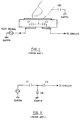
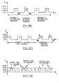
- FIG. 1 shows an example of a conventional capacitive coupled touch sensor according to the prior art.
- FIG. 2 shows the equivalent circuit of the sensor shown in FIG. 1.
- Plastic membrane switches are not suitable for applications where they are located close to high temperature sources, such as on a cooktop surface. When a plastic membrane is located in the vicinity of a heat source, it would have a tendency to warp or separate. They are also susceptible to easy damage by heat and abrasion in a situation where it is normal that objects are used nearby or can be placed on the membrane. Actuation of this type of switch is mechanical in nature and reliability is inherently reduced with use.
- Infra-red detection methods are sensitive to extraneous or even ambient light sources. Accumulation of foreign matter or objects placed over the sensing locations can affect sensitivity or produce erroneous detections. Moreover, the front plate or panel in front of the infra-red transmitters and detectors must be transparent for the technology to function.
- US-A-3 857 100 discloses an electronic switching arrangement having a touch contact, particularly for switching preselected channels in radio or television receivers.
- the alternating voltage which occurs across the contact when it is touched is rectified in a rectifier having such a long charge time constant that switching over is effected after a plurality of cycles of the alternating voltages.
- the object of the present invention is to provide a padless touch sensor employing direct capacitive coupling under a dielectric element, such as a glass window, a ceramic plate, etc.
- a dielectric element such as a glass window, a ceramic plate, etc.
- test pulses are sent to earth and when a user, standing by a sensor, touches the dielectric element at one sensing location, pulses are supplied to a conductive plate located under the dielectric element and in registry with the sensing location. These pulses are due to the capacitive reaction of the body of the user to the test pulses sent into earth. A coupling path is thus formed through the body capacitance with reference to earth.
- One of the important advantages of the present invention is that it is only the touch of the user that is actively coupling the circuit and activating the sensor, unlike the traditional sensing systems that depend on disturbing an existing capacitive circuit.
- the proposed touch sensor and method have several major impacts on overall system design. No conductive pads need to be deposited over the sensing location of the dielectric element for the system or method to function.
- the conductive plate of each sensor is instead provided in close contact with the opposite side of the dielectric element. This results in greater simplicity and flexibility with regards to the production and installation of a keyboard combining one or a plurality of sensors. Greater key density and a considerably smaller sensing location are possible compared to traditional capacitive sensing systems.
- the present invention features a padless touch sensor for detecting a touch at a sensing location onto a dielectric element by a user coupled to earth.
- the sensor comprises a conductive plate attached under the dielectric element and in registry with the sensing location.
- a means is provided for applying a predetermined potential on the conductive plate.
- Test pulses are injected into earth using a pulse test generating means and a means responsive to a potential variation in the conductive plate produces an output signal indicative of that variation.
- a potential variation occurs in the conductive plate during a test pulse due to a capacitive circuit formed between earth, the user and the means responsive to the potential variation.
- the present invention also provides a padless touch sensor for detecting a touch at sensing locations onto a dielectric element by a user coupled to earth.
- the sensor comprises a plurality of conductive plates, one for each sensing location. Each conductive plate is attached under the dielectric element and in registry with a respective sensing location. A predetermined potential is successively applied on one of the conductive plates at once. A test pulse is produced into earth while one of the conductive plates receives the predetermined potential. A means responsive to a potential variation in the conductive plate with the predetermined potential is then provided for producing an output signal indicative of the potential variation in that conductive plate.
- the present invention also provides a padless touch sensor for detecting a touch at sensing locations onto a dielectric element by a user coupled to earth.
- the sensor comprises a plurality of conductive plates, one for each sensing location. Each conductive plate is attached under the dielectric element and in registry with a respective sensing location.
- a means for applying a predetermined potential on the conductive plates is provided and test pulses are injected into earth.
- a means responsive to a potential variation in the conductive plates with the predetermined potential is then provided for producing output signals indicative of the potential variation in each of the conductive plates.
- a method for detecting a touch at a sensing location onto a dielectric element by a user coupled to earth comprises the steps of applying a predetermined potential on a conductive plate attached under the dielectric element and in registry with the sensing location. Test pulses are produced into earth and a potential variation on the conductive plate is sensed. An output signal indicative of the potential variation is then produced.
- a method for detecting a touch at sensing locations onto a dielectric element by a user coupled to earth Each sensing location is provided with a corresponding conductive plate attached under the dielectric element and in registry with the respective sensing location.
- the method comprises the steps of successively applying a predetermined potential on one of the conductive plates at once.
- a test pulse is produced into earth each time the predetermined potential is applied on one conductive plate.
- a potential variation in each of the conductive plates is sensed while the predetermined potential is applied thereon.
- An output signal is then produced. The output signal is indicative of the potential variation in each of the conductive plates while the predetermined potential is individually applied thereon.
- a method for detecting a touch at sensing locations onto a dielectric element by a user coupled to earth each sensing location being provided with a corresponding conductive plate attached under the dielectric element and in registry with the respective sensing location, the method comprising the steps of:
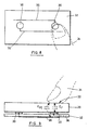
- the basic sensor (10) is mounted under a dielectric element (20) and is illustrated in a "touch" condition since the sensing location (22) on the dielectric element (20) is touched by a finger (24) of a user.
- the basic sensor (10) can be divided in two main parts, namely a test pulse generator section and a receiver section. Those parts are described in detail hereinbelow.
- the test pulse generator section produces test pulses into earth.
- the test pulse generating means comprises a resistor having an input terminal connected to a DC source and an output terminal connected to earth.
- the output terminal of the resistor is also connected to the collector of a transistor.
- the emitter of the transistor is then connected to the circuit ground.
- a pulsed signal is generated at the base of the transistor.
- FIGS. 3, 4 and 12 show such construction.
- a +24 volts DC potential is applied through a resistor R1 that is connected to earth.
- a typical value for the resistor R1 would be 10 Kohms.
- a transistor Q1 alternatively connects and disconnects the circuit ground to and from earth.
- a pulse signal V P of +5 volts for instance arrives at the base of the transistor Q1.
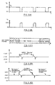
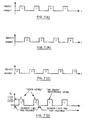
- FIGS. 5A and 5B respectively show the pulse signal V P and the resulting test pulse signal V t that is injected into earth.
- Earth in the context of the present invention means the real earth or any other mass acting as a virtual ground.
- the sensor can be connected to the real earth by means of a wire electrically connected to the grounding prong of the appliance, itself connected to the earth wire of the building.
- the virtual ground an example could be the metallic body of a vehicle.
- the receiver section of the basic sensor (10) comprises a conductive plate (30) located under the dielectric element (20).
- the plate (30) is in registry with the sensing location (22) onto the dielectric element (20).
- the sensing location (22) and the corresponding conductive plate (30) are also referred to as a "key". If appropriate, markings may be provided to indicate to the user the exact location where the finger (24) has to touch to achieve a touch condition at the key.
- markings may be provided to indicate to the user the exact location where the finger (24) has to touch to achieve a touch condition at the key.
- a person skilled in the art would realize that the term "finger” may be substituted for any body part that can be used for touching a key. For instance, a handicapped person may have to use his or her toes instead of one finger.
- the present invention may also work in applications where animals are involved.
- the receiver section further comprises a means for applying a predetermined potential on the plate (30). This sets a reference voltage, referred to as a "no touch" reference level. Then, a means responsive to a potential variation in the plate (30) is used to produce a signal indicative of the potential variation. It is this signal that will be used to determine if there is a touch condition or not.
- the plate (30) is attached under the dielectric element (20).
- the connection There are many ways of achieving the connection. One is to provide the plate (30) on a circuit board (32) and to connect the circuit board (32) with, for instance, an adhesive strip (34) or with screws (not shown). Of course, other kinds of attachments may be used, according to the particular needs and environment.
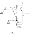
- FIG. 3 shows a possible embodiment of the present invention, where the means for applying a predetermined potential and the means responsive to a potential variation in the plate (30) are combined together using a transistor Q2.
- FIG. 4 shows the equivalent circuit when there is a touch condition, also referred to as a "key touch".
- the transistor Q2 is connected in a high input impedance emitter follower configuration.
- the voltage gain of the circuit is slightly less than 1.
- a resistor R b is connected between the base of the transistor Q2 and a second supply voltage source.
- the resistor R b serves as a termination and bias for the input and sets the "no touch" reference level at an output resistor R o .
- the other end of the resistor R o is connected to the circuit ground.
- a typical second supply voltage would be +5 volts DC.
- the input resistance R in at the base of the transistor Q2 is approximately given by the formula h FE x R o .
- the input resistance R in is then approximately between 0.5 Mohm and 2 Mohms for a typical transistor when the resistor R o is 4.7 Kohms and h FE between 100 and 400.
- Decreasing the value of the resistor R b raises the potential at the base of the transistor Q2 and also the "no touch" reference level. For instance, this level can be adjusted from +0.6 volt to +3.4 volts by adjusting the resistor R b from 5.6 Mohms to 200 Kohms.
- the detection level at the output resistor R o can also be adjusted by changing the value of the resistor R b to compensate for different coupling levels for various sizes of the conductive plates (30). Any convenient reference level can be chosen depending on the application and power supply voltage available.
- the V P test pulse signal drives the transistor Q1 which alternatively connects and disconnects the circuit ground to and from earth.
- the first supply voltage is +24 volts DC and when the transistor Q1 is switched off, the +24 volts DC is applied through the resistor R1 to earth for producing the test pulse signal V t .
- FIGS. 5A and 5B show the typical waveforms.
- the test pulse signal V t is applied once every 1 ms.
- the test pulse signal V t is coupled from earth to the capacitance CB of the body of the user.
- the potential at the conductive plate (30) will not change. Nevertheless, the est pulse V t is always being injected into ground and coupled to the user's body.
- the distance between the user and the test pulse generator section may be as far as 50 meters.
- a shielded cable was used to connect the plate (30) to the remote circuit board (32).
- the touch detection is achieved by coupling the +24 volts DC test pulse signal through the user's effective body capacitance, to the plate (30), by way of earth.
- the test pulse signal V t is applied to earth and to one side of body capacitance C B .
- the value of the capacitance C B is typically between 200 and 500 pF.
- the capacitance C B is connected in series to the capacitance C F , which represents the capacitance formed by the user's contact area at the sensing location (22), the dielectric element (20) and the conductive plate (30).
- a typical value of the capacitance C F is 20 pF for a 3 mm (1/8 inch) thick glass-ceramic with a dielectric constant of 22 and a plate area of about 3 mm 2 (0.5 square inch).
- a material with a higher relative dielectric constant increases the capacitance C F and produces improved signal coupling to the sensor or alternatively, allows the use of a thicker dielectric element (20).
- the area of the conductive plate (30) and the contact area of the finger (24) determines the value of the capacitance C F .
- Increasing the contact area will increase the capacitance and improve coupling of the test pulse signal V t to the sensor.
- the maximum area is however limited by the contact area for a typical human finger, beyond which increasing the area of the plate (30) has no effect.
- a circular plate of 13 mm (1/2 inch diameter) is a reasonable maximum useable limit to set for finger actuation.
- a 6 mm (1/4 inch) diameter plate works very reliably.
- the capacitance C B and C F acts instantly as a "short" and +24 volts would normally be applied to the base of the transistor Q2.
- the effective capacitance of C B and C F in the example is approximately 18 pF. Since the input base capacitance C in of the transistor Q2, which is in the range of 5 pF to 10 pF for a typical transistor, is comparable to the coupling capacitance of C B and C F combined, the signal level that the transistor Q2 receives is actually lower than +24 volts.
- the input resistance of the transistor Q2 also acts to reduce the level depending on the coupled resistance.
- the rise time of the test pulse signal V t also acts to further reduce this level.
- the coupled signal level is further reduced.
- the transmitted test pulse signal V t from earth generally does not have a very sharp rise time.
- the effective signal coupled to the transistor Q2 is thus much lower than +24 volts, and typically is ⁇ 0.3 volt.
- FIG. 5C shows an example of a key touch period with reference to the test pulse signal V t shown in FIG. 5B.
- FIG. 5D then shows the resulting variation of the potential in the plate (30).
- FIG. 5E shows how the potential variation is felt at the emitter of the transistor Q2.
- the output signal V o is sent to an appropriate device to determine whether or not the potential variation is sufficient to initiate a positive key touch status and, for instance, actuate a corresponding switch (not shown).
- FIG. 6 shows a multiple key configuration.
- the keys are each individually scanned to determine whether there is a key touch or not.
- the input to the base of the selected key transistor is left active (enabled) while the inputs to the other keys are disabled by grounding their input bases through a multiplexer.
- the individual key transistor Q2 and resistance R b are called a "selector".
- FIGS. 7A, 7B and 7C illustrate schematically the selection of the individual keys.
- the test pulse signal is coupled to that key only if there is a touch at the corresponding sensing location. It should be noted that the test pulse generator section was omitted from FIG. 6 for simplification.
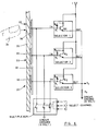
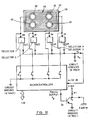
- FIG. 12 shows the complete system with "N" keys.
- FIG. 7D shows an example of the input voltage V i for the first key.
- the first key is touched in the first two readings of that key, while there is no key touch for the other two readings.
- FIG. 7E shows the input voltage V i for the second key, showing the signal if only the second key is touched during the second reading.
- FIG. 7F shows the output voltage V i for the third key, showing the signal if only the third key is touched during the last two readings.
- FIG. 7G shows the resulting output signal V o in function of time. It should be noted that any stray or inadvertent coupling to any of the other disabled keys has no effect on the output voltage V o at the resistor R o for the time period that the first key is selected, for instance. Only the first key contributes to the voltage V o for that time period. Every other key is then subsequently scanned in a similar manner with the voltage level present at a common output resistor R o , indicative of the presence of a key touch for that particular key. When there is no key touch, the output signal V o remains at its reference no touch level for the scanned key. It should be noted at this point that it is possible to provide an output resistor R o for each key.
- One of the advantages of the present invention is that no deposition of conductive films on the dielectric element (20) or other special processes are required.
- the dielectric element (20) not only protects the sensor from the external operating environment, it acts in completing the capacitance construction of C F .
- the only conductive plates contributing to the coupling capacitance are behind the dielectric element (20) and are then protected from the action of chemicals and abrasion.
- the circuit board (32) does not have the same tendency to warp or distort like the conventional plastic membrane switch type construction. Moreover, foreign matter or objects placed directly on top of the dielectric element (20) will not erroneously actuate any of the keys. Infra-red based systems do not preclude this possibility.
- a circuit ground plane Surrounding the sensing locations (22) on the outward facing or user side of the circuit board (32) by a circuit ground plane (40), as shown in FIGS. 10 and 11, has the effect of shielding all conductive traces behind it.
- a key touch at a sensing location (22) which also overlaps another trace now has its capacitance C FC to the overlapped trace (36) coupled to circuit ground.
- C FC capacitance
- FIG. 12 illustrates conductive plates (30) and circuit ground plane (40) that are etched on the outward facing side of a circuit board (32).
- a dielectric element (20) covers and is in close contact with the keys.
- the outputs of all the corresponding selectors are connected to a common output resistor R o .
- R o common output resistor
- a microcontroller provides the necessary signals for scanning the selector of each key of the array. Measurement and analysis of the potential variations at the output resistor R o is performed by the microcontroller. A determination of whether a valid key touch has been received and the appropriate reaction is then performed.
- the keys in FIG. 12 are scanned in succession, in an order prescribed by the microcontroller program.
- the microcontroller sends a pulse to the transistor Q1.
- the transistor Q1 raises earth potential to +24 volts above circuit ground when the input pulse V P is zero Volt.
- the microcontroller disables all the other keys. This may be done by grounding every transistor base of the selectors except the one that it is scanning if one output resistor R o is used.
- the output voltage V o is connected to the A/D input channel of the microcontroller which is read and recorded in memory.
- the microcontroller then enables the next key and disables all the others and proceeds in the same manner as previously described until all the keys have been scanned.
- the microcontroller then suspends the scanning in order to evaluate the potential levels for V o detected during each key scan period.
- the microcontroller initially records the "no key touch" reference level V o for each key.
- the current recorded V o level for a particular key is then compared with the reference "no key touch” value. If the potential V o is greater than the reference by a predetermined reference value, then a "possible key touch" is recognized as to have occurred. This "difference level" represents the detection level range for the key.
- the recorded "no key touch” reference level in memory for the respective keys will be adjusted to a new value such that the potential variation calculated by the microcontroller will always be less than the "possible key touch” detection range. Those keys will thus be forced to be seen as “not touched” and be effectively locked out. The scanning of the keys then proceeds normally. When the multiple touch condition disappears, the "no touch" reference levels for those keys are returned to their normal values in memory.
- the microcontroller is provided with a proper program to perform the steps of the method according to the present invention.
- An example of such a program is as follows. This program was written for a sensor used in conjunction with an electric range having a ceramic cooktop surface.
Landscapes
- Engineering & Computer Science (AREA)
- General Engineering & Computer Science (AREA)
- Theoretical Computer Science (AREA)
- Human Computer Interaction (AREA)
- Physics & Mathematics (AREA)
- General Physics & Mathematics (AREA)
- Electronic Switches (AREA)
- Switches That Are Operated By Magnetic Or Electric Fields (AREA)
Description
- Conventional capacitive touch sensing systems employ a passive form of detection. In such sensor, there is an existing capacitive circuit driven by a source signal. A key touch, representing a change to the circuit capacitance, results in attenuating the potential and resulting voltage level change indicates a key touch. This capacitive circuit is usually implemented by the deposition of opposing conductive key pads to opposite sides of a dielectric element.
- FIG. 1 shows an example of a conventional capacitive coupled touch sensor according to the prior art. FIG. 2 shows the equivalent circuit of the sensor shown in FIG. 1.
- One problem with conventional sensors is that accumulation of foreign deposits on the key pads has the drawback of negating the effect of a touch by the user. Chemicals and abrasion of the exposed key pads can also degrade performance. Yet, different dielectric characteristics, such as thickness and dielectric constant, result in having to change or redesign the size of the key pads to achieve the same capacitance for a different dielectric element in identical applications.
- Another type of conventional sensing system is a plastic membrane switch. Plastic membrane switches are not suitable for applications where they are located close to high temperature sources, such as on a cooktop surface. When a plastic membrane is located in the vicinity of a heat source, it would have a tendency to warp or separate. They are also susceptible to easy damage by heat and abrasion in a situation where it is normal that objects are used nearby or can be placed on the membrane. Actuation of this type of switch is mechanical in nature and reliability is inherently reduced with use.
- Infra-red detection methods are sensitive to extraneous or even ambient light sources. Accumulation of foreign matter or objects placed over the sensing locations can affect sensitivity or produce erroneous detections. Moreover, the front plate or panel in front of the infra-red transmitters and detectors must be transparent for the technology to function.
- US-A-3 857 100 discloses an electronic switching arrangement having a touch contact, particularly for switching preselected channels in radio or television receivers. The alternating voltage which occurs across the contact when it is touched is rectified in a rectifier having such a long charge time constant that switching over is effected after a plurality of cycles of the alternating voltages.
- The object of the present invention is to provide a padless touch sensor employing direct capacitive coupling under a dielectric element, such as a glass window, a ceramic plate, etc. This sensor and the corresponding method have several important advantages over the traditional touch sensing systems and methods previously described.
- According to the present invention, test pulses are sent to earth and when a user, standing by a sensor, touches the dielectric element at one sensing location, pulses are supplied to a conductive plate located under the dielectric element and in registry with the sensing location. These pulses are due to the capacitive reaction of the body of the user to the test pulses sent into earth. A coupling path is thus formed through the body capacitance with reference to earth.
- One of the important advantages of the present invention is that it is only the touch of the user that is actively coupling the circuit and activating the sensor, unlike the traditional sensing systems that depend on disturbing an existing capacitive circuit.
- The proposed touch sensor and method have several major impacts on overall system design. No conductive pads need to be deposited over the sensing location of the dielectric element for the system or method to function. The conductive plate of each sensor is instead provided in close contact with the opposite side of the dielectric element. This results in greater simplicity and flexibility with regards to the production and installation of a keyboard combining one or a plurality of sensors. Greater key density and a considerably smaller sensing location are possible compared to traditional capacitive sensing systems.
- In particular, the present invention features a padless touch sensor for detecting a touch at a sensing location onto a dielectric element by a user coupled to earth. The sensor comprises a conductive plate attached under the dielectric element and in registry with the sensing location. A means is provided for applying a predetermined potential on the conductive plate. Test pulses are injected into earth using a pulse test generating means and a means responsive to a potential variation in the conductive plate produces an output signal indicative of that variation. In use, when the user touches the dielectric element at the sensing location, a potential variation occurs in the conductive plate during a test pulse due to a capacitive circuit formed between earth, the user and the means responsive to the potential variation.
- The present invention also provides a padless touch sensor for detecting a touch at sensing locations onto a dielectric element by a user coupled to earth. The sensor comprises a plurality of conductive plates, one for each sensing location. Each conductive plate is attached under the dielectric element and in registry with a respective sensing location. A predetermined potential is successively applied on one of the conductive plates at once. A test pulse is produced into earth while one of the conductive plates receives the predetermined potential. A means responsive to a potential variation in the conductive plate with the predetermined potential is then provided for producing an output signal indicative of the potential variation in that conductive plate.
- The present invention also provides a padless touch sensor for detecting a touch at sensing locations onto a dielectric element by a user coupled to earth. The sensor comprises a plurality of conductive plates, one for each sensing location. Each conductive plate is attached under the dielectric element and in registry with a respective sensing location. A means for applying a predetermined potential on the conductive plates is provided and test pulses are injected into earth. A means responsive to a potential variation in the conductive plates with the predetermined potential is then provided for producing output signals indicative of the potential variation in each of the conductive plates.
- According to the present invention, there is also provided a method for detecting a touch at a sensing location onto a dielectric element by a user coupled to earth. The method comprises the steps of applying a predetermined potential on a conductive plate attached under the dielectric element and in registry with the sensing location. Test pulses are produced into earth and a potential variation on the conductive plate is sensed. An output signal indicative of the potential variation is then produced.
- According to another aspect of the present invention, there is also provided a method for detecting a touch at sensing locations onto a dielectric element by a user coupled to earth. Each sensing location is provided with a corresponding conductive plate attached under the dielectric element and in registry with the respective sensing location. The method comprises the steps of successively applying a predetermined potential on one of the conductive plates at once. A test pulse is produced into earth each time the predetermined potential is applied on one conductive plate. A potential variation in each of the conductive plates is sensed while the predetermined potential is applied thereon. An output signal is then produced. The output signal is indicative of the potential variation in each of the conductive plates while the predetermined potential is individually applied thereon.
- According to another aspect of the present invention, there is provided a method for detecting a touch at sensing locations onto a dielectric element by a user coupled to earth, each sensing location being provided with a corresponding conductive plate attached under the dielectric element and in registry with the respective sensing location, the method comprising the steps of:
- applying a predetermined potential on the conductive plates;
- producing test pulses into earth;
- sensing a potential variation in each of the conductive plates; and
- producing output signals indicative of the potential variation in each of the conductive plates while they are being sensed.
-
- A non restrictive description of preferred embodiments will now be given with reference to the appended drawings.
-
- FIG. 1
- is a schematic view of a capacitive coupled touch sensor according to the prior art.
- FIG. 2
- is a schematic circuit diagram of the equivalent circuit of the sensor shown in FIG. 1.
- FIG. 3
- is a schematic view of a basic padless touch sensor according to a possible embodiment of the present invention.
- FIG. 4
- is a schematic circuit diagram of the equivalent circuit of the basic sensor shown in FIG. 3.
- FIG. 5A
- is a graph showing an example of the pulse signal VP in function of time in the sensor of FIG. 3.
- FIG. 5B
- is a graph showing an example of the pulse test signal Vt in function of time in the sensor of FIG. 3.
- FIG. 5C
- is a schematic representation of an example of a key touch scenario in function of time.
- FIG. 5D
- is a graph showing an example of the input signal Vi representing the potential of the conductive plate in function of time in the sensor of FIG. 3 and during the key touch scenario of FIG. 5C.
- FIG. 5E
- is a graph showing an example of the output signal Vo representing the potential at the output of the transistor Q2 in function of time in the sensor of FIG. 3 and in response to the input signal Vi shown in FIG. 5D.
- FIG. 6
- is a schematic view of a padless touch sensor with multiple keys, according to a preferred embodiment of the present invention, shown without the test pulse signal generator.
- FIG. 7A
- is a schematic representation in function of time of the selection of the first key of FIG. 6.
- FIG. 7B
- is a schematic representation in function of time of the selection of the second key of FIG. 6.
- FIG. 7C
- is a schematic representation in function of time of the selection of the third key of FIG. 6.
- FIG. 7D
- is a graph showing an example of the input signal Vi representing the potential of the conductive plate of the first key of FIG. 6 in function of time and following the key selection shown in FIG. 7A.
- FIG. 7E
- is a graph showing an example of the input signal Vi representing the potential of the conductive plate of the second key of FIG. 6 in function of time and following the key selection shown in FIG. 7B.
- FIG. 7F
- is a graph showing an example of the input signal Vi representing the potential of the conductive plate of the third key of FIG. 6 in function of time and following the key selection shown in FIG. 7C.
- FIG. 7G
- is a graph showing an example of the resulting output signal Vo representing the potential at the output of the transistor Q2 in function of time in the sensor of FIG. 6 and in response to the input signals Vi shown in FIGS. 7D, 7E and 7F.
- FIG. 8
- is a schematic view of an example of a touch at a sensing location which overlaps different traces.
- FIG. 9
- is a schematic circuit diagram of the equivalent circuit of the sensor shown in FIG. 8.
- FIG. 10
- is a schematic view of an example of a sensor with a grounding plate.
- FIG. 11
- is a schematic circuit diagram of the equivalent circuit of the sensor shown in FIG. 10.
- FIG. 12
- is a schematic view of a sensor with multiple keys, according to a preferred embodiment of the present invention.
- Referring to FIG. 3, there is shown a basic sensor (10) according to a possible embodiment of the present invention. The basic sensor (10) is mounted under a dielectric element (20) and is illustrated in a "touch" condition since the sensing location (22) on the dielectric element (20) is touched by a finger (24) of a user.
- The basic sensor (10) can be divided in two main parts, namely a test pulse generator section and a receiver section. Those parts are described in detail hereinbelow.
- The test pulse generator section produces test pulses into earth. Preferably, the test pulse generating means comprises a resistor having an input terminal connected to a DC source and an output terminal connected to earth. The output terminal of the resistor is also connected to the collector of a transistor. The emitter of the transistor is then connected to the circuit ground. A pulsed signal is generated at the base of the transistor. FIGS. 3, 4 and 12 show such construction. In this embodiment, a +24 volts DC potential is applied through a resistor R1 that is connected to earth. A typical value for the resistor R1 would be 10 Kohms. A transistor Q1 alternatively connects and disconnects the circuit ground to and from earth. A pulse signal VP of +5 volts for instance, arrives at the base of the transistor Q1. The circuit ground and earth are disconnected whenever VP drops to 0 volt. This applies a +24 volts, with reference to the circuit ground, at the opposite side of the resistor R1. As soon as the pulse signal VP is back to the +5 volt level, the transistor Q1 is switched on again and the circuit ground and earth are connected together, dropping Vt to 0 volt. FIGS. 5A and 5B respectively show the pulse signal VP and the resulting test pulse signal Vt that is injected into earth.
- Earth in the context of the present invention means the real earth or any other mass acting as a virtual ground. For instance, in case of an appliance, the sensor can be connected to the real earth by means of a wire electrically connected to the grounding prong of the appliance, itself connected to the earth wire of the building. As for the virtual ground, an example could be the metallic body of a vehicle.
- The receiver section of the basic sensor (10) comprises a conductive plate (30) located under the dielectric element (20). The plate (30) is in registry with the sensing location (22) onto the dielectric element (20). The sensing location (22) and the corresponding conductive plate (30) are also referred to as a "key". If appropriate, markings may be provided to indicate to the user the exact location where the finger (24) has to touch to achieve a touch condition at the key. Of course, a person skilled in the art would realize that the term "finger" may be substituted for any body part that can be used for touching a key. For instance, a handicapped person may have to use his or her toes instead of one finger. The present invention may also work in applications where animals are involved.
- The receiver section further comprises a means for applying a predetermined potential on the plate (30). This sets a reference voltage, referred to as a "no touch" reference level. Then, a means responsive to a potential variation in the plate (30) is used to produce a signal indicative of the potential variation. It is this signal that will be used to determine if there is a touch condition or not.
- As aforesaid, the plate (30) is attached under the dielectric element (20). There are many ways of achieving the connection. One is to provide the plate (30) on a circuit board (32) and to connect the circuit board (32) with, for instance, an adhesive strip (34) or with screws (not shown). Of course, other kinds of attachments may be used, according to the particular needs and environment.
- FIG. 3 shows a possible embodiment of the present invention, where the means for applying a predetermined potential and the means responsive to a potential variation in the plate (30) are combined together using a transistor Q2. FIG. 4 shows the equivalent circuit when there is a touch condition, also referred to as a "key touch".
- The transistor Q2 is connected in a high input impedance emitter follower configuration. The voltage gain of the circuit is slightly less than 1. A resistor Rb is connected between the base of the transistor Q2 and a second supply voltage source. The resistor Rb serves as a termination and bias for the input and sets the "no touch" reference level at an output resistor Ro. The other end of the resistor Ro is connected to the circuit ground.
- A typical second supply voltage would be +5 volts DC. The input resistance Rin at the base of the transistor Q2 is approximately given by the formula hFE x Ro. The input resistance Rin is then approximately between 0.5 Mohm and 2 Mohms for a typical transistor when the resistor Ro is 4.7 Kohms and hFE between 100 and 400. Decreasing the value of the resistor Rb raises the potential at the base of the transistor Q2 and also the "no touch" reference level. For instance, this level can be adjusted from +0.6 volt to +3.4 volts by adjusting the resistor Rb from 5.6 Mohms to 200 Kohms. The detection level at the output resistor Ro can also be adjusted by changing the value of the resistor Rb to compensate for different coupling levels for various sizes of the conductive plates (30). Any convenient reference level can be chosen depending on the application and power supply voltage available.
- In use, the VP test pulse signal drives the transistor Q1 which alternatively connects and disconnects the circuit ground to and from earth. In the illustrated embodiment, the first supply voltage is +24 volts DC and when the transistor Q1 is switched off, the +24 volts DC is applied through the resistor R1 to earth for producing the test pulse signal Vt. FIGS. 5A and 5B show the typical waveforms. Preferably, the test pulse signal Vt is applied once every 1 ms.
- The test pulse signal Vt is coupled from earth to the capacitance CB of the body of the user. When there is no key touch, the potential at the conductive plate (30) will not change. Nevertheless, the est pulse Vt is always being injected into ground and coupled to the user's body. Experiments have shown that the distance between the user and the test pulse generator section may be as far as 50 meters. A shielded cable was used to connect the plate (30) to the remote circuit board (32).
- When there is a key touch, like in FIGS. 3 and 4, the touch detection is achieved by coupling the +24 volts DC test pulse signal through the user's effective body capacitance, to the plate (30), by way of earth. The test pulse signal Vt is applied to earth and to one side of body capacitance CB. The value of the capacitance CB is typically between 200 and 500 pF. During a key touch, the capacitance CB is connected in series to the capacitance CF, which represents the capacitance formed by the user's contact area at the sensing location (22), the dielectric element (20) and the conductive plate (30). A typical value of the capacitance CF is 20 pF for a 3 mm (1/8 inch) thick glass-ceramic with a dielectric constant of 22 and a plate area of about 3 mm2 (0.5 square inch). A material with a higher relative dielectric constant increases the capacitance CF and produces improved signal coupling to the sensor or alternatively, allows the use of a thicker dielectric element (20). Increasing the thickness of the dielectric element (20), with the area of the plate (30) remaining constant, decreases the value of CF and the resulting coupling to the sensor.
- The capacitance for parallel plates is given by the following general formula:
- A is the area of plates,
- d is the distance between the plates,
- e is a constant, and
- k is the relative dielectric constant.
-
- One can see that for a dielectric element of a specific thickness, the area of the conductive plate (30) and the contact area of the finger (24) determines the value of the capacitance CF. Increasing the contact area will increase the capacitance and improve coupling of the test pulse signal Vt to the sensor. The maximum area is however limited by the contact area for a typical human finger, beyond which increasing the area of the plate (30) has no effect. A circular plate of 13 mm (1/2 inch diameter) is a reasonable maximum useable limit to set for finger actuation. However, a 6 mm (1/4 inch) diameter plate works very reliably.
- When the test pulse signal Vt goes from 0 volt to +24 volts, the capacitance CB and CF acts instantly as a "short" and +24 volts would normally be applied to the base of the transistor Q2. The effective capacitance of CB and CF in the example is approximately 18 pF. Since the input base capacitance Cin of the transistor Q2, which is in the range of 5 pF to 10 pF for a typical transistor, is comparable to the coupling capacitance of CB and CF combined, the signal level that the transistor Q2 receives is actually lower than +24 volts. The input resistance of the transistor Q2 also acts to reduce the level depending on the coupled resistance. The rise time of the test pulse signal Vt also acts to further reduce this level. If this time is comparable or greater than the time constant of the input resistance of the transistor Q2 and the coupling capacitance (CB and CF), the coupled signal level is further reduced. The transmitted test pulse signal Vt from earth generally does not have a very sharp rise time. The effective signal coupled to the transistor Q2 is thus much lower than +24 volts, and typically is ±0.3 volt.
- FIG. 5C shows an example of a key touch period with reference to the test pulse signal Vt shown in FIG. 5B. FIG. 5D then shows the resulting variation of the potential in the plate (30). FIG. 5E shows how the potential variation is felt at the emitter of the transistor Q2. The output signal Vo is sent to an appropriate device to determine whether or not the potential variation is sufficient to initiate a positive key touch status and, for instance, actuate a corresponding switch (not shown).
- FIG. 6 shows a multiple key configuration. The keys are each individually scanned to determine whether there is a key touch or not. The input to the base of the selected key transistor is left active (enabled) while the inputs to the other keys are disabled by grounding their input bases through a multiplexer. The individual key transistor Q2 and resistance Rb are called a "selector".
- FIGS. 7A, 7B and 7C illustrate schematically the selection of the individual keys. When a key is selected, the test pulse signal is coupled to that key only if there is a touch at the corresponding sensing location. It should be noted that the test pulse generator section was omitted from FIG. 6 for simplification. FIG. 12 shows the complete system with "N" keys.
- FIG. 7D shows an example of the input voltage Vi for the first key. In the given example, the first key is touched in the first two readings of that key, while there is no key touch for the other two readings. FIG. 7E shows the input voltage Vi for the second key, showing the signal if only the second key is touched during the second reading. FIG. 7F shows the output voltage Vi for the third key, showing the signal if only the third key is touched during the last two readings.
- FIG. 7G shows the resulting output signal Vo in function of time. It should be noted that any stray or inadvertent coupling to any of the other disabled keys has no effect on the output voltage Vo at the resistor Ro for the time period that the first key is selected, for instance. Only the first key contributes to the voltage Vo for that time period. Every other key is then subsequently scanned in a similar manner with the voltage level present at a common output resistor Ro, indicative of the presence of a key touch for that particular key. When there is no key touch, the output signal Vo remains at its reference no touch level for the scanned key. It should be noted at this point that it is possible to provide an output resistor Ro for each key.
- One of the advantages of the present invention is that no deposition of conductive films on the dielectric element (20) or other special processes are required. The dielectric element (20) not only protects the sensor from the external operating environment, it acts in completing the capacitance construction of CF. The only conductive plates contributing to the coupling capacitance are behind the dielectric element (20) and are then protected from the action of chemicals and abrasion.
- Heat sensitivity is not an issue. For instance, the circuit board (32) does not have the same tendency to warp or distort like the conventional plastic membrane switch type construction. Moreover, foreign matter or objects placed directly on top of the dielectric element (20) will not erroneously actuate any of the keys. Infra-red based systems do not preclude this possibility.
- As with traditional capacitive touch sensing systems, special considerations must be taken into account in designing the circuit board (32). As shown in FIG. 8, when a conductive trace (36) connected to a conductive plate (30) runs close to another plate (30), a key touch at a certain sensing location (22) may overlap a different sensor trace (36). The dielectric capacitance CF from the user to the overlapped adjacent trace could couple some of the signal Vi to the corresponding key (CFC), as shown in FIG. 9. Efforts to reduce this effect as much as possible result in improved determination of a key touch. This effect is minimized by making the traces (36) as thin as possible, thus reducing undesired capacitive coupling. Surrounding the sensing locations (22) on the outward facing or user side of the circuit board (32) by a circuit ground plane (40), as shown in FIGS. 10 and 11, has the effect of shielding all conductive traces behind it. A key touch at a sensing location (22) which also overlaps another trace now has its capacitance CFC to the overlapped trace (36) coupled to circuit ground. Furthermore, a minimum number of conductive traces (36) should run on the outward facing side of the keyboard to be able to make effective use of the shielding.
- FIG. 12 illustrates conductive plates (30) and circuit ground plane (40) that are etched on the outward facing side of a circuit board (32). A dielectric element (20) covers and is in close contact with the keys. The outputs of all the corresponding selectors are connected to a common output resistor Ro. As aforesaid, it is possible to provide a separate output resistor Ro for each key. This would however require more than one output channel. A microcontroller provides the necessary signals for scanning the selector of each key of the array. Measurement and analysis of the potential variations at the output resistor Ro is performed by the microcontroller. A determination of whether a valid key touch has been received and the appropriate reaction is then performed.
- In use, the keys in FIG. 12 are scanned in succession, in an order prescribed by the microcontroller program. At the beginning of the process, the microcontroller sends a pulse to the transistor Q1. The transistor Q1 raises earth potential to +24 volts above circuit ground when the input pulse VP is zero Volt. When a particular key is scanned, the microcontroller disables all the other keys. This may be done by grounding every transistor base of the selectors except the one that it is scanning if one output resistor Ro is used.
- The output voltage Vo is connected to the A/D input channel of the microcontroller which is read and recorded in memory. The microcontroller then enables the next key and disables all the others and proceeds in the same manner as previously described until all the keys have been scanned. The microcontroller then suspends the scanning in order to evaluate the potential levels for Vo detected during each key scan period. The microcontroller initially records the "no key touch" reference level Vo for each key. The current recorded Vo level for a particular key is then compared with the reference "no key touch" value. If the potential Vo is greater than the reference by a predetermined reference value, then a "possible key touch" is recognized as to have occurred. This "difference level" represents the detection level range for the key. The potential variations for a possible "key touch" for each of the other keys during their scan period are similarly generated. The key which has the largest potential variation is then recognized as being "most probably" touched. This sequence of events is performed several times. When a particular key consistently produces the largest potential variation, the corresponding key is accepted as being "touched". Typically a difference level of +0.2 volt produces acceptable results.
- When the microcontroller encounters a multiple "key touch" situation, the recorded "no key touch" reference level in memory for the respective keys will be adjusted to a new value such that the potential variation calculated by the microcontroller will always be less than the "possible key touch" detection range. Those keys will thus be forced to be seen as "not touched" and be effectively locked out. The scanning of the keys then proceeds normally. When the multiple touch condition disappears, the "no touch" reference levels for those keys are returned to their normal values in memory.
- The microcontroller is provided with a proper program to perform the steps of the method according to the present invention. An example of such a program is as follows. This program was written for a sensor used in conjunction with an electric range having a ceramic cooktop surface.
Claims (17)
- A padless touch sensor (10) for detecting a touch at a sensing location (22) by a user (24) coupled to earth, the sensor (10) being characterized in that it comprises :whereby, when the user (24) touches the dielectric element (20) at the sensing location (22), a potential variation occurs in the conductive plate (30) during a test pulse (Vt) due to a capacitive circuit formed between earth, the user (24) and the means responsive to the potential variation.a dielectric element (20);a conductive plate (30);a means for attaching the conductive plate (30) under the dielectric element (20) and in registry with the sensing location (22);a means for applying a predetermined potential on the conductive plate (30);a test pulse (Vt) generating means for producing test pulses (Vt) into earth; anda means responsive to a potential variation in the conductive plate (30) for producing an output signal (VO) indicative of the potential variation;
- A padless touch sensor (10) according to claim 1, the test pulse generating means comprising :a resistor (R1) having an input terminal and an output terminal,the input terminal being connected to a DC source and the output terminal being connected to earth,a transistor (Q1) having a collector, an emitter and a base, the collector being connected to the output terminal of the resistor (R1) and the emitter being connected to circuit ground; anda means for generating a pulsed signal (VP) at the base of the transistor (Q1).
- A padless touch sensor (10) according to claim 1 or 2, the means for applying a predetermined potential and the means responsive to a potential variation comprising :whereby the output signal (VO) is read at the input terminal of the second resistor (RO).a first resistor (Rb) having an input terminal and an output terminal, the input terminal of the first resistor (Rb) being connected to a DC source and the output terminal of the first resistor (Rb) being connected to the conductive plate (30),a transistor (Q2) having a collector, an emitter and a base, the collector being connected to the DC source and the base being connected to the conductive plate (30) and to the output terminal of the first resistor (Rb); anda second resistor (RO) having an input terminal and an output terminal, the input terminal of the second resistor (RO) being connected to the emitter of the transistor and the output terminal of the second resistor (RO) being connected to circuit ground;
- A padless touch sensor (10) for detecting a touch at sensing locations (22) by a user (24) coupled to earth, the sensor (10) being characterized in that it comprises :whereby, when the user (24) touches the dielectric element (20) at one of the sensing locations (22), a potential variation occurs in the conductive plate (30) during a test pulse (Vt) due to a capacitive circuit formed between earth, the user (24) and the means responsive to the potential variation.a dielectric element (20);a plurality of conductive plates (30), one for each sensing location (22);a means for attaching each conductive plate (30) under the dielectric element (20) and in registry with a respective sensing location (22);a means for successively applying a predetermined potential on one of the conductive plates (30) at once;a test pulse generating means for producing a test pulse (Vt) into earth while one of the conductive plates (30) receives the predetermined potential; anda means responsive to a potential variation in the conductive plate (30) with the predetermined potential for producing an output signal (VO) indicative of the potential variation in that conductive plate (30);
- A padless touch sensor (10) according to claim 4, the test pulse generating means comprising :a resistor (R1) having an input terminal and an output terminal, the input terminal being connected to a DC source and the output terminal being connected to earth,a transistor (Q1) having a collector, an emitter and a base, the collector being connected to the output terminal of the resistor (R1) and the emitter being connected to circuit ground; anda means for generating a pulsed signal (VP) at the base of the transistor (Q1).
- A padless touch sensor (10) according to claim 4 or 5, the means for applying a predetermined potential and the means responsive to a potential variation comprising :whereby the output signal (VO) is read at the input terminal of the second resistor (RO).a plurality of first resistors (Rb), each having an input terminal and an output terminal, the input terminal of each first resistor (Rb) being connected to a DC source and the output terminal of each first resistor (Rb) being connected to a respective conductive plate (30);a plurality of transistors (Q2), each having a collector, an emitter and a base, the collector of each transistor (Q2) being connected to the DC source and the base of each transistor (Q2) being connected to a respective conductive plate (30) and to the output terminal of the respective first resistor (Rb);a second resistor (RO) having an input terminal and an output terminal, the input terminal of the second resistor (RO) being connected to the emitter of each transistor (Q2) and the output terminal of the second resistor (RO) being connected to circuit ground; anda means for selectively connecting the conductive plates (30) to the circuit ground except the one with the predetermined potential;
- A padless touch sensor (10) according to claim 4, 5 or 6, further comprising a circuit ground plane (40) surrounding the sensing locations (22) to shield conductive traces (36) originating from the conductive plates (30).
- A padless touch sensor (10) for detecting a touch at sensing locations (22). by a user (24) coupled to earth, the sensor (10) being characterized in that it comprises :whereby, when the user (24) touches the dielectric element (20) at one of the sensing locations (22), a potential variation occurs in the corresponding conductive plate (30) during a test pulse (Vt) due to a capacitive circuit formed between earth, the user (24) and the means responsive to the potential variation.a dielectric element (20);a plurality of conductive plates (30), one for each sensing location (22);a means for attaching each conductive plate (30) under the dielectric element (20) and in registry with a respective sensing location (22);a means for applying a predetermined potential on the conductive plates (30);a test pulse generating means for producing test pulses (Vt) into earth; anda means responsive to a potential variation in the conductive plates (30) with the predetermined potential for producing output signals (VO) indicative of the potential variation in each of the conductive plates (30);
- A padless touch sensor (10) according to claim 8, the test pulse generating means comprising :a resistor (R1) having an input terminal and an output terminal, the input terminal being connected to a DC source and the output terminal being connected to earth,a transistor (Q1) having a collector, an emitter and a base, the collector being connected to the output terminal of the resistor (R1) and the emitter being connected to circuit ground; anda means for generating a pulsed signal (VP) at the base of the transistor (Q1).
- A padless touch sensor (10) according to claim 8 or 9, further comprising a circuit ground plane (40) surrounding the sensing locations (22) to shield conductive traces (36) originating from the conductive plates (30).
- A method for detecting a touch at a sensing location (22) onto a dielectric element (20) by a user (24) coupled to earth, comprising the steps of:applying a predetermined potential on a conductive plate (30) attached under the dielectric element (20) and in registry with the sensing location (22);producing test pulses (Vt) into earth;sensing a potential variation on the conductive plate (30); andproducing an output signal (VO) indicative of the potential variation.
- A method for detecting a touch according to claim 11, further comprising the steps of:comparing the output signal (VO) to a reference level; andproducing a signal indicative of a touch at the sensing location (22) when the potential variation on the conductive plate (30) is greater than the reference level.
- A method for detecting a touch at sensing locations (22) onto a dielectric element (20) by a user (24) coupled to earth, each sensing location (22) being provided with a corresponding conductive plate (30) attached under the dielectric element (20) and in registry with the respective sensing location (22), said method comprising the steps of:successively applying a predetermined potential on one of the conductive plates (30) at once;producing a test pulse (Vt) into earth while the predetermined potential is applied on one conductive plate (30);sensing a potential variation in each of the conductive plates (30) while the predetermined potential is applied thereon; andproducing an output signal (VO) indicative of the potential variation in each of the conductive plates (30) while the predetermined potential is individually applied thereon.
- A method for detecting a touch according to claim 13, the step of successively applying a predetermined potential on one of the conductive plates (30) at once comprising connecting the conductive plates (30) to circuit ground except the one with the predetermined potential.
- A method for detecting a touch according to claim 13 or 14, further comprising the steps of:comparing the output signal (VO) to a reference level; andproducing a signal indicative of a touch at one of the sensing locations (22) when the potential variation on the corresponding conductive plate (30) is greater than the reference level.
- A method for detecting a touch at sensing locations (22) onto a dielectric element (20) by a user (24) coupled to earth, each sensing location (22) being provided with a corresponding conductive plate (30) attached under the dielectric element (20) and in registry with the respective sensing location (22), said method comprising the steps of:applying a predetermined potential on the conductive plates (30);producing test pulses (Vt) into earth;sensing a potential variation in each of the conductive plates (30); andproducing output signals (VO) indicative of the potential variation in each of the conductive plates (30) while they are being sensed.
- A method for detecting a touch according to claim 16, further comprising the steps of:comparing the output signals (VO) to a reference level; andproducing a signal indicative of a touch at one of the sensing locations (22) when the potential variation on the corresponding conductive plate (30) is greater than the reference level.
Applications Claiming Priority (2)
| Application Number | Priority Date | Filing Date | Title |
|---|---|---|---|
| US1463896P | 1996-04-15 | 1996-04-15 | |
| US14638 | 1996-04-15 |
Publications (3)
| Publication Number | Publication Date |
|---|---|
| EP0802500A2 EP0802500A2 (en) | 1997-10-22 |
| EP0802500A3 EP0802500A3 (en) | 1998-10-07 |
| EP0802500B1 true EP0802500B1 (en) | 1999-08-18 |
Family
ID=21766735
Family Applications (1)
| Application Number | Title | Priority Date | Filing Date |
|---|---|---|---|
| EP97400846A Expired - Lifetime EP0802500B1 (en) | 1996-04-15 | 1997-04-15 | Padless touch sensor |
Country Status (4)
| Country | Link |
|---|---|
| US (1) | US5760715A (en) |
| EP (1) | EP0802500B1 (en) |
| CA (1) | CA2202789C (en) |
| DE (2) | DE69700422T2 (en) |
Cited By (1)
| Publication number | Priority date | Publication date | Assignee | Title |
|---|---|---|---|---|
| US8665077B2 (en) | 2002-08-15 | 2014-03-04 | Ident Technology Ag | Circuit for selectively producing switching signals, especially for a vehicle door locking, a vehicle, system and method equipped therewith for protecting areas of risk as well as a system, system components and method for hermetically transferring validatable data |
Families Citing this family (65)
| Publication number | Priority date | Publication date | Assignee | Title |
|---|---|---|---|---|
| US6084638A (en) * | 1996-10-08 | 2000-07-04 | Hare; Charles S. | Computer interface extension system and method |
| JPH11202998A (en) * | 1998-01-08 | 1999-07-30 | Fujitsu Takamisawa Component Ltd | Information processor |
| US7906875B2 (en) | 1999-01-19 | 2011-03-15 | Touchsensor Technologies, Llc | Touch switches and practical applications therefor |
| US6320282B1 (en) | 1999-01-19 | 2001-11-20 | Touchsensor Technologies, Llc | Touch switch with integral control circuit |
| WO2000044018A1 (en) * | 1999-01-26 | 2000-07-27 | Harald Philipp | Capacitive sensor and array |
| FR2817581B1 (en) † | 2000-12-01 | 2006-08-25 | Valeo Electronique | VEHICLE OPENING HANDLE COMPRISING AN APPROACH SENSOR AND A TOUCH SENSOR COOPERATING WITH A HANDS-FREE ACCESS SYSTEM |
| US20030019886A1 (en) * | 2001-01-19 | 2003-01-30 | Lancer Partnership. Ltd | Customer interface for a beverage dispenser |
| US6657616B2 (en) * | 2001-03-16 | 2003-12-02 | Invensys Appliance Controls Company | Capacitive touch keyboard |
| CN1278489C (en) * | 2001-05-07 | 2006-10-04 | 触摸传感器技术有限责任公司 | Control system input apparatus and method |
| DE10127595A1 (en) * | 2001-05-30 | 2002-12-05 | Ego Elektro Geraetebau Gmbh | Circuit arrangement for several sensor elements |
| US7242393B2 (en) * | 2001-11-20 | 2007-07-10 | Touchsensor Technologies Llc | Touch sensor with integrated decoration |
| US6943705B1 (en) * | 2002-05-03 | 2005-09-13 | Synaptics, Inc. | Method and apparatus for providing an integrated membrane switch and capacitive sensor |
| US7477242B2 (en) * | 2002-05-20 | 2009-01-13 | 3M Innovative Properties Company | Capacitive touch screen with conductive polymer |
| DE10340761B3 (en) * | 2003-09-02 | 2005-07-07 | Ritto Gmbh & Co. Kg | Door stadium with closed user area |
| US20050116020A1 (en) * | 2003-11-07 | 2005-06-02 | Smolucha Walter E. | Locating individuals and games in a gaming establishment |
| US20050122119A1 (en) * | 2003-12-05 | 2005-06-09 | Touchram Llc | Low noise proximity sensing system |
| US7221359B2 (en) * | 2004-03-17 | 2007-05-22 | Lear Corporation | Illuminated touch switch |
| US6960735B2 (en) * | 2004-03-17 | 2005-11-01 | Lear Corporation | Multi-shot molded touch switch |
| US20060287078A1 (en) * | 2004-04-22 | 2006-12-21 | Smolucha Walter E | Identifying components of a casino game |
| JP2005308341A (en) * | 2004-04-23 | 2005-11-04 | Rinnai Corp | Cooking stove |
| US20060015284A1 (en) * | 2004-07-15 | 2006-01-19 | Fry Charles D | Contaminant detecting touch sensitive element |
| US7330108B2 (en) * | 2005-02-24 | 2008-02-12 | Wms Gaming Inc. | Security zones for casino gaming |
| EP1696404A1 (en) | 2005-02-25 | 2006-08-30 | Electrovac, Fabrikation elektrotechnischer Spezialartikel Gesellschaft m.b.H. | Light emitting diode assembly |
| US20060221061A1 (en) * | 2005-03-31 | 2006-10-05 | Tyco Electronic Corporation | Touch sensor and control with random pulse spacing |
| US20060227115A1 (en) * | 2005-03-31 | 2006-10-12 | Tyco Electronic Corporation | Method and apparatus for touch sensor with interference rejection |
| US20060258442A1 (en) * | 2005-05-13 | 2006-11-16 | Ryan Chad A | Multi-purpose casino chips |
| US20070018965A1 (en) * | 2005-07-22 | 2007-01-25 | Tyco Electronics Canada, Ltd. | Illuminated touch control interface |
| US20070024592A1 (en) * | 2005-07-27 | 2007-02-01 | Tyco Electronics Corporation | Touch sensor circuitry and system |
| US20070024591A1 (en) * | 2005-07-27 | 2007-02-01 | Tyco Electronics Corporation | Retrofit touch sensor controls |
| DE102006005581B4 (en) * | 2006-02-06 | 2007-10-04 | Diehl Ako Stiftung & Co. Kg | Capacitive touch switch |
| ES2310089B1 (en) * | 2006-05-18 | 2009-08-27 | Bsh Electrodomesticos España, S.A. | KITCHEN PLATE UNIT. |
| KR100748469B1 (en) * | 2006-06-26 | 2007-08-10 | 삼성전자주식회사 | User Interface Method by Touching Keypad and Its Mobile Terminal |
| US20080007529A1 (en) * | 2006-07-07 | 2008-01-10 | Tyco Electronics Corporation | Touch sensor |
| US20080018604A1 (en) * | 2006-07-19 | 2008-01-24 | Tyco Electronics Canada, Ltd. | Touch detection method and system for a touch sensor |
| US20080088592A1 (en) * | 2006-10-11 | 2008-04-17 | Tyco Electronics Corporation | Contamination detection in touch based sensor arrays |
| US20080143559A1 (en) * | 2006-12-18 | 2008-06-19 | Dietz Paul H | Appliance Control Panel |
| US20080150705A1 (en) * | 2006-12-20 | 2008-06-26 | Tyco Electronics Canada, Ltd. | Contaminant detecting touch sensitive element |
| DE102006062404A1 (en) * | 2006-12-21 | 2008-07-03 | Prettl, Rolf | Device and method for determining position relative to a surface |
| DE102007004889B4 (en) * | 2007-01-31 | 2009-04-16 | BSH Bosch und Siemens Hausgeräte GmbH | Capacitive incremental encoder and household appliance with such |
| US8253425B2 (en) * | 2007-05-08 | 2012-08-28 | Synaptics Incorporated | Production testing of a capacitive touch sensing device |
| FI121979B (en) * | 2008-03-26 | 2011-06-30 | Elsi Technologies Oy | Adapter component for measuring system |
| JP4816668B2 (en) * | 2008-03-28 | 2011-11-16 | ソニー株式会社 | Display device with touch sensor |
| DE112009001503T5 (en) | 2008-06-20 | 2011-04-28 | Mattel, Inc., El Segundo | Capacitive touchpad and toy containing it |
| US8711105B2 (en) * | 2008-08-21 | 2014-04-29 | Wacom Co., Ltd. | Touchscreen with extended conductive pattern |
| US8159467B2 (en) * | 2008-08-21 | 2012-04-17 | Wacom Co. Ltd. | Meshed touchscreen pattern |
| DE102008049176B4 (en) * | 2008-09-26 | 2011-01-27 | Diehl Ako Stiftung & Co. Kg | Control panel for a household appliance and household appliance with such a control panel |
| DE102008057823A1 (en) * | 2008-11-18 | 2010-08-19 | Ident Technology Ag | Capacitive sensor system |
| US8711121B2 (en) * | 2008-12-12 | 2014-04-29 | Wacom Co., Ltd. | Architecture and method for multi-aspect touchscreen scanning |
| AU2010229989B2 (en) | 2009-03-25 | 2014-02-20 | Alsentis, Llc | Apparatus and method for determining a touch input |
| BR112012001771A2 (en) * | 2009-07-27 | 2016-04-12 | Touchsensor Tech Llc | level sensor controller and method |
| US8481873B2 (en) * | 2009-09-30 | 2013-07-09 | Freescale Semiconductor, Inc. | Capacitive touch sensor device configuration systems and methods |
| BR112012012252A2 (en) * | 2009-11-23 | 2016-04-26 | Touchsensor Tech Llc | user interface panel |
| US20110128154A1 (en) * | 2009-12-01 | 2011-06-02 | Flow-Rite Controls, Ltd. | Battery electrolyte level indicator |
| US20110147973A1 (en) * | 2009-12-17 | 2011-06-23 | Kuo-Hua Sung | Injection Molding of Touch Surface |
| KR101144724B1 (en) | 2009-12-17 | 2012-05-24 | 이성호 | Touch cell structure of touch panel |
| DE102009060207A1 (en) * | 2009-12-23 | 2011-06-30 | Diehl AKO Stiftung & Co. KG, 88239 | Capacitive touch switch |
| KR101791723B1 (en) | 2010-09-10 | 2017-10-30 | 베에스하 하우스게랫테 게엠베하 | Domestic-appliance-operating device |
| DE102010042690A1 (en) * | 2010-10-20 | 2012-04-26 | Bayerische Motoren Werke Aktiengesellschaft | Input device for controlling an electronic device |
| KR101347375B1 (en) * | 2010-11-18 | 2014-01-06 | 삼성디스플레이 주식회사 | Touch screen panel and display device using the same |
| DE102011075083B4 (en) * | 2011-05-02 | 2019-06-13 | BSH Hausgeräte GmbH | Capacitive control device for a household appliance, household appliance and method for operating a capacitive control device in a household appliance |
| EP2827496A1 (en) | 2013-07-15 | 2015-01-21 | Electrolux Appliances Aktiebolag | A touch switch for a control device of an electric and/or electronic apparatus |
| US9851834B2 (en) | 2013-09-10 | 2017-12-26 | Alsentis, Llc | Time domain differential techniques to characterize various stimuli |
| DE102016102392A1 (en) * | 2016-02-11 | 2017-08-17 | Valeo Schalter Und Sensoren Gmbh | Operating device for a motor vehicle with capacitive proximity sensor and motor vehicle |
| CN106817117A (en) * | 2017-01-17 | 2017-06-09 | 深圳市伏茂斯科技开发有限公司 | A kind of method, device and keyboard reacted every sky for key mapping |
| US12130977B2 (en) * | 2023-03-27 | 2024-10-29 | Cirque Corporation | Pressure capacitive reference fixed to a housing |
Family Cites Families (27)
| Publication number | Priority date | Publication date | Assignee | Title |
|---|---|---|---|---|
| NL7204999A (en) * | 1972-04-14 | 1973-10-16 | ||
| DE2460057B2 (en) * | 1974-12-19 | 1977-02-10 | Robert Bosch Gmbh, 7000 Stuttgart | SWITCH ARRANGEMENT WITH A STRIKE FIELD CAPACITOR |
| CH623195B (en) * | 1978-04-11 | 1900-01-01 | Ebauches Sa | ELECTRONIC WATCH WITH MEANS OF CONTROL AND SELECTION OF FUNCTIONS. |
| US4175239A (en) * | 1978-04-12 | 1979-11-20 | P. R. Mallory & Co. Inc. | Detection means for touch control switches |
| US4321479A (en) * | 1978-04-19 | 1982-03-23 | Touch Activated Switch Arrays, Inc. | Touch activated controller and method |
| US4221975A (en) * | 1978-04-19 | 1980-09-09 | Touch Activated Switch Arrays, Inc. | Touch activated controller and method |
| US4353552A (en) * | 1979-02-23 | 1982-10-12 | Peptek, Incorporated | Touch panel system and method |
| US4550310A (en) * | 1981-10-29 | 1985-10-29 | Fujitsu Limited | Touch sensing device |
| JPS6029969B2 (en) * | 1982-06-18 | 1985-07-13 | 富士通株式会社 | touch detection device |
| US4561002A (en) * | 1982-08-30 | 1985-12-24 | General Electric Company | Capacitive touch switch arrangement |
| JPS59197933A (en) * | 1983-04-25 | 1984-11-09 | Fujitsu Ltd | Coordinate inputting device |
| JPS6065620A (en) * | 1983-09-21 | 1985-04-15 | Fujitsu Ltd | Touch detector |
| FR2566209B1 (en) * | 1984-02-16 | 1990-01-05 | Louis Frederic | METHOD FOR SCRUTING A CAPACITIVE KEYBOARD, AND KEYBOARD MATCHED WITH MEANS FOR SCRUTING THIS KEYBOARD ACCORDING TO THIS METHOD |
| US4651133A (en) * | 1984-12-24 | 1987-03-17 | At&T Technologies, Inc. | Method and apparatus for capacitive keyboard scanning |
| US4806809A (en) * | 1986-06-12 | 1989-02-21 | Kabushiki Kaisha Tokai Rika Denki Seisakusho | Rotary shaft coupling device |
| JPH0539755Y2 (en) * | 1988-03-24 | 1993-10-08 | ||
| JP2733300B2 (en) * | 1989-04-28 | 1998-03-30 | 松下電器産業株式会社 | Key input device |
| US5012124A (en) * | 1989-07-24 | 1991-04-30 | Hollaway Jerrell P | Touch sensitive control panel |
| GB2245708A (en) * | 1990-06-29 | 1992-01-08 | Philips Electronic Associated | Touch sensor array systems |
| FR2670635B1 (en) * | 1990-12-13 | 1993-03-19 | Sextant Avionique | SWITCHING DEVICE WITH DUAL MODE OF OPERATION. |
| WO1993010509A1 (en) * | 1991-11-12 | 1993-05-27 | Security Domain Pty. Ltd. | Method and system for secure, decentralised personalisation of smart cards |
| DE69324067T2 (en) * | 1992-06-08 | 1999-07-15 | Synaptics Inc | Object position detector |
| US5526428A (en) * | 1993-12-29 | 1996-06-11 | International Business Machines Corporation | Access control apparatus and method |
| US5457289A (en) * | 1994-03-16 | 1995-10-10 | Microtouch Systems, Inc. | Frontally shielded capacitive touch sensor system |
| US5508700A (en) * | 1994-03-17 | 1996-04-16 | Tanisys Technology, Inc. | Capacitance sensitive switch and switch array |
| FR2717917B1 (en) * | 1994-03-24 | 1996-05-03 | Asulab Sa | Watch with a manual control device. |
| US5577121A (en) * | 1994-06-09 | 1996-11-19 | Electronic Payment Services, Inc. | Transaction system for integrated circuit cards |
-
1997
- 1997-04-15 US US08/843,365 patent/US5760715A/en not_active Expired - Lifetime
- 1997-04-15 DE DE69700422T patent/DE69700422T2/en not_active Expired - Lifetime
- 1997-04-15 DE DE0802500T patent/DE802500T1/en active Pending
- 1997-04-15 EP EP97400846A patent/EP0802500B1/en not_active Expired - Lifetime
- 1997-04-15 CA CA002202789A patent/CA2202789C/en not_active Expired - Fee Related
Cited By (1)
| Publication number | Priority date | Publication date | Assignee | Title |
|---|---|---|---|---|
| US8665077B2 (en) | 2002-08-15 | 2014-03-04 | Ident Technology Ag | Circuit for selectively producing switching signals, especially for a vehicle door locking, a vehicle, system and method equipped therewith for protecting areas of risk as well as a system, system components and method for hermetically transferring validatable data |
Also Published As
| Publication number | Publication date |
|---|---|
| CA2202789A1 (en) | 1997-10-15 |
| EP0802500A3 (en) | 1998-10-07 |
| DE802500T1 (en) | 1998-10-22 |
| CA2202789C (en) | 2001-06-26 |
| DE69700422D1 (en) | 1999-09-23 |
| US5760715A (en) | 1998-06-02 |
| EP0802500A2 (en) | 1997-10-22 |
| DE69700422T2 (en) | 2000-03-02 |
Similar Documents
| Publication | Publication Date | Title |
|---|---|---|
| EP0802500B1 (en) | Padless touch sensor | |
| US4954823A (en) | Touch keyboard systems | |
| CA1217542A (en) | Capacitive touch switch arrangement | |
| US4567480A (en) | Touch-sensitive overlay | |
| US4290052A (en) | Capacitive touch entry apparatus having high degree of personal safety | |
| US5457289A (en) | Frontally shielded capacitive touch sensor system | |
| JP4162717B2 (en) | Differential touch sensor and control circuit thereof | |
| US4771276A (en) | Electromagnetic touch sensor input system in a cathode ray tube display device | |
| KR101237640B1 (en) | Touchscreen apparatus having structure for preventing forming of parasitic capacitance | |
| US5872561A (en) | Fast scanning switch matrix | |
| KR100550413B1 (en) | Image reading apparatus and its driving method | |
| US4263592A (en) | Input pen assembly | |
| US8823675B2 (en) | Capacitive matrix touch sensor | |
| US20180129316A1 (en) | Dynamic shield electrode of a stylus | |
| US4543564A (en) | Interference suppression apparatus for a capacitive keyboard | |
| GB1573582A (en) | Touch switch device | |
| CN110456947A (en) | For touching the switching electrode capacitance formula measuring device of sensitive and non-contacting interface | |
| US7602383B2 (en) | Touch sensing apparatus with differential signal source | |
| US7777502B2 (en) | Capacitive proximity switch, and domestic appliance equipped with the same | |
| EP0712090B1 (en) | Touch sensor input system for a computer display | |
| US7782069B2 (en) | Capacitive proximity switch, and domestic appliance comprising the same | |
| JP2013004102A (en) | Touch sensor type device for multi-touch accompanied by multi-frequency capacitance detection | |
| CN110032289A (en) | Touch fingerprint compound sensor and electronic device including touch fingerprint compound sensor | |
| EP2013693B1 (en) | Sensor arrangement | |
| KR102886848B1 (en) | Dual measurement for high sensitivity capacitive sensing applications and related systems, methods and devices |
Legal Events
| Date | Code | Title | Description |
|---|---|---|---|
| PUAI | Public reference made under article 153(3) epc to a published international application that has entered the european phase |
Free format text: ORIGINAL CODE: 0009012 |
|
| AK | Designated contracting states |
Kind code of ref document: A2 Designated state(s): DE FR GB IT |
|
| EL | Fr: translation of claims filed | ||
| PUAL | Search report despatched |
Free format text: ORIGINAL CODE: 0009013 |
|
| AK | Designated contracting states |
Kind code of ref document: A3 Designated state(s): DE FR GB IT |
|
| DET | De: translation of patent claims | ||
| 17P | Request for examination filed |
Effective date: 19980914 |
|
| 17Q | First examination report despatched |
Effective date: 19981105 |
|
| GRAG | Despatch of communication of intention to grant |
Free format text: ORIGINAL CODE: EPIDOS AGRA |
|
| GRAG | Despatch of communication of intention to grant |
Free format text: ORIGINAL CODE: EPIDOS AGRA |
|
| GRAH | Despatch of communication of intention to grant a patent |
Free format text: ORIGINAL CODE: EPIDOS IGRA |
|
| GRAH | Despatch of communication of intention to grant a patent |
Free format text: ORIGINAL CODE: EPIDOS IGRA |
|
| GRAA | (expected) grant |
Free format text: ORIGINAL CODE: 0009210 |
|
| AK | Designated contracting states |
Kind code of ref document: B1 Designated state(s): DE FR GB IT |
|
| ITF | It: translation for a ep patent filed | ||
| REF | Corresponds to: |
Ref document number: 69700422 Country of ref document: DE Date of ref document: 19990923 |
|
| ET | Fr: translation filed | ||
| PLBE | No opposition filed within time limit |
Free format text: ORIGINAL CODE: 0009261 |
|
| STAA | Information on the status of an ep patent application or granted ep patent |
Free format text: STATUS: NO OPPOSITION FILED WITHIN TIME LIMIT |
|
| 26N | No opposition filed | ||
| REG | Reference to a national code |
Ref country code: GB Ref legal event code: IF02 |
|
| REG | Reference to a national code |
Ref country code: GB Ref legal event code: 732E |
|
| REG | Reference to a national code |
Ref country code: FR Ref legal event code: TP |
|
| PGFP | Annual fee paid to national office [announced via postgrant information from national office to epo] |
Ref country code: GB Payment date: 20130521 Year of fee payment: 17 |
|
| PGFP | Annual fee paid to national office [announced via postgrant information from national office to epo] |
Ref country code: IT Payment date: 20130423 Year of fee payment: 17 Ref country code: FR Payment date: 20130507 Year of fee payment: 17 |
|
| GBPC | Gb: european patent ceased through non-payment of renewal fee |
Effective date: 20140415 |
|
| REG | Reference to a national code |
Ref country code: FR Ref legal event code: ST Effective date: 20141231 |
|
| PG25 | Lapsed in a contracting state [announced via postgrant information from national office to epo] |
Ref country code: GB Free format text: LAPSE BECAUSE OF NON-PAYMENT OF DUE FEES Effective date: 20140415 |
|
| PG25 | Lapsed in a contracting state [announced via postgrant information from national office to epo] |
Ref country code: FR Free format text: LAPSE BECAUSE OF NON-PAYMENT OF DUE FEES Effective date: 20140430 |
|
| PG25 | Lapsed in a contracting state [announced via postgrant information from national office to epo] |
Ref country code: IT Free format text: LAPSE BECAUSE OF NON-PAYMENT OF DUE FEES Effective date: 20140415 |
|
| PGFP | Annual fee paid to national office [announced via postgrant information from national office to epo] |
Ref country code: DE Payment date: 20150508 Year of fee payment: 19 |
|
| REG | Reference to a national code |
Ref country code: DE Ref legal event code: R119 Ref document number: 69700422 Country of ref document: DE |
|
| PG25 | Lapsed in a contracting state [announced via postgrant information from national office to epo] |
Ref country code: DE Free format text: LAPSE BECAUSE OF NON-PAYMENT OF DUE FEES Effective date: 20161101 |