EP0801433B1 - Air-dielectric stripline - Google Patents
Air-dielectric stripline Download PDFInfo
- Publication number
- EP0801433B1 EP0801433B1 EP97400544A EP97400544A EP0801433B1 EP 0801433 B1 EP0801433 B1 EP 0801433B1 EP 97400544 A EP97400544 A EP 97400544A EP 97400544 A EP97400544 A EP 97400544A EP 0801433 B1 EP0801433 B1 EP 0801433B1
- Authority
- EP
- European Patent Office
- Prior art keywords
- layer
- layers
- dielectric
- air
- stripline
- Prior art date
- Legal status (The legal status is an assumption and is not a legal conclusion. Google has not performed a legal analysis and makes no representation as to the accuracy of the status listed.)
- Expired - Lifetime
Links
- 125000006850 spacer group Chemical group 0.000 claims description 11
- 238000001816 cooling Methods 0.000 claims description 4
- 239000007787 solid Substances 0.000 claims description 3
- 239000010410 layer Substances 0.000 description 44
- 239000004020 conductor Substances 0.000 description 9
- 230000005540 biological transmission Effects 0.000 description 5
- 238000010276 construction Methods 0.000 description 4
- 239000002184 metal Substances 0.000 description 4
- 239000002356 single layer Substances 0.000 description 2
- 239000000758 substrate Substances 0.000 description 2
- 238000007664 blowing Methods 0.000 description 1
- 239000007767 bonding agent Substances 0.000 description 1
- 238000004512 die casting Methods 0.000 description 1
- 238000005530 etching Methods 0.000 description 1
- 239000011810 insulating material Substances 0.000 description 1
- 238000003754 machining Methods 0.000 description 1
- 238000004519 manufacturing process Methods 0.000 description 1
- 239000000463 material Substances 0.000 description 1
- 238000000034 method Methods 0.000 description 1
- 238000003801 milling Methods 0.000 description 1
- 239000012811 non-conductive material Substances 0.000 description 1
Images
Classifications
-
- H—ELECTRICITY
- H01—ELECTRIC ELEMENTS
- H01P—WAVEGUIDES; RESONATORS, LINES, OR OTHER DEVICES OF THE WAVEGUIDE TYPE
- H01P3/00—Waveguides; Transmission lines of the waveguide type
- H01P3/02—Waveguides; Transmission lines of the waveguide type with two longitudinal conductors
- H01P3/08—Microstrips; Strip lines
- H01P3/085—Triplate lines
- H01P3/087—Suspended triplate lines
-
- H—ELECTRICITY
- H05—ELECTRIC TECHNIQUES NOT OTHERWISE PROVIDED FOR
- H05K—PRINTED CIRCUITS; CASINGS OR CONSTRUCTIONAL DETAILS OF ELECTRIC APPARATUS; MANUFACTURE OF ASSEMBLAGES OF ELECTRICAL COMPONENTS
- H05K1/00—Printed circuits
- H05K1/02—Details
- H05K1/0213—Electrical arrangements not otherwise provided for
- H05K1/0237—High frequency adaptations
- H05K1/024—Dielectric details, e.g. changing the dielectric material around a transmission line
-
- H—ELECTRICITY
- H05—ELECTRIC TECHNIQUES NOT OTHERWISE PROVIDED FOR
- H05K—PRINTED CIRCUITS; CASINGS OR CONSTRUCTIONAL DETAILS OF ELECTRIC APPARATUS; MANUFACTURE OF ASSEMBLAGES OF ELECTRICAL COMPONENTS
- H05K2201/00—Indexing scheme relating to printed circuits covered by H05K1/00
- H05K2201/07—Electric details
- H05K2201/0707—Shielding
- H05K2201/0715—Shielding provided by an outer layer of PCB
-
- H—ELECTRICITY
- H05—ELECTRIC TECHNIQUES NOT OTHERWISE PROVIDED FOR
- H05K—PRINTED CIRCUITS; CASINGS OR CONSTRUCTIONAL DETAILS OF ELECTRIC APPARATUS; MANUFACTURE OF ASSEMBLAGES OF ELECTRICAL COMPONENTS
- H05K2201/00—Indexing scheme relating to printed circuits covered by H05K1/00
- H05K2201/09—Shape and layout
- H05K2201/09209—Shape and layout details of conductors
- H05K2201/095—Conductive through-holes or vias
- H05K2201/09618—Via fence, i.e. one-dimensional array of vias
-
- H—ELECTRICITY
- H05—ELECTRIC TECHNIQUES NOT OTHERWISE PROVIDED FOR
- H05K—PRINTED CIRCUITS; CASINGS OR CONSTRUCTIONAL DETAILS OF ELECTRIC APPARATUS; MANUFACTURE OF ASSEMBLAGES OF ELECTRICAL COMPONENTS
- H05K2201/00—Indexing scheme relating to printed circuits covered by H05K1/00
- H05K2201/09—Shape and layout
- H05K2201/09209—Shape and layout details of conductors
- H05K2201/09654—Shape and layout details of conductors covering at least two types of conductors provided for in H05K2201/09218 - H05K2201/095
- H05K2201/09672—Superposed layout, i.e. in different planes
Definitions
- the present invention relates to transmission lines and, in particular, to an improved air-dielectric stripline.
- Transmission lines are known and are frequently employed for radio frequency signals.
- Radio frequency transmission lines frequently take the form of striplines.
- a stripline includes a conductor that is suspended between two ground planes. If the dielectric between the conductor and each of the ground planes is air, then the stripline is known as an air-dielectric stripline.
- An air-dielectric stripline is disclosed in the specification of U.S. Patent No. 4,614,922.
- This patent discloses an upper housing and a lower housing each having a channel formed therein with the channels facing each other.
- the housings are constructed of metal and the channels are formed as by machining or die casting.
- a substrate of insulating material of the type employed for printed circuit boards is located between the housings defining upper and lower air chambers.
- This substrate carries an upper conductor and a lower conductor which are interconnected together by suitable vias so that the two conductors are at the same electrical potential.
- the conductors are thus suspended in the metal housings with the conductors being spaced vertically from the housings by air.
- the roof of the upper housing serves as an upper ground plane and the floor of the lower housing serves as a lower ground plane.
- the ground planes are electrically connected together.
- a notable disadvantage of such a stripline construction is the complexity and expense of forming of the channels in the housings.
- document WO-A-95 21472 discloses an air-dielectric stripline structure in which an inner stripline network placed on a dielectric film is sandwiched between a first conductive base, a first dielectric sheet, a second dielectric sheet and a second conductive base. Ducts are provided reducing losses in the dielectric layers and for blowing cooling air.
- An object of the invention to provide a suspended air-dielectric stripline of simpler construction than that of known prior art.
- an air-dielectric stripline is provided as set out in claim 1.
- the air-dielectric stripline 10 illustrated in Figs. 1 and 2 includes a laminated structure including a plurality of planar dielectric layers constructed of suitable non-conductive material of the type used for printed circuit boards.
- This structure includes a top dielectric layer 12, an intermediate dielectric layer 14 and a bottom dielectric layer 16. These layers are spaced from each other in parallel planes with layer 14 being located intermediate layers 12 and 16. These are relatively thin layers and, for example, may each have a thickness on the order of 20 mils.
- Each of these layers has upper and lower oppositely directed faces.
- layer 12 has an upper face 18 and a lower face 20.
- Layer 14 has an upper face 22 and a lower face 24.
- Layer 16 has an upper face 26 and a lower face 28.
- Ground planes 30 and 32 are respectively attached to layers 12 and 16. Each ground plane takes the form of a thin metal layer which is initially applied to one face of a dielectric layer. Each layer may be on the order of 1 mil in thickness. Ground plane 30 is attached to the lower face 20 of the top layer 18 whereas ground plane 32 is attached to the upper face 26 of bottom layer 16. Ground plane 30 is spaced from the upper face 22 of layer 14 by means of a planar dielectric spacer layer 40. Similarly, ground plane 32 is spaced from the lower face 24 of layer 14 by means of a planar dielectric spacer layer 42. Layers 40 and 42 may be constructed of the same material as that of layers 12, 14 and 16. However, layers 40 and 42 are somewhat thicker and, in the example being presented, may each be on the order of 100 mils in thickness.
- a channel is formed in each of the spacer layers 40 and 42.
- a channel 50 of rectangular cross-section is formed in spacer layer 40 and extends longitudinally (into the paper). This channel together with layers 12 and 14, defines an air chamber.
- a channel 52 is formed in spacer layer 42.
- An upper conductive inner trace 60 is attached to the upper face 22 of the intermediate layer 14.
- a lower conductive inner trace 62 in registry with trace 60 is attached to the lower surface 24 of layer 14.
- the traces 60 and 62 are located centrally within channels 50 and 52 and extend in a longitudinal direction (into the paper).
- the traces are interconnected by longitudinally spaced vias 64 which extend between the traces through the intermediate layer 14.
- the vias 64 take the form of conductive plated through holes in layer 14. These vias 64 place the conductive traces 60 and 62 at equal electrical potentials.
- Ground planes 30 and 32 are also electrically interconnected together by vias 70 and 72. It is to be understood that there are a plurality of longitudinally spaced vias 70 and 72 interconnecting the two ground planes.
- the voltage gradients of the stripline are primarily across the air-dielectric in channels 50 and 52, minimizing contribution from the solid layers.
- Air cooling of the stripline may be obtained by air flowing through channels 50 and 52. This may be assisted by providing a pressurized source of air and connecting it to a suitable inlet passage 80 in layer 12 so that air may flow into the chamber 50 and thence longitudinally along the upper trace 60 and exit as through an exit passageway 82. A similar inlet passageway and exit passageway are provided in layer 16 for connection with channel 52.
- the air-dielectric stripline may be manufactured using conventional printed wiring board (PWB) fabrication techniques. This preserves much of the low-cost characteristics of PWBs while attaining a low-dielectric constant which is close to 1.0 and subsequent low conductor losses of the air-dielectric stripline.
- PWB printed wiring board
- the construction also allows for high power transmission, by a forced-air cooling of the stripline by air flowing through channels 50 and 52 during operation.
- the construction is in the following manner.
- the intermediate dielectric layer 14 may be initially metalized on both its upper face 22 and its lower face 24.
- the conductive traces 60 and 62 may then be formed by etching away metal from layer 14.
- the plurality of longitudinally spaced vias may be formed to electrically connect traces 60 and 62.
- the bottom layer 16 may be provided with its upper face 26 metalized to provide the ground plane 32.
- the upper layer 12 may have its lower surface 20 metalized to provide the ground plane 30.
- Spacer layers 40 and 42 may then have channels 50 and 52 formed therein, as by milling.
- the assembly is then put together as shown in Fig. 2.
- a plurality of longitudinally spaced vias 70 may then be formed so as to electrically interconnect ground planes 30 and 32.
- longitudinally spaced vias 72 are formed for interconnecting ground planes 30 and 32. Thereafter, the assembly may be suitably heated so that bonding agents and the like will cause the assembly to be bonded together.
- layers 12 and 40 may be integral as a single layer with channel 50 formed therein.
- the roof of the channel would have attached thereto a ground plane, such as plane 30.
- layers 16 and 42 may be integral as a single layer with a channel 52 formed therein.
- the floor of this channel would have attached thereto a ground plane, such as plane 32.
- the ground planes would be interconnected as by vias.
Landscapes
- Engineering & Computer Science (AREA)
- Microelectronics & Electronic Packaging (AREA)
- Internal Circuitry In Semiconductor Integrated Circuit Devices (AREA)
- Shielding Devices Or Components To Electric Or Magnetic Fields (AREA)
- Waveguides (AREA)
- Waveguide Aerials (AREA)
Description
- The present invention relates to transmission lines and, in particular, to an improved air-dielectric stripline.
- Transmission lines are known and are frequently employed for radio frequency signals.
- Radio frequency transmission lines frequently take the form of striplines. A stripline includes a conductor that is suspended between two ground planes. If the dielectric between the conductor and each of the ground planes is air, then the stripline is known as an air-dielectric stripline.
- An air-dielectric stripline is disclosed in the specification of U.S. Patent No. 4,614,922. This patent discloses an upper housing and a lower housing each having a channel formed therein with the channels facing each other. The housings are constructed of metal and the channels are formed as by machining or die casting. A substrate of insulating material of the type employed for printed circuit boards is located between the housings defining upper and lower air chambers. This substrate carries an upper conductor and a lower conductor which are interconnected together by suitable vias so that the two conductors are at the same electrical potential. The conductors are thus suspended in the metal housings with the conductors being spaced vertically from the housings by air. The roof of the upper housing serves as an upper ground plane and the floor of the lower housing serves as a lower ground plane. The ground planes are electrically connected together. A notable disadvantage of such a stripline construction is the complexity and expense of forming of the channels in the housings.
- An air-dielectric stripline structure having the features recited in the preamble of claim 1 is known from document US-A-3 518 688.
- There is also known from document US-A-2 964 718 a microwave circuit structure composed of top, bottom and intermediate conductive plates. The intermediate plate is in the form of a strip section which is shorted with the top and bottom plates to form a resonant cavity.
- Document US-A-2 913 686 discloses a strip transmission line comprised of top and bottom ground plates between which is maintained a conductor section mounted on a thin conductive sheet.
- Finally, document WO-A-95 21472 discloses an air-dielectric stripline structure in which an inner stripline network placed on a dielectric film is sandwiched between a first conductive base, a first dielectric sheet, a second dielectric sheet and a second conductive base. Ducts are provided reducing losses in the dielectric layers and for blowing cooling air.
- An object of the invention to provide a suspended air-dielectric stripline of simpler construction than that of known prior art.
- Conveniently, an air-dielectric stripline is provided as set out in claim 1.
- The invention will now be described, by way of example, with reference to the accompanying drawings in which:
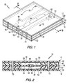
- Fig. 1 is a perspective view illustrating one embodiment, and
- Fig. 2 is a sectional view taken along line 2-2 looking in the direction of the arrows in Fig. 1.
-
- The air-
dielectric stripline 10 illustrated in Figs. 1 and 2 includes a laminated structure including a plurality of planar dielectric layers constructed of suitable non-conductive material of the type used for printed circuit boards. This structure includes a topdielectric layer 12, an intermediatedielectric layer 14 and a bottomdielectric layer 16. These layers are spaced from each other in parallel planes withlayer 14 being locatedintermediate layers layer 12 has anupper face 18 and alower face 20.Layer 14 has anupper face 22 and alower face 24.Layer 16 has anupper face 26 and alower face 28. -
Ground planes layers Ground plane 30 is attached to thelower face 20 of thetop layer 18 whereasground plane 32 is attached to theupper face 26 ofbottom layer 16.Ground plane 30 is spaced from theupper face 22 oflayer 14 by means of a planardielectric spacer layer 40. Similarly,ground plane 32 is spaced from thelower face 24 oflayer 14 by means of a planardielectric spacer layer 42.Layers layers layers - A channel is formed in each of the
spacer layers channel 50 of rectangular cross-section, as viewed in Fig. 2, is formed inspacer layer 40 and extends longitudinally (into the paper). This channel together withlayers channel 52 is formed inspacer layer 42. - An upper conductive
inner trace 60 is attached to theupper face 22 of theintermediate layer 14. A lower conductiveinner trace 62 in registry withtrace 60 is attached to thelower surface 24 oflayer 14. Thetraces channels vias 64 which extend between the traces through theintermediate layer 14. Thevias 64, as is well known in the art, take the form of conductive plated through holes inlayer 14. Thesevias 64 place theconductive traces -
Ground planes vias vias - The voltage gradients of the stripline are primarily across the air-dielectric in
channels - Air cooling of the stripline may be obtained by air flowing through
channels suitable inlet passage 80 inlayer 12 so that air may flow into thechamber 50 and thence longitudinally along theupper trace 60 and exit as through anexit passageway 82. A similar inlet passageway and exit passageway are provided inlayer 16 for connection withchannel 52. - The air-dielectric stripline, may be manufactured using conventional printed wiring board (PWB) fabrication techniques. This preserves much of the low-cost characteristics of PWBs while attaining a low-dielectric constant which is close to 1.0 and subsequent low conductor losses of the air-dielectric stripline. The construction also allows for high power transmission, by a forced-air cooling of the stripline by air flowing through
channels - The construction is in the following manner. The intermediate
dielectric layer 14 may be initially metalized on both itsupper face 22 and itslower face 24. Theconductive traces layer 14. The plurality of longitudinally spaced vias may be formed to electrically connecttraces bottom layer 16 may be provided with itsupper face 26 metalized to provide theground plane 32. Also, theupper layer 12 may have itslower surface 20 metalized to provide theground plane 30. Spacer layers 40 and 42 may then havechannels vias 70 may then be formed so as to electrically interconnect ground planes 30 and 32. Also, longitudinally spacedvias 72 are formed for interconnecting ground planes 30 and 32. Thereafter, the assembly may be suitably heated so that bonding agents and the like will cause the assembly to be bonded together. - In an alternative arrangement, layers 12 and 40 may be integral as a single layer with
channel 50 formed therein. The roof of the channel would have attached thereto a ground plane, such asplane 30. Also, layers 16 and 42 may be integral as a single layer with achannel 52 formed therein. The floor of this channel would have attached thereto a ground plane, such asplane 32. The ground planes would be interconnected as by vias.
Claims (3)
- An air-dielectric stripline (10) multiple solid layer laminated structure comprising top, (12) intermediate, (14) and bottom planar dielectric layers (16) spaced from each other in parallel planes with said intermediate layer being located intermediate said top and bottom layers and each layer having upper and lower oppositely directed faces, first and second electrically conductive planar ground planes (30, 32) respectively attached to the lower surface (20) of said top layer and upper surface (22) of said bottom layer; first and second planar dielectric spacer layers (40 and 42) respectively located between said top and intermediate layers and said intermediate and bottom layers for maintaining said spacing between top, intermediate and bottom layers, each said spacer layer having a channel (50 52) formed therein with longitudinally extending solid sidewalls in said spacer defining upper and lower air chambers on opposing faces of said intermediate layer, said channels being adapted for cooling by air flowing forced through said chambers during operation, characterized in that a first (60) and a second (62) conductive inner traces are attached respectively to the upper (22) and lower (24) faces of said intermediate layer within said chambers and spaced from an associated ground plane (30,32) by the thickness of said spacer dielectric layer, with said first and second traces arranged in parallel to each other including means (64) for electrically interconnecting said first and second traces so as to be substantially at the same electrical potential and further comprising, for each chamber defined by said intermediate layer (14) and respectively said top (12) and bottom (16) layer, an inlet passage (80) whereby air may flow into said chamber and thence longitudinally along said trace (60, 62) and exit through an exit passageway (82), said inlet passage (80) and said outlet passageway (82) being formed on the top layer (12) and the bottom layer (16) for respectively the upper (50) and lower (52) air chambers.
- A stripline as claimed in claim 1 characterized in that said means (64) for interconnecting includes a plurality of conductive vias extending from said first trace to said second trace through said intermediate layer.
- A stripline as claimed in claim 1 or 2 including means (70 and 72) for electrically interconnecting first and second ground planes so as to be substantially at the same electrical potential, in which said means for connecting said first and second ground planes include a plurality of electrically conductive vias (70 and 72) extending between said ground planes through said spacer dielectric layers and said intermediate dielectric layer.
Applications Claiming Priority (2)
| Application Number | Priority Date | Filing Date | Title |
|---|---|---|---|
| US631580 | 1996-04-12 | ||
| US08/631,580 US5712607A (en) | 1996-04-12 | 1996-04-12 | Air-dielectric stripline |
Publications (2)
| Publication Number | Publication Date |
|---|---|
| EP0801433A1 EP0801433A1 (en) | 1997-10-15 |
| EP0801433B1 true EP0801433B1 (en) | 2002-09-25 |
Family
ID=24531831
Family Applications (1)
| Application Number | Title | Priority Date | Filing Date |
|---|---|---|---|
| EP97400544A Expired - Lifetime EP0801433B1 (en) | 1996-04-12 | 1997-03-12 | Air-dielectric stripline |
Country Status (5)
| Country | Link |
|---|---|
| US (1) | US5712607A (en) |
| EP (1) | EP0801433B1 (en) |
| JP (1) | JPH1041710A (en) |
| CA (1) | CA2199655C (en) |
| DE (1) | DE69715715T2 (en) |
Families Citing this family (74)
| Publication number | Priority date | Publication date | Assignee | Title |
|---|---|---|---|---|
| SE512166C2 (en) * | 1997-11-21 | 2000-02-07 | Ericsson Telefon Ab L M | Microstrip arrangement |
| US7106151B1 (en) * | 1998-07-24 | 2006-09-12 | Lucent Technologies Inc. | RF/microwave stripline structures and method for fabricating same |
| US6163233A (en) * | 1998-07-30 | 2000-12-19 | Harris Corporation | Waveguide with signal track cross-over and variable features |
| JP3255118B2 (en) * | 1998-08-04 | 2002-02-12 | 株式会社村田製作所 | Transmission line and transmission line resonator |
| US6414573B1 (en) * | 2000-02-16 | 2002-07-02 | Hughes Electronics Corp. | Stripline signal distribution system for extremely high frequency signals |
| DE10006964C2 (en) * | 2000-02-16 | 2002-01-31 | Infineon Technologies Ag | Electronic component with a conductive connection between two conductive layers and method for producing an electronic component |
| US6507320B2 (en) | 2000-04-12 | 2003-01-14 | Raytheon Company | Cross slot antenna |
| US6535088B1 (en) * | 2000-04-13 | 2003-03-18 | Raytheon Company | Suspended transmission line and method |
| US6622370B1 (en) | 2000-04-13 | 2003-09-23 | Raytheon Company | Method for fabricating suspended transmission line |
| US6518844B1 (en) * | 2000-04-13 | 2003-02-11 | Raytheon Company | Suspended transmission line with embedded amplifier |
| US6542048B1 (en) * | 2000-04-13 | 2003-04-01 | Raytheon Company | Suspended transmission line with embedded signal channeling device |
| US6552635B1 (en) * | 2000-04-13 | 2003-04-22 | Raytheon Company | Integrated broadside conductor for suspended transmission line and method |
| AU2001253249A1 (en) * | 2000-04-13 | 2001-10-30 | Raytheon Company | Suspended transmission line and method |
| DE10023736A1 (en) | 2000-05-15 | 2001-11-22 | Harting Elektrooptische Bauteile Gmbh & Co Kg | Printed circuit board and method for producing a printed circuit board |
| US6600395B1 (en) | 2000-12-28 | 2003-07-29 | Nortel Networks Limited | Embedded shielded stripline (ESS) structure using air channels within the ESS structure |
| US6603376B1 (en) | 2000-12-28 | 2003-08-05 | Nortel Networks Limited | Suspended stripline structures to reduce skin effect and dielectric loss to provide low loss transmission of signals with high data rates or high frequencies |
| US6621384B1 (en) | 2000-12-28 | 2003-09-16 | Nortel Networks Limited | Technology implementation of suspended stripline within multi-layer substrate used to vary time delay and to maximize the reach of signals with high data rates or high frequencies |
| US20040048420A1 (en) * | 2002-06-25 | 2004-03-11 | Miller Ronald Brooks | Method for embedding an air dielectric transmission line in a printed wiring board(PCB) |
| DE602004028349D1 (en) | 2003-03-04 | 2010-09-09 | Rohm & Haas Elect Mat | COAXIAL WAVEEL MEMORY STRUCTURES AND PROCEDURES FOR THEIR EDUCATION |
| US6885264B1 (en) | 2003-03-06 | 2005-04-26 | Raytheon Company | Meandered-line bandpass filter |
| US7145414B2 (en) * | 2003-06-30 | 2006-12-05 | Endwave Corporation | Transmission line orientation transition |
| WO2006007803A1 (en) * | 2004-07-20 | 2006-01-26 | Technische Universität Braunschweig Carolo-Wilhelmina | Cooled integrated circuit |
| KR100654703B1 (en) | 2004-08-09 | 2006-12-06 | 주식회사 극동통신 | Support Structure of Honeycomb Air Stripline |
| US7400214B2 (en) * | 2004-08-30 | 2008-07-15 | Powerwave Technologies, Inc. | Low loss, high power air dielectric stripline edge coupling structure |
| US7663064B2 (en) * | 2004-09-25 | 2010-02-16 | Banpil Photonics, Inc. | High-speed flex printed circuit and method of manufacturing |
| NL1027641C2 (en) * | 2004-12-02 | 2006-06-07 | Thales Nederland Bv | Radio microwave structure involves phased array antennas based on relative technology |
| US7276989B2 (en) * | 2005-06-02 | 2007-10-02 | Raytheon Company | Attenuator circuit comprising a plurality of quarter wave transformers and lump element resistors |
| EP1939137B1 (en) * | 2006-12-30 | 2016-08-24 | Nuvotronics, LLC | Three-dimensional microstructures and methods of formation thereof |
| KR101472134B1 (en) | 2007-03-20 | 2014-12-15 | 누보트로닉스, 엘.엘.씨 | Coaxial transmission line microstructure and method of forming the same |
| US7755174B2 (en) | 2007-03-20 | 2010-07-13 | Nuvotonics, LLC | Integrated electronic components and methods of formation thereof |
| EP2160791A1 (en) * | 2007-06-28 | 2010-03-10 | BAE Systems PLC | Microwave circuit assembly |
| KR100987191B1 (en) * | 2008-04-18 | 2010-10-11 | (주)기가레인 | Printed circuit board with the bonding sheet around the signal transmission line removed |
| US8659371B2 (en) * | 2009-03-03 | 2014-02-25 | Bae Systems Information And Electronic Systems Integration Inc. | Three-dimensional matrix structure for defining a coaxial transmission line channel |
| US7978029B2 (en) * | 2009-05-09 | 2011-07-12 | Research Triangle Institute | Multiple-layer signal conductor |
| US8049578B1 (en) * | 2009-08-17 | 2011-11-01 | Ball Aerospace & Technologies Corp. | Air loaded stripline |
| US8164397B2 (en) * | 2009-08-17 | 2012-04-24 | International Business Machines Corporation | Method, structure, and design structure for an impedance-optimized microstrip transmission line for multi-band and ultra-wide band applications |
| US8264848B2 (en) | 2009-10-30 | 2012-09-11 | Research In Motion Limited | Electrical assembly having impedance controlled signal traces |
| US20110123783A1 (en) | 2009-11-23 | 2011-05-26 | David Sherrer | Multilayer build processses and devices thereof |
| US8917150B2 (en) | 2010-01-22 | 2014-12-23 | Nuvotronics, Llc | Waveguide balun having waveguide structures disposed over a ground plane and having probes located in channels |
| JP5639194B2 (en) | 2010-01-22 | 2014-12-10 | ヌボトロニクス,エルエルシー | Thermal control |
| CN102378501B (en) * | 2010-07-13 | 2013-06-26 | 富葵精密组件(深圳)有限公司 | Circuit board manufacturing method |
| JP5666270B2 (en) | 2010-11-29 | 2015-02-12 | 株式会社ヨコオ | Signal transmission medium, high-frequency signal transmission medium |
| US8866300B1 (en) | 2011-06-05 | 2014-10-21 | Nuvotronics, Llc | Devices and methods for solder flow control in three-dimensional microstructures |
| US8814601B1 (en) | 2011-06-06 | 2014-08-26 | Nuvotronics, Llc | Batch fabricated microconnectors |
| JP6335782B2 (en) | 2011-07-13 | 2018-05-30 | ヌボトロニクス、インク. | Method for fabricating electronic and mechanical structures |
| US9325044B2 (en) | 2013-01-26 | 2016-04-26 | Nuvotronics, Inc. | Multi-layer digital elliptic filter and method |
| US9306254B1 (en) | 2013-03-15 | 2016-04-05 | Nuvotronics, Inc. | Substrate-free mechanical interconnection of electronic sub-systems using a spring configuration |
| US9306255B1 (en) | 2013-03-15 | 2016-04-05 | Nuvotronics, Inc. | Microstructure including microstructural waveguide elements and/or IC chips that are mechanically interconnected to each other |
| JP6285638B2 (en) | 2013-04-25 | 2018-02-28 | 日本メクトロン株式会社 | Printed wiring board and printed wiring board manufacturing method |
| EP3095159A4 (en) | 2014-01-17 | 2017-09-27 | Nuvotronics, Inc. | Wafer scale test interface unit: low loss and high isolation devices and methods for high speed and high density mixed signal interconnects and contactors |
| US10847469B2 (en) | 2016-04-26 | 2020-11-24 | Cubic Corporation | CTE compensation for wafer-level and chip-scale packages and assemblies |
| EP3224899A4 (en) | 2014-12-03 | 2018-08-22 | Nuvotronics, Inc. | Systems and methods for manufacturing stacked circuits and transmission lines |
| CN105792501B (en) * | 2014-12-23 | 2018-10-30 | 鹏鼎控股(深圳)股份有限公司 | Circuit board and preparation method thereof |
| WO2017130731A1 (en) * | 2016-01-27 | 2017-08-03 | 株式会社村田製作所 | Signal transmission line |
| US10347961B2 (en) * | 2016-10-26 | 2019-07-09 | Raytheon Company | Radio frequency interconnect systems and methods |
| US9883578B1 (en) | 2016-12-21 | 2018-01-30 | Deere & Company | Cooling conductive trace with pressurized air or gas |
| US10319654B1 (en) | 2017-12-01 | 2019-06-11 | Cubic Corporation | Integrated chip scale packages |
| KR101938105B1 (en) | 2018-01-25 | 2019-01-14 | 주식회사 기가레인 | Flexible circuit board with improved bonding position accuracy |
| US10257921B1 (en) | 2018-04-12 | 2019-04-09 | Google Llc | Embedded air gap transmission lines |
| CN108511858B (en) * | 2018-04-13 | 2020-04-14 | 京东方科技集团股份有限公司 | A liquid crystal phase shifter and electronic equipment |
| CN108633167A (en) * | 2018-05-28 | 2018-10-09 | 维沃移动通信有限公司 | A circuit board, signal transmission line and manufacturing method thereof |
| US11043727B2 (en) | 2019-01-15 | 2021-06-22 | Raytheon Company | Substrate integrated waveguide monopulse and antenna system |
| CN111755806A (en) | 2019-03-29 | 2020-10-09 | 康普技术有限责任公司 | Radiators and Base Station Antennas for Antennas |
| EP3859881A1 (en) * | 2020-01-29 | 2021-08-04 | Nokia Shanghai Bell Co., Ltd. | Antenna component |
| KR102896737B1 (en) * | 2020-03-18 | 2025-12-08 | 삼성전자주식회사 | Printed circuit board including ground trace |
| CN113747654B (en) * | 2020-05-27 | 2023-08-04 | 宏启胜精密电子(秦皇岛)有限公司 | Flexible circuit board and manufacturing method thereof |
| CN112105150B (en) * | 2020-11-04 | 2021-08-13 | 生益电子股份有限公司 | A method for making a buried cavity and a PCB |
| CN112261802B (en) * | 2020-11-04 | 2021-08-13 | 生益电子股份有限公司 | A method for making a buried cavity and a PCB |
| JP7355256B2 (en) | 2020-11-30 | 2023-10-03 | 株式会社村田製作所 | Transmission lines and electronic equipment |
| WO2022113618A1 (en) * | 2020-11-30 | 2022-06-02 | 株式会社村田製作所 | Transmission line and electronic device |
| JP7327690B2 (en) * | 2020-11-30 | 2023-08-16 | 株式会社村田製作所 | Transmission lines and electronic equipment |
| JP7559833B2 (en) * | 2020-11-30 | 2024-10-02 | 株式会社村田製作所 | Transmission lines and electronic devices |
| IT202100011000A1 (en) * | 2021-04-30 | 2022-10-30 | Commscope Italy Srl | STRIPLINE BIAS TEE MADE WITH CAPACITY TO THE GROUND |
| JPWO2023176643A1 (en) * | 2022-03-17 | 2023-09-21 |
Citations (1)
| Publication number | Priority date | Publication date | Assignee | Title |
|---|---|---|---|---|
| WO1995021472A1 (en) * | 1994-02-03 | 1995-08-10 | Hollandse Signaalapparaten B.V. | Transmission-line network |
Family Cites Families (6)
| Publication number | Priority date | Publication date | Assignee | Title |
|---|---|---|---|---|
| US2913686A (en) * | 1953-09-17 | 1959-11-17 | Cutler Hammer Inc | Strip transmission lines |
| US2812501A (en) * | 1954-03-04 | 1957-11-05 | Sanders Associates Inc | Transmission line |
| US2964718A (en) * | 1955-03-21 | 1960-12-13 | Cutler Hammer Inc | Microwave circuits |
| US3518688A (en) * | 1965-11-22 | 1970-06-30 | Itt | Microwave strip transmission line adapted for integral slot antenna |
| FR2496996A1 (en) * | 1980-12-18 | 1982-06-25 | Thomson Csf | HYPERFREQUENCY TRANSMISSION LINE OF THE AIR TRIPLAQUE TYPE AND USES THEREOF |
| US4614922A (en) * | 1984-10-05 | 1986-09-30 | Sanders Associates, Inc. | Compact delay line |
-
1996
- 1996-04-12 US US08/631,580 patent/US5712607A/en not_active Expired - Lifetime
-
1997
- 1997-03-11 CA CA002199655A patent/CA2199655C/en not_active Expired - Fee Related
- 1997-03-12 DE DE69715715T patent/DE69715715T2/en not_active Expired - Fee Related
- 1997-03-12 EP EP97400544A patent/EP0801433B1/en not_active Expired - Lifetime
- 1997-04-10 JP JP9092267A patent/JPH1041710A/en not_active Withdrawn
Patent Citations (1)
| Publication number | Priority date | Publication date | Assignee | Title |
|---|---|---|---|---|
| WO1995021472A1 (en) * | 1994-02-03 | 1995-08-10 | Hollandse Signaalapparaten B.V. | Transmission-line network |
Also Published As
| Publication number | Publication date |
|---|---|
| DE69715715D1 (en) | 2002-10-31 |
| US5712607A (en) | 1998-01-27 |
| DE69715715T2 (en) | 2003-08-14 |
| EP0801433A1 (en) | 1997-10-15 |
| CA2199655C (en) | 2005-01-25 |
| CA2199655A1 (en) | 1997-10-12 |
| JPH1041710A (en) | 1998-02-13 |
Similar Documents
| Publication | Publication Date | Title |
|---|---|---|
| US5712607A (en) | Air-dielectric stripline | |
| US4494083A (en) | Impedance matching stripline transition for microwave signals | |
| EP0439928B1 (en) | Directional stripline structure and manufacture | |
| US4614922A (en) | Compact delay line | |
| US5408053A (en) | Layered planar transmission lines | |
| US5561405A (en) | Vertical grounded coplanar waveguide H-bend interconnection apparatus | |
| US5315072A (en) | Printed wiring board having blind holes | |
| US5569488A (en) | Method of making multi-dielectric laminates | |
| JPH10303608A (en) | Dielectric waveguide line and multilayer wiring board including the same | |
| JPH04233794A (en) | Multilayer circuit board assembly and its manufacture | |
| US20090107710A1 (en) | Differential trace profile for printed circult boards | |
| CN101095381A (en) | Printed circuit boards for high-speed electrical connectors | |
| US4772864A (en) | Multilayer circuit prototyping board | |
| EP1032957A2 (en) | Microstrip arrangement | |
| WO1994002970A1 (en) | Rf waveguide signal transition apparatus | |
| CA1300708C (en) | Solderless, pushdown connectors for rf and dc | |
| US6800939B2 (en) | Apparatus and method for providing low-loss transmission lines in interconnected mesh plane systems | |
| JP3347607B2 (en) | Laminated waveguide line | |
| CA2586290A1 (en) | Single or multi-layer printed circuit board with improved via design | |
| US6727435B1 (en) | Backplane power distribution system | |
| EP0543979B1 (en) | A device comprising laminated conductive patterns and easily selectable dielectrics | |
| US5384555A (en) | Combined RF and digital/DC signalling interconnect laminate | |
| JPH0680964B2 (en) | Circuit device having stripline | |
| JPH07109942B2 (en) | Flexible rigid printed wiring board | |
| KR100256627B1 (en) | Backward wave hybrid coupler for surface mounting device |
Legal Events
| Date | Code | Title | Description |
|---|---|---|---|
| PUAI | Public reference made under article 153(3) epc to a published international application that has entered the european phase |
Free format text: ORIGINAL CODE: 0009012 |
|
| AK | Designated contracting states |
Kind code of ref document: A1 Designated state(s): CH DE FR GB IT LI |
|
| 17P | Request for examination filed |
Effective date: 19970919 |
|
| 17Q | First examination report despatched |
Effective date: 19990125 |
|
| GRAG | Despatch of communication of intention to grant |
Free format text: ORIGINAL CODE: EPIDOS AGRA |
|
| GRAG | Despatch of communication of intention to grant |
Free format text: ORIGINAL CODE: EPIDOS AGRA |
|
| GRAH | Despatch of communication of intention to grant a patent |
Free format text: ORIGINAL CODE: EPIDOS IGRA |
|
| GRAH | Despatch of communication of intention to grant a patent |
Free format text: ORIGINAL CODE: EPIDOS IGRA |
|
| GRAA | (expected) grant |
Free format text: ORIGINAL CODE: 0009210 |
|
| AK | Designated contracting states |
Kind code of ref document: B1 Designated state(s): CH DE FR GB IT LI |
|
| PG25 | Lapsed in a contracting state [announced via postgrant information from national office to epo] |
Ref country code: LI Free format text: LAPSE BECAUSE OF FAILURE TO SUBMIT A TRANSLATION OF THE DESCRIPTION OR TO PAY THE FEE WITHIN THE PRESCRIBED TIME-LIMIT Effective date: 20020925 Ref country code: CH Free format text: LAPSE BECAUSE OF FAILURE TO SUBMIT A TRANSLATION OF THE DESCRIPTION OR TO PAY THE FEE WITHIN THE PRESCRIBED TIME-LIMIT Effective date: 20020925 |
|
| REG | Reference to a national code |
Ref country code: GB Ref legal event code: FG4D |
|
| REG | Reference to a national code |
Ref country code: CH Ref legal event code: EP |
|
| REF | Corresponds to: |
Ref document number: 69715715 Country of ref document: DE Date of ref document: 20021031 |
|
| ET | Fr: translation filed | ||
| PG25 | Lapsed in a contracting state [announced via postgrant information from national office to epo] |
Ref country code: GB Free format text: LAPSE BECAUSE OF NON-PAYMENT OF DUE FEES Effective date: 20030312 |
|
| REG | Reference to a national code |
Ref country code: CH Ref legal event code: PL |
|
| PLBE | No opposition filed within time limit |
Free format text: ORIGINAL CODE: 0009261 |
|
| STAA | Information on the status of an ep patent application or granted ep patent |
Free format text: STATUS: NO OPPOSITION FILED WITHIN TIME LIMIT |
|
| 26N | No opposition filed |
Effective date: 20030626 |
|
| GBPC | Gb: european patent ceased through non-payment of renewal fee |
Effective date: 20030312 |
|
| PG25 | Lapsed in a contracting state [announced via postgrant information from national office to epo] |
Ref country code: IT Free format text: LAPSE BECAUSE OF NON-PAYMENT OF DUE FEES;WARNING: LAPSES OF ITALIAN PATENTS WITH EFFECTIVE DATE BEFORE 2007 MAY HAVE OCCURRED AT ANY TIME BEFORE 2007. THE CORRECT EFFECTIVE DATE MAY BE DIFFERENT FROM THE ONE RECORDED. Effective date: 20050312 |
|
| PGFP | Annual fee paid to national office [announced via postgrant information from national office to epo] |
Ref country code: FR Payment date: 20070319 Year of fee payment: 11 |
|
| PGFP | Annual fee paid to national office [announced via postgrant information from national office to epo] |
Ref country code: DE Payment date: 20080630 Year of fee payment: 12 |
|
| REG | Reference to a national code |
Ref country code: FR Ref legal event code: ST Effective date: 20081125 |
|
| PG25 | Lapsed in a contracting state [announced via postgrant information from national office to epo] |
Ref country code: FR Free format text: LAPSE BECAUSE OF NON-PAYMENT OF DUE FEES Effective date: 20080331 |
|
| PG25 | Lapsed in a contracting state [announced via postgrant information from national office to epo] |
Ref country code: DE Free format text: LAPSE BECAUSE OF NON-PAYMENT OF DUE FEES Effective date: 20091001 |