EP0798950A2 - High voltage noise filter and magnetron device using it - Google Patents
High voltage noise filter and magnetron device using it Download PDFInfo
- Publication number
- EP0798950A2 EP0798950A2 EP97104923A EP97104923A EP0798950A2 EP 0798950 A2 EP0798950 A2 EP 0798950A2 EP 97104923 A EP97104923 A EP 97104923A EP 97104923 A EP97104923 A EP 97104923A EP 0798950 A2 EP0798950 A2 EP 0798950A2
- Authority
- EP
- European Patent Office
- Prior art keywords
- conductive
- layer
- noise filter
- high voltage
- voltage noise
- Prior art date
- Legal status (The legal status is an assumption and is not a legal conclusion. Google has not performed a legal analysis and makes no representation as to the accuracy of the status listed.)
- Granted
Links
Images


Classifications
-
- H—ELECTRICITY
- H01—ELECTRIC ELEMENTS
- H01J—ELECTRIC DISCHARGE TUBES OR DISCHARGE LAMPS
- H01J23/00—Details of transit-time tubes of the types covered by group H01J25/00
- H01J23/14—Leading-in arrangements; Seals therefor
- H01J23/15—Means for preventing wave energy leakage structurally associated with tube leading-in arrangements, e.g. filters, chokes, attenuating devices
-
- H—ELECTRICITY
- H01—ELECTRIC ELEMENTS
- H01F—MAGNETS; INDUCTANCES; TRANSFORMERS; SELECTION OF MATERIALS FOR THEIR MAGNETIC PROPERTIES
- H01F27/00—Details of transformers or inductances, in general
- H01F27/28—Coils; Windings; Conductive connections
- H01F27/32—Insulating of coils, windings, or parts thereof
- H01F27/323—Insulation between winding turns, between winding layers
-
- H—ELECTRICITY
- H01—ELECTRIC ELEMENTS
- H01F—MAGNETS; INDUCTANCES; TRANSFORMERS; SELECTION OF MATERIALS FOR THEIR MAGNETIC PROPERTIES
- H01F37/00—Fixed inductances not covered by group H01F17/00
-
- H—ELECTRICITY
- H01—ELECTRIC ELEMENTS
- H01F—MAGNETS; INDUCTANCES; TRANSFORMERS; SELECTION OF MATERIALS FOR THEIR MAGNETIC PROPERTIES
- H01F27/00—Details of transformers or inductances, in general
- H01F27/28—Coils; Windings; Conductive connections
- H01F27/32—Insulating of coils, windings, or parts thereof
- H01F2027/329—Insulation with semiconducting layer, e.g. to reduce corona effect
Definitions
- the present invention relates to a high voltage noise filter for use in microwave devices and a magnetron device incorporating such a high voltage noise filter.
- FIG. 10 is a bottom end view illustrating a relevant portion of a magnetron incorporating a conventional high voltage noise filter 1.
- stem terminals 5a and 5b are connected with conductive wires 2a and 2b partially wound into coils, respectively, for prevention of leakage of fundamental wave noise and higher harmonic noise from the respective stem terminals 5a and 5b of the magnetron.
- the conductive wires 2a and 2b are coated with an insulating material along the overall length thereof except for end portions 30a and 30b connected with the respective stem terminals 5a and 5b.
- At coil portions defining choke coils 4a and 4b, and the conductive wires 2a and 2b are coated with insulating layers 1a and 1b.
- conductive layers 34a and 34b are formed on the aforesaid insulating layers 1a and 1b.
- the conductive wires 2a and 2b have only the insulating layers 1a and 1b at end portions 31a and 31b of the coil portions 3a and 3b, and terminals thereof are connected to respective fastening tabs (terminals) 7a and 7b to be connected to a microwave source 6.
- the coil portions 3a and 3b are accommodated in cylindrical conductive members 8a and 8b, respectively.
- FIG. 10 shows a cross-section of the cylindrical conductive members 8a and 8b for illustration of the coil portions 3a and 3b.
- the cylindrical conductive members 8a and 8b are accommodated in resin casings 16a and 16b.
- the conductive members 8a and 8b accommodating the coil portions 3a and 3b, the terminal portions 31a and 31b and joints between the fastening tabs 7a and 7b and the terminal portions 31a and 31b are filled with an insulating resin material 11.
- the conductive members 8a and 8b are electrically connected with a filter casing 10 by way of grounding plates 9.
- terminal regions 1e and 1f of the coil portions 3a and 3b may sometimes suffer an abnormal increase in the electric field strength in the vicinity of the end portions of the conductive layers 34a and 34b, which increase in the electric field strength tends to cause insulation breakdown near the end portions of the conductive layers.
- the prevention of the insulation breakdown requires an increase in the withstand voltage characteristics of the insulating layers 1a and 1b of the conductive materials 2a and 2b.
- an increase in the withstand voltage characteristics requires the insulating layers 1a and 1b to have an extreme thickness.
- An increased thickness of the insulating layers 1a and 1b leads to an increased size of the coil portions 3a and 3b. This results in not only a larger size of the high voltage noise filter but also decrease in the capacitance between the outer peripheral surfaces of the coil portions 3a and 3b and the conductive wires 2a and 2b. Consequently, the noise filter suffers a serious deterioration of the characteristics thereof.
- the present invention is directed to relaxation of concentration of the aforesaid electric field in the vicinity of the end portions of the conductive layers without increasing the thickness of the insulating layers 1a and 1b thereby improving the withstand voltage characteristics of the high voltage noise filter.
- the present invention has been made through experimental study and development after many experiments on examples.
- a high voltage noise filter in accordance with the invention comprises a coil-shaped conductive wire for producing an inductive component, an insulating layer for producing a capacitance component formed on the surface of the conductive wire, and a conductive layer formed on at least a part of the insulating layer by means of spraying or depositing a metal material.
- the capacitance component is produced by the conductive wire, insulating layer and conductive layer.
- the high voltage noise filter further comprises a high withstand voltage layer comprising either a semiconductive layer or an insulative member layer, and the high withstand voltage layer is formed at least in the vicinity of an end portion of the conductive layer as interposed between the outer peripheral surface of the insulating layer and the conductive layer.
- the insulating layer is improved in the withstand voltage characteristics thereof for enhancing the reliability.
- the insulating layer can be reduced in thickness, thus providing a high voltage noise filter of small size at low costs.
- the coil-shaped conductive wire comprising the conductive layer is accommodated in a cylindrical conductive member.
- the conductive layer formed on the outer periphery of the insulating layer is in contact with the interior wall of the cylindrical conductive member, defining multiple contacting portions therewith.
- the conductive layer and a grounding plate are connected with each other at a low resistance thorough the cylindrical conductive member electrically connected to the grounding plate, a potential of the conductive layer lowers and the electric field concentration in the vicinity of the end portion of the conductive layer is further relaxed. Therefore the insulating layer of the coil-shaped conductive wire is notably improved in the withstand voltage characteristics, resulting in an enhanced reliability.
- the aforesaid semiconductive layer comprises a material ranging from 10 -4 to 10 6 ⁇ m in electric resistivity.
- the electric field strength in the vicinity of the end portion of the conductive layer is reduced by employing the semiconductive layer ranging from 10 -4 to 10 6 ⁇ m in electric resistivity as the high withstand voltage layer.
- the aforesaid insulative member comprises a polyimide resin material.
- the electric field strength in the vicinity of the end portion of the conductive layer is reduced by forming the high withstand voltage layer of the polyimide resin material.
- the aforesaid insulative member comprises a silicone resin material.
- the electric field strength in the vicinity of the end portion of the conductive layer is reduced by forming the high withstand voltage layer of the silicone resin material.
- a magnetron device in accordance with the invention incorporates a high voltage noise filter comprising a coil-shaped conductive wire for producing an inductive component, an insulating layer for producing a capacitance component formed on the surface of the conductive wire, a conductive layer partially formed on the insulating layer, and a high withstand voltage layer comprising either a semiconductive layer or an insulative member layer formed at least in the vicinity of an end portion of the conductive layer as interposed between the outer peripheral surface of the insulating layer and the conductive layer.
- the magnetron device of the invention is improved in reliability because of the incorporation of the high voltage noise filter improved in the withstand voltage characteristics, the noise filter characterized by the high withstand voltage layer formed in the vicinity of the end portion of the conductive layer of the coil-shaped conductive wire as interposed between the outer peripheral surface of the insulating layer and the conductive layer.
- a magnetron device incorporates a high voltage noise filter wherein the coil-shaped conducive wire having the insulating layer and conductive layer is accommodated in a cylindrical conductive member.
- the high voltage noise filter can achieve a significant improvement in the withstand voltage characteristics by way of accommodation of the coil-shaped conductive wire in the cylindrical conductive member and hence, the magnetron device incorporating such a high voltage noise filter is notably improved in the reliability.
- FIG. 1 is a top plan view illustrating a high voltage noise filter in accordance with a first embodiment of the invention.
- conductive wires 2a and 2b for producing an inductive component of an impedance are formed of a copper or aluminum wire having a diameter of from 1 to 2 mm.
- the conductive wires 2a and 2b are of a bare wire free of an insulative coating at portions shown by rough hatching for connection with unillustrated stem terminals of a magnetron.
- the conductive wires 2a and 2b were coated with a 30 to 500 ⁇ m thick, preferably about 300 ⁇ m thick, insulating layer formed of a heat-resistant resin material e.g. fluororesin.
- Choke coils 4a and 4b were formed of 15 to 25mm-long coated wires 29a and 29b wound into coils 10 to 20 mm in outer diameter.
- the choke coils 4a and 4b receive cores 4c and 4d, such as formed of ferrite, in hollow portions thereof, respectively.
- Coil portions 3a and 3b formed of the coated wires extending via terminal portions 4e and 4f of the choke coils 4a and 4b have a greater outer diameter than the choke coils 4a and 4b.
- the coated wires 29a and 29b have conductive layers 34a and 34b formed further on the coatings of a heat-resistant, which is similar to the above-mentioned resin, such as fluororesin.
- the conductive layers 34a and 34b were formed by spraying or depositing at least one type of metal materials including zinc, solder, copper, silver plate and the like.
- FIG. 1 illustrates the portions of the coated wires 29a and 29b on which the conductive layers 34a and 34b are formed. Capacitors were formed by the aforesaid conductive wires 2a and 2b, coatings 33a and 33b, and conductive layers 34a and 34b.
- FIG. 2A is a side elevation view of the coil portion 3b shown in FIG. 1.
- the coil portion 3a has the same shape and size as the coil portion 3b except for that the coil portion 3a was wound in the opposite direction (in a symmetrical form) to the coil portion 3b. Accordingly, description on FIG. 2A through FIG. 2C illustrating the coil portion 3b is similarly applicable to the coil portion 3a. Therefore, FIG. 2A through FIG. 2C give reference marks of the components of the coil portion 3a accompanied by corresponding reference marks of those of the coil portion 3b.
- FIG. 2B is a sectional view of terminal portions 1c and 1d of boundary regions 12a and 12b taken on the line b-b of FIG. 2A, the terminal portions being continuous to the coated wires 29a and 29b.
- the terminal portions 1c and 1d have double-layered structures, wherein the outer peripheries of the conductive wires 2a and 2b were coated with the coatings 33a and 33b of insulating layers.
- the insulating layers are preferably of fluororesin, but other material such as polyimide resin, silicon resin or the like can be used similarly.
- the outer peripheries of the coatings 33a and 33b are covered with high withstand voltage layers 35a and 35b, respectively.
- FIG. 2C is a sectional view of terminal regions 1e and 1f taken on the line c-c of FIG. 2A.
- the terminal regions 1e and 1f have triple-layered structures, wherein the outer peripheries of the predetermined part (i.e., part except the end part) of the coatings 33a and 33b around the conductive wires 2a and 2b are coated with the high withstand voltage layers 35a and 35b, and the predetermined part (i.e., except the end part) of the outer peripheries of the high withstand voltage layers were covered with conductive layers 34a and 34b, respectively.
- the high withstand voltage layers 35a and 35b were formed on the coatings 33a and 33b of the coated wires 29a and 29b, as shown in FIG. 2A, FIG. 2B and FIG. 2C,
- the high withstand voltage layers 35a and 35b comprised a semiconductive layer or an insulative layer formed of a resin material such as polyimide, silicone or the like.
- the semiconductive layer has a midrange electric resistivity between those of the insulating material and conductive material, and preferably, it is in a range from 10 -4 to 10 6 ⁇ m in electric resistivity.
- Examples of preferred materials for the semiconductive layer include pyrite, germanium, cuprous oxide, selenium and the like. Such a material is pulverized and mixed with an insulating material so as to be formed into a film or tube.
- the resultant film or tube is wound around or put on the outer peripheries of the coatings 33a and 33b of the coated wires 29a and 29b thereby forming the semiconductive layers as the high withstand voltage layers 35a and 35b.
- polyimide resin material is used for the insulative members as the high withstand voltage layers 35a and 35b
- silicone resin material it is practical to put a silicone tube on the coatings or apply a silicone paste to the coatings of the coated wires.
- the conductive layers 34a and 34b are formed on the high withstand voltage layers 35a and 35b by spraying the aforesaid relatively soft metal material, e.g. zinc. Other material as solder or the like also can be used similarly.
- the terminal regions have the structures wherein the coatings 33a and 33b of the coated wires 29a and 29b are covered with the high withstand voltage layers 35a and 35b, and they are further coated with the conductive layers 34a and 34b such as of zinc or solder.
- the high withstand voltage layers 35a and 35b are also formed on boundary regions 32a and 32b extending from the coil portions 3a and 3b to fastening tabs 71 and 7b, respectively.
- terminal regions 3c and 3d at the other ends of the coil portions 3a and 3b have the triple-layered structures of the coatings 33a and 33b, the high withstand voltage layers 35a and 35b and the conductive layers 34a and 34b, respectively.
- the conductive layers 34a and 34b at the respective terminal portions 3c and 3d of the coil portions 3a and 3b are connected to grounding plates 9 by means of conductive members 14 such as of solder.
- the coil portions 3a and 3b are housed in a resin casing 16a shown by sectional form in FIG. 1.
- the boundary regions 32a and 32b of the coil portions 3a and 3b are housed in a resin casing 16b also shown by sectional form in FIG. 1.
- Terminals 12e and 12f of the coil portions 3a and 3b are connected to the respective fastening tabs 7a and 7b extending through the resin casing 16b to project outward of the casing 16b.
- the interior of the resin casings 16a and 16b is filled with an insulating resin material 11, such as an epoxy resin. Consequently, portions from the terminal portions 1c and 1d to the joints between the terminals 12e and 12f and the fastening tabs 7a and 7b are enclosed by the insulating resin 11.
- an insulating resin material 11 such as an epoxy resin.
- the terminal regions 1e and 1f as well as 3c and 3d of the coil portions 3a and 3b are made to the aforesaid triple-layered structure because the terminal regions 1e, 1f, 3c and 3d are places most likely to produce the electric field concentration and hence, are most susceptible to the insulation breakdown.
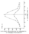
- FIG. 4 shows the results of a comparison between a wire material 40 of FIG. 3A according to the invention and a conventional wire material 41 of FIG. 3B having the double-layered structure.
- the wire materials extended in straight lines.
- the wire material 40 is used for the invention wherein the coil portions 3a and 3b have the triple-layered structures at the terminal regions 1e.
- a 0.3 mm thick fluororesin coating 33a is formed on the outer periphery of a copper conductive material 2a having a diameter of 1.4 mm.
- a 0.2 mm thick polyimide film 42 is formed as the high withstand voltage layer 35a within a range of 20 mm along the length of the wire with a central line P extending through the middle of the 20 mm range.
- a 0.1 mm thick solder layer is formed as the conductive layer 34a in a region extending rightward of the central line P.
- the conventional wire material 41 shown in FIG. 3B comprises the conductive layer 34a formed in the region rightward of the central line P, but does not include the polyimide film 42 as the high withstand voltage layer.
- the other parts of the wire material 41 are fabricated in the same manner as those of the wire material 40 shown in FIG. 3A.
- FIG. 4 graphically represents the calculation results.
- the numerals on the abscissa indicate the lateral distances along the wire materials 40 and 41 from the central line P indicative of the zero (middle) point.
- the numerals on the ordinate indicate the calculation values of the field strength.
- the wire material 40 of the invention notably reduces the electric field concentration.
- FIG. 1 The following test was conducted on the high voltage noise filter according to the embodiment hereof shown in FIG. 1.
- the conductive wires 2a and 2b, coatings 33a and 33b, high withstand voltage layers 35a and 35b, and conductive layers 34a and 34b of FIG. 2C were constructed in the same manner as those shown in FIG. 3A.
- a high voltage generating device 15 was connected across the fastening tabs 7a and 7b and the grounding plates 9 for applying AC voltage of from 5 kV to 18 kV.
- the test was conducted on the basis of ten samples, each ten samples including, as the high withstand voltage layers 35a and 35b, a semiconductive layer, polyimide film or silicone tube.
- FIG. 1 The test was conducted on the basis of ten samples, each ten samples including, as the high withstand voltage layers 35a and 35b, a semiconductive layer, polyimide film or silicone tube.
- FIG. 5 graphically represents measurements of voltage at which the coatings 33a and 33b produced insulation breakdown.
- dots indicate the insulation breakdown voltages (kV) of individual samples.
- a short lateral line intersecting the vertical line interconnecting the dots indicate the mean value of insulation breakdown voltages of each sample group.
- All the ten samples of the conventional noise filters without the high withstand voltage layers 35a and 35b, shown in FIG. 5, produced the insulation breakdown at voltages of from 7 to 10 kV, the mean value of which voltages was about 9 kV.
- the mean value of the insulation breakdown voltages was about 14 kV.
- the samples including the polyimide film and the silicone tube presented the mean insulation breakdown voltages of 16 kV and 14 kV, respectively. It is to be understood from the above results that the high voltage noise filters according to the embodiment hereof have achieved more than 50 % increase in the insulation breakdown voltage from that of the conventional high voltage noise filter.
- the high voltage noise filter employing the polyimide film in particular, has achieved a significant improvement in the withstand voltage characteristics, achieving more than 70 % increase in the insulation breakdown voltage.
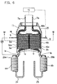
- FIG. 6 is a top plan view of a high voltage noise filter according to a second embodiment hereof.
- the choke coils 4a and 4b and coil portions 3a and 3b are constructed in the same manner as the first embodiment shown in FIG. 1.
- the second embodiment differs from the first embodiment in that the coil portions 3a and 3b are accommodated in cylindrical conductive members 8a and 8b, respectively.
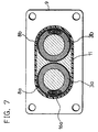
- FIG. 7 is a sectional view taken on the line VII-VII of FIG. 6. As seen in FIG. 7, the coil portions 3a and 3b are accommodated in the respective conductive members 8a and 8b so as to keep intimate contact with the interior walls of the respective conductive members 8a and 8b.
- the conductive layers 34a and 34b formed of a relatively soft metal on the outer peripheries of the coil portions 3a and 3b provide sufficient contact with the interior walls of the conductive members 8a and 8b by virtue of the softness of the conductive layers, thereby establishing good electric connection with the conductive members.
- the conductive members 8a and 8b along with the conductive layers 34a and 34b of the coil portions 3a and 3b are electrically connected to the grounding plates 9 at the terminal regions 3c and 3d by means of the conductive member 14 such as solder.
- the conductive member 14 such as solder.
- the cylindrical conductive members 8a and 8b accommodating the coil portions 3a and 3b, respectively, are housed in the resin casings 16a and 16b so that the insulating resin material 11 is molded to the coil portions and conductive members in a similar manner to the first embodiment.
- the high voltage noise filter according to the second embodiment was subjected to a test.
- a high AC voltage was applied across the fastening tabs 7a and 7b and the grounding plates 9, respectively, by means of the high voltage generating device 15 for measurement of the insulation breakdown voltage of the coatings 33a and 33b of the coated wires 29a and 29b.
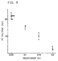
- FIG. 8 graphically represents the measurement results.
- an electric resistance was plotted as abscissa, the electric resistance measured by means of electric resistance meters 26 connected, as shown in FIG. 6, across the grounding plate 9 and the terminal regions 1e and 1f of the coil portions 3a and 3b.
- the first embodiment presented the electric resistance of from 0.15 to 0.2 ⁇ whereas the second embodiment presented much smaller electric resistance of from 0.05 to 0.1 ⁇ . This is because the conductive layers 34a and 34b of the coil portions 3a and 3b contact the interior walls of the cylindrical conductive members 8a and 8b at multiple contacting portions.
- the voltages of the high voltage generating device 15 was plotted as ordinate. The measurement results indicate that the insulation breakdown occurred at voltages of from 11 to 16 kV in the first embodiment, whereas the insulation breakdown occurred at voltages of from 17 to 22 kV in the second embodiment.
- the second embodiment has achieved much greater improvement in the withstand voltage characteristics than the first embodiment.
- the smaller electric resistance means the greater improvement in the withstand voltage characteristics. This holds for the following reason.
- the potential of the conductive layers 34a and 34b decrease with reduction of the electric resistance due to contact between the conductive layers 34a and 34b formed of a soft metal and the interior walls of the conductive members 8a and 8b at multiple contacting portions.
- the decreased potential of the conductive layers also results in decrease in the potential of the terminal regions 1e and 1f which tend to produce the electric field concentration. This further leads to the reduction of the electric field concentration, resulting in the improvement of the withstand voltage characteristics.
- FIG. 9 is a sectional view of a magnetron device incorporating a high voltage noise filter 25 of the first embodiment of the invention.
- a magnetron 13 comprises a spiral cathode 17 such as formed of thoriated-tungsten, a cylindrical anode 18 such as formed of copper, a pair of pole pieces 19a and 19b formed of a magnetic material such as iron, a ceramic support 20, an antenna 21 for emission of microwave, and a stem 22 including stem terminals 5a and 5b.
- an external magnetic circuit portion including permanent magnets 23a and 23b for producing a magnetic field externally of the magnetron portion 13, and yokes 24.
- the yokes 24 are provided with a filter case 10 such as formed of a conductive material.
- the filter case 10 accommodates the high voltage noise filter 25 according to the first embodiment.
- the high voltage noise filter 25 has the conductive wires 2a and 2b connected with the stem terminals 5a and 5b, respectively.
- FIG. 9 is a sectional view, showing only one of the two choke coils 4a and 4b and coil portions 3a and 3b which are vertically disposed with respect to the plane of the figure.
- the high voltage noise filter 25 of the first embodiment may be replaced by that of the second embodiment.
Abstract
Description
- The present invention relates to a high voltage noise filter for use in microwave devices and a magnetron device incorporating such a high voltage noise filter.
- FIG. 10 is a bottom end view illustrating a relevant portion of a magnetron incorporating a conventional high
voltage noise filter 1. In the figure,stem terminals 5a and 5b are connected withconductive wires respective stem terminals 5a and 5b of the magnetron. Theconductive wires end portions respective stem terminals 5a and 5b. At coil portions definingchoke coils conductive wires insulating layers 1a and 1b. At theother coil portions conductive wires conductive layers insulating layers 1a and 1b. Theconductive wires insulating layers 1a and 1b atend portions coil portions microwave source 6. Thecoil portions conductive members conductive layers conductive members coil portions conductive members conductive members coil portions conductive members resin casings resin casings conductive members coil portions terminal portions fastening tabs terminal portions insulating resin material 11. Theconductive members filter casing 10 by way ofgrounding plates 9. - In the high voltage noise filter of such a construction, the
insulating layers 1a and 1b formed on the outer peripheral surfaces of theconductive wires terminal regions coil portions conductive layers insulating layers 1a and 1b of theconductive materials insulating layers 1a and 1b to have an extreme thickness. An increased thickness of theinsulating layers 1a and 1b leads to an increased size of thecoil portions coil portions conductive wires - In view of the foregoing, the present invention is directed to relaxation of concentration of the aforesaid electric field in the vicinity of the end portions of the conductive layers without increasing the thickness of the
insulating layers 1a and 1b thereby improving the withstand voltage characteristics of the high voltage noise filter. The present invention has been made through experimental study and development after many experiments on examples. - A high voltage noise filter in accordance with the invention comprises a coil-shaped conductive wire for producing an inductive component, an insulating layer for producing a capacitance component formed on the surface of the conductive wire, and a conductive layer formed on at least a part of the insulating layer by means of spraying or depositing a metal material. The capacitance component is produced by the conductive wire, insulating layer and conductive layer.
- The high voltage noise filter further comprises a high withstand voltage layer comprising either a semiconductive layer or an insulative member layer, and the high withstand voltage layer is formed at least in the vicinity of an end portion of the conductive layer as interposed between the outer peripheral surface of the insulating layer and the conductive layer.
- This reduces the electric field concentration in the vicinity of the end portion of the conductive layer. As a result, the insulating layer is improved in the withstand voltage characteristics thereof for enhancing the reliability. In addition, the insulating layer can be reduced in thickness, thus providing a high voltage noise filter of small size at low costs.
- In another aspect of the high voltage noise filter in accordance with the invention, the coil-shaped conductive wire comprising the conductive layer is accommodated in a cylindrical conductive member.
- By virtue of the accommodation of the coil-shaped conductive wire in the cylindrical conductive member, the conductive layer formed on the outer periphery of the insulating layer is in contact with the interior wall of the cylindrical conductive member, defining multiple contacting portions therewith. As a result, the conductive layer and a grounding plate are connected with each other at a low resistance thorough the cylindrical conductive member electrically connected to the grounding plate, a potential of the conductive layer lowers and the electric field concentration in the vicinity of the end portion of the conductive layer is further relaxed. Therefore the insulating layer of the coil-shaped conductive wire is notably improved in the withstand voltage characteristics, resulting in an enhanced reliability.
- In yet another aspect of the high voltage noise filter in accordance with the invention, the aforesaid semiconductive layer comprises a material ranging from 10-4 to 106 Ωm in electric resistivity.
- The electric field strength in the vicinity of the end portion of the conductive layer is reduced by employing the semiconductive layer ranging from 10-4 to 106 Ωm in electric resistivity as the high withstand voltage layer.
- In yet another aspect of the high voltage noise filter in accordance with the invention, the aforesaid insulative member comprises a polyimide resin material.
- The electric field strength in the vicinity of the end portion of the conductive layer is reduced by forming the high withstand voltage layer of the polyimide resin material.
- In still another aspect of the high voltage noise filter in accordance with the invention, the aforesaid insulative member comprises a silicone resin material.
- The electric field strength in the vicinity of the end portion of the conductive layer is reduced by forming the high withstand voltage layer of the silicone resin material.
- A magnetron device in accordance with the invention incorporates a high voltage noise filter comprising a coil-shaped conductive wire for producing an inductive component, an insulating layer for producing a capacitance component formed on the surface of the conductive wire, a conductive layer partially formed on the insulating layer, and a high withstand voltage layer comprising either a semiconductive layer or an insulative member layer formed at least in the vicinity of an end portion of the conductive layer as interposed between the outer peripheral surface of the insulating layer and the conductive layer.
- The magnetron device of the invention is improved in reliability because of the incorporation of the high voltage noise filter improved in the withstand voltage characteristics, the noise filter characterized by the high withstand voltage layer formed in the vicinity of the end portion of the conductive layer of the coil-shaped conductive wire as interposed between the outer peripheral surface of the insulating layer and the conductive layer.
- In another aspect of the magnetron device in accordance with the invention, a magnetron device incorporates a high voltage noise filter wherein the coil-shaped conducive wire having the insulating layer and conductive layer is accommodated in a cylindrical conductive member.
- The high voltage noise filter can achieve a significant improvement in the withstand voltage characteristics by way of accommodation of the coil-shaped conductive wire in the cylindrical conductive member and hence, the magnetron device incorporating such a high voltage noise filter is notably improved in the reliability.
-
- FIG. 1 is a top plan view illustrating a relevant portion of a high voltage noise filter in accordance with a first embodiment of the invention;
- FIG. 2A is a top plan view illustrating a coil portion of the high voltage noise filter of the invention;
- FIG. 2B is a sectional view taken on the line b-b of FIG. 2A;
- FIG. 2C is a sectional view taken on the line c-c of FIG. 2A;
- FIG. 3A is a sectional view illustrating a wire material for the high voltage noise filter of the invention;
- FIG. 3B is a sectional view illustrating the wire material for the conventional high voltage noise filter;
- FIG. 4 is a graphical representation of the distribution of field strengths of the respective outer peripheral surfaces of the wire materials shown in FIG. 3A and FIG. 3B;
- FIG. 5 is a graphical representation of the electric strength characteristics of the high voltage noise filter of the invention and the conventional high voltage noise filter;
- FIG. 6 is a top plan view illustrating a relevant portion of a high voltage noise filter in accordance with a second embodiment hereof;
- FIG. 7 is a sectional view taken on the line VII-VII of FIG. 6;
- FIG. 8 is a graphical representation of the relationship between an electric resistance and a withstand voltage of the high voltage noise filter of the invention;
- FIG. 9 is a front view in section illustrating a magnetron device in accordance with a third embodiment hereof, the device incorporating the high voltage noise filter of the invention;
- FIG. 10 is the sectional view illustrating the relevant portion of the magnetron device incorporating the conventional high voltage noise filter.
- Preferred embodiments of the invention will be described in detail with reference to FIG. 1 through FIG. 9.
- FIG. 1 is a top plan view illustrating a high voltage noise filter in accordance with a first embodiment of the invention. In the figure,
conductive wires conductive wires conductive wires coated wires coated wires coils 10 to 20 mm in outer diameter. The choke coils 4a and 4b receivecores -
Coil portions terminal portions coil portions coated wires conductive layers conductive layers coated wires conductive layers conductive wires coatings conductive layers - FIG. 2A is a side elevation view of the
coil portion 3b shown in FIG. 1. Thecoil portion 3a has the same shape and size as thecoil portion 3b except for that thecoil portion 3a was wound in the opposite direction (in a symmetrical form) to thecoil portion 3b. Accordingly, description on FIG. 2A through FIG. 2C illustrating thecoil portion 3b is similarly applicable to thecoil portion 3a. Therefore, FIG. 2A through FIG. 2C give reference marks of the components of thecoil portion 3a accompanied by corresponding reference marks of those of thecoil portion 3b. - FIG. 2B is a sectional view of
terminal portions boundary regions coated wires terminal portions conductive wires coatings coatings voltage layers - FIG. 2C is a sectional view of
terminal regions terminal regions coatings conductive wires voltage layers conductive layers - Across the
boundary portions terminal portions terminal regions coil portions voltage layers coatings coated wires - The high withstand
voltage layers coatings coated wires voltage layers voltage layers - At the
terminal regions terminal portions coil portions conductive layers voltage layers coatings coated wires voltage layers conductive layers voltage layers boundary regions coil portions fastening tabs 71 and 7b, respectively. Similarly to theterminal regions terminal regions coil portions coatings voltage layers conductive layers - In FIG. 1, the
conductive layers terminal portions coil portions plates 9 by means ofconductive members 14 such as of solder. Thecoil portions resin casing 16a shown by sectional form in FIG. 1. Theboundary regions coil portions resin casing 16b also shown by sectional form in FIG. 1.Terminals coil portions respective fastening tabs resin casing 16b to project outward of thecasing 16b. The interior of theresin casings resin material 11, such as an epoxy resin. Consequently, portions from theterminal portions terminals fastening tabs resin 11. - According to the present invention, the
terminal regions coil portions terminal regions - FIG. 4 shows the results of a comparison between a
wire material 40 of FIG. 3A according to the invention and aconventional wire material 41 of FIG. 3B having the double-layered structure. The wire materials extended in straight lines. Thewire material 40 is used for the invention wherein thecoil portions terminal regions 1e. In thewire material 40 of FIG. 3A, a 0.3 mmthick fluororesin coating 33a is formed on the outer periphery of a copperconductive material 2a having a diameter of 1.4 mm. On the outer periphery of thecoating 33a, a 0.2 mmthick polyimide film 42 is formed as the high withstandvoltage layer 35a within a range of 20 mm along the length of the wire with a central line P extending through the middle of the 20 mm range. In addition, a 0.1 mm thick solder layer is formed as theconductive layer 34a in a region extending rightward of the central line P. The test produced a favorable result that a polyimide film of about 20 mm length contributes to improve withstand voltage characteristics of the insulative layer. - On the other hand, the
conventional wire material 41 shown in FIG. 3B comprises theconductive layer 34a formed in the region rightward of the central line P, but does not include thepolyimide film 42 as the high withstand voltage layer. The other parts of thewire material 41 are fabricated in the same manner as those of thewire material 40 shown in FIG. 3A. - As to the
wire materials coating 33a was calculated by way of the finite-element method on the assumption that an AC voltage of from 3000 to 7000 V was applied across theconductive material 2a and theconductive layer 34a. FIG. 4 graphically represents the calculation results. In FIG. 4, the numerals on the abscissa indicate the lateral distances along thewire materials wire material 40 of the invention shown by the solid line in FIG. 4 presents a field strength of about 4600 V/m for the central point P and a field strength of about 3100 V/m forlateral points 30 mm from the central point P. In contrast, theconventional wire material 41 shown by the dot-and-dash line presents a field strength of about 7000 V/m for the central point P and a field strength of about 3200 V/m forlateral points 30 mm from the central point P, which 3200 V/m does not give a significant difference from the corresponding field strength of thewire material 40. As apparent from the graph, the field strength in the vicinity of the central point P where the field strength reaches the peak value is much smaller in thewire material 40 of the invention than in theconventional wire material 41. It is to be understood that thewire material 40 of the invention notably reduces the electric field concentration. - The following test was conducted on the high voltage noise filter according to the embodiment hereof shown in FIG. 1. The
conductive wires coatings voltage layers conductive layers voltage generating device 15 was connected across thefastening tabs grounding plates 9 for applying AC voltage of from 5 kV to 18 kV. The test was conducted on the basis of ten samples, each ten samples including, as the high withstandvoltage layers coatings voltage layers - FIG. 6 is a top plan view of a high voltage noise filter according to a second embodiment hereof. In FIG. 6, the choke coils 4a and 4b and
coil portions coil portions conductive members coil portions conductive members conductive members conductive layers coil portions conductive members conductive members conductive layers coil portions grounding plates 9 at theterminal regions conductive member 14 such as solder. As seen in FIG. 6 and FIG. 7, the cylindricalconductive members coil portions resin casings resin material 11 is molded to the coil portions and conductive members in a similar manner to the first embodiment. - Similarly to the first embodiment hereof, the high voltage noise filter according to the second embodiment was subjected to a test. A high AC voltage was applied across the
fastening tabs grounding plates 9, respectively, by means of the highvoltage generating device 15 for measurement of the insulation breakdown voltage of thecoatings coated wires electric resistance meters 26 connected, as shown in FIG. 6, across thegrounding plate 9 and theterminal regions coil portions conductive layers coil portions conductive members voltage generating device 15 was plotted as ordinate. The measurement results indicate that the insulation breakdown occurred at voltages of from 11 to 16 kV in the first embodiment, whereas the insulation breakdown occurred at voltages of from 17 to 22 kV in the second embodiment. Thus, the second embodiment has achieved much greater improvement in the withstand voltage characteristics than the first embodiment. The smaller electric resistance means the greater improvement in the withstand voltage characteristics. This holds for the following reason. The potential of theconductive layers conductive layers conductive members terminal regions - A third embodiment is shown in FIG. 9, which is a sectional view of a magnetron device incorporating a high
voltage noise filter 25 of the first embodiment of the invention. In the magnetron device of this embodiment, amagnetron 13 comprises aspiral cathode 17 such as formed of thoriated-tungsten, acylindrical anode 18 such as formed of copper, a pair ofpole pieces ceramic support 20, anantenna 21 for emission of microwave, and astem 22 includingstem terminals 5a and 5b. There is further provided an external magnetic circuit portion includingpermanent magnets magnetron portion 13, and yokes 24. Theyokes 24 are provided with afilter case 10 such as formed of a conductive material. Thefilter case 10 accommodates the highvoltage noise filter 25 according to the first embodiment. The highvoltage noise filter 25 has theconductive wires stem terminals 5a and 5b, respectively. FIG. 9 is a sectional view, showing only one of the twochoke coils coil portions voltage noise filter 25 of the first embodiment may be replaced by that of the second embodiment. By employment of the high voltage noise filter of the first or second embodiment featuring excellent withstand voltage characteristics, the magnetron device according to the embodiment hereof can accomplish excellent withstand voltage characteristics and a long service life. - Although the present invention has been described in terms of the presently preferred embodiments, it is to be understood that such disclosure is not to be interpreted as limiting. Various alterations and modifications will no doubt become apparent to those skilled in the art to which the present invention pertains, after having read the above disclosure. Accordingly, it is intended that the appended claims be interpreted as covering all alterations and modifications as fall within the true spirit and scope of the invention.
Claims (7)
the coil-shaped conductive wire (3a, 3b) having said insulating layer (33a, 33b) and said conductive layer (34a, 34b) is secured by accommodation in a cylindrical conductive member (8a, 8b). (FIG. 6)
said semiconductive material (35a, 35b) has an electric resistivity of from 10-4 to 106 Ωm.
said insulative member (35a, 35b) comprises a polyimide resin material.
said insulative member (35a, 35b) comprises a silicone resin material.
the coil-shaped conductive wire (3a, 3b) having said insulating layer (33a, 33b) and conductive layer is accommodated in a cylindrical conductive member (8a, 8b). (FIG. 9)
Applications Claiming Priority (3)
| Application Number | Priority Date | Filing Date | Title |
|---|---|---|---|
| JP07291596A JP3193976B2 (en) | 1996-03-27 | 1996-03-27 | High voltage noise filter and magnetron device |
| JP7291596 | 1996-03-27 | ||
| JP72915/96 | 1996-03-27 |
Publications (3)
| Publication Number | Publication Date |
|---|---|
| EP0798950A2 true EP0798950A2 (en) | 1997-10-01 |
| EP0798950A3 EP0798950A3 (en) | 1998-12-02 |
| EP0798950B1 EP0798950B1 (en) | 2003-08-27 |
Family
ID=13503134
Family Applications (1)
| Application Number | Title | Priority Date | Filing Date |
|---|---|---|---|
| EP97104923A Expired - Lifetime EP0798950B1 (en) | 1996-03-27 | 1997-03-22 | High voltage noise filter and magnetron device using it |
Country Status (6)
| Country | Link |
|---|---|
| US (1) | US5977713A (en) |
| EP (1) | EP0798950B1 (en) |
| JP (1) | JP3193976B2 (en) |
| KR (1) | KR100241295B1 (en) |
| CN (1) | CN1075228C (en) |
| DE (1) | DE69724316T2 (en) |
Cited By (1)
| Publication number | Priority date | Publication date | Assignee | Title |
|---|---|---|---|---|
| FR2779268A1 (en) * | 1998-05-27 | 1999-12-03 | Alsthom Cge Alcatel | ELECTRIC WINDING, TRANSFORMER AND ELECTRIC MOTOR HAVING SUCH A WINDING |
Families Citing this family (8)
| Publication number | Priority date | Publication date | Assignee | Title |
|---|---|---|---|---|
| JP2002343263A (en) * | 2001-05-22 | 2002-11-29 | Sanyo Electric Co Ltd | Magnetron |
| KR100436149B1 (en) | 2001-12-24 | 2004-06-14 | 삼성전자주식회사 | Microwave oven |
| KR100419204B1 (en) | 2001-12-24 | 2004-02-21 | 삼성전자주식회사 | Microwave oven |
| JP2005209539A (en) * | 2004-01-23 | 2005-08-04 | Matsushita Electric Ind Co Ltd | Magnetron |
| JP2007095452A (en) | 2005-09-28 | 2007-04-12 | Seiko Epson Corp | Light emitting device |
| JP2007096645A (en) | 2005-09-28 | 2007-04-12 | Seiko Epson Corp | Microwave generating device and equipment using same |
| KR101898294B1 (en) * | 2012-08-13 | 2018-09-12 | 현대모비스 주식회사 | Common mode noise filter |
| KR20150022163A (en) * | 2013-08-22 | 2015-03-04 | 삼성디스플레이 주식회사 | Strap for plasma processing apparatus and plasma processing apparatus having the same |
Citations (4)
| Publication number | Priority date | Publication date | Assignee | Title |
|---|---|---|---|---|
| GB1372476A (en) * | 1971-06-03 | 1974-10-30 | Trefimetaux G P | Cables insulated with polyethylene for high voltage direct current |
| JPS571214A (en) * | 1979-11-12 | 1982-01-06 | Toyo Electric Mfg Co Ltd | Manufacture of coil for electric apparatus using corona preventive film |
| EP0440865A1 (en) * | 1990-02-09 | 1991-08-14 | Asea Brown Boveri Ab | Electrical insulation |
| EP0696878A2 (en) * | 1994-08-09 | 1996-02-14 | Matsushita Electric Industrial Co., Ltd. | Microwave apparatus |
Family Cites Families (10)
| Publication number | Priority date | Publication date | Assignee | Title |
|---|---|---|---|---|
| US2841771A (en) * | 1951-04-18 | 1958-07-01 | Frank S Dunleavey | Four-terminal filter embodying an ionized medium |
| DE2125100C3 (en) * | 1970-05-20 | 1973-11-15 | Hitachi Cable Ltd. | Megnetron |
| US3727098A (en) * | 1971-07-22 | 1973-04-10 | Litton Systems Inc | Magnetron filter box |
| JPS5546623B2 (en) * | 1972-09-01 | 1980-11-25 | ||
| JPS5577370A (en) * | 1978-12-04 | 1980-06-11 | Nissin Electric Co Ltd | Harmonic filter |
| JPH05275958A (en) * | 1992-03-25 | 1993-10-22 | Murata Mfg Co Ltd | Noise filter |
| JPH06112752A (en) * | 1992-09-25 | 1994-04-22 | Tdk Corp | High voltage noise filter and magnetron |
| JP3453787B2 (en) * | 1993-06-18 | 2003-10-06 | ソニー株式会社 | Semiconductor laser and manufacturing method thereof |
| JPH0715127A (en) * | 1993-06-24 | 1995-01-17 | Hitachi Denshi Ltd | Inspection method of detecting foreign material to soldering printed circuit board |
| JP4091412B2 (en) * | 2002-12-06 | 2008-05-28 | 三星電子株式会社 | Despreading method in wireless communication |
-
1996
- 1996-03-27 JP JP07291596A patent/JP3193976B2/en not_active Expired - Fee Related
-
1997
- 1997-03-22 EP EP97104923A patent/EP0798950B1/en not_active Expired - Lifetime
- 1997-03-22 DE DE69724316T patent/DE69724316T2/en not_active Expired - Fee Related
- 1997-03-26 US US08/827,079 patent/US5977713A/en not_active Expired - Fee Related
- 1997-03-27 CN CN97109943A patent/CN1075228C/en not_active Expired - Fee Related
- 1997-03-27 KR KR1019970010759A patent/KR100241295B1/en not_active IP Right Cessation
Patent Citations (4)
| Publication number | Priority date | Publication date | Assignee | Title |
|---|---|---|---|---|
| GB1372476A (en) * | 1971-06-03 | 1974-10-30 | Trefimetaux G P | Cables insulated with polyethylene for high voltage direct current |
| JPS571214A (en) * | 1979-11-12 | 1982-01-06 | Toyo Electric Mfg Co Ltd | Manufacture of coil for electric apparatus using corona preventive film |
| EP0440865A1 (en) * | 1990-02-09 | 1991-08-14 | Asea Brown Boveri Ab | Electrical insulation |
| EP0696878A2 (en) * | 1994-08-09 | 1996-02-14 | Matsushita Electric Industrial Co., Ltd. | Microwave apparatus |
Non-Patent Citations (1)
| Title |
|---|
| PATENT ABSTRACTS OF JAPAN vol. 006, no. 060 (E-102), 17 April 1982 & JP 57 001214 A (TOYO ELECTRIC MFG CO LTD), 6 January 1982 * |
Cited By (2)
| Publication number | Priority date | Publication date | Assignee | Title |
|---|---|---|---|---|
| FR2779268A1 (en) * | 1998-05-27 | 1999-12-03 | Alsthom Cge Alcatel | ELECTRIC WINDING, TRANSFORMER AND ELECTRIC MOTOR HAVING SUCH A WINDING |
| US6287691B1 (en) | 1998-05-27 | 2001-09-11 | Nexans | Electrical winding, and a transformer and an electric motor including such a winding |
Also Published As
| Publication number | Publication date |
|---|---|
| CN1075228C (en) | 2001-11-21 |
| DE69724316D1 (en) | 2003-10-02 |
| EP0798950B1 (en) | 2003-08-27 |
| JPH09265914A (en) | 1997-10-07 |
| DE69724316T2 (en) | 2004-06-09 |
| KR970067492A (en) | 1997-10-13 |
| EP0798950A3 (en) | 1998-12-02 |
| KR100241295B1 (en) | 2000-02-01 |
| US5977713A (en) | 1999-11-02 |
| JP3193976B2 (en) | 2001-07-30 |
| CN1169062A (en) | 1997-12-31 |
Similar Documents
| Publication | Publication Date | Title |
|---|---|---|
| WO2004036601A2 (en) | Highly insulated inductive data couplers | |
| EP1966806A1 (en) | High voltage bushing and high voltage device comprising such bushing | |
| US5977713A (en) | High voltage noise filter and magnetron device using it | |
| JP3473795B2 (en) | High voltage capacitors and magnetrons | |
| EP2057641A1 (en) | High voltage bushing | |
| US5844366A (en) | Magnetron coiled feedthrough LC filter | |
| US3835370A (en) | Dampened choke coil | |
| US3295055A (en) | Combined unit of impedance | |
| US3259857A (en) | Conductor having distributed capacitance | |
| CN113488321B (en) | Dry-type transformer and winding method thereof | |
| JPS5930522Y2 (en) | High voltage feed-through capacitor | |
| JPH0624991Y2 (en) | Gas insulated transformer | |
| KR820002492Y1 (en) | Electrical composite part | |
| CN117079949A (en) | Shielding device and electrical equipment | |
| JP2540132Y2 (en) | Winding structure of gas-insulated electrical equipment | |
| JP3460702B2 (en) | Transformers for gas insulated instruments | |
| EP0286980A1 (en) | High-voltage transformer | |
| JPS5943717Y2 (en) | Feedthrough capacitor | |
| JP2607629Y2 (en) | Feed-through capacitor | |
| JPH04261003A (en) | Insulation structure of electronic device | |
| JPS5936902Y2 (en) | High voltage LC composite parts | |
| JPS59204217A (en) | Transformer | |
| KR19980028930U (en) | Chip coil | |
| JPS6151709A (en) | Dc insulated conductor | |
| JP2002373821A (en) | Transformer for gas-insulated instrument |
Legal Events
| Date | Code | Title | Description |
|---|---|---|---|
| PUAI | Public reference made under article 153(3) epc to a published international application that has entered the european phase |
Free format text: ORIGINAL CODE: 0009012 |
|
| AK | Designated contracting states |
Kind code of ref document: A2 Designated state(s): DE FR GB |
|
| PUAL | Search report despatched |
Free format text: ORIGINAL CODE: 0009013 |
|
| AK | Designated contracting states |
Kind code of ref document: A3 Designated state(s): DE FR GB |
|
| 17P | Request for examination filed |
Effective date: 19990226 |
|
| RAP1 | Party data changed (applicant data changed or rights of an application transferred) |
Owner name: MATSUSHITA ELECTRIC INDUSTRIAL CO., LTD. |
|
| RAP1 | Party data changed (applicant data changed or rights of an application transferred) |
Owner name: MATSUSHITA ELECTRIC INDUSTRIAL CO., LTD. |
|
| 17Q | First examination report despatched |
Effective date: 20020522 |
|
| GRAH | Despatch of communication of intention to grant a patent |
Free format text: ORIGINAL CODE: EPIDOS IGRA |
|
| GRAS | Grant fee paid |
Free format text: ORIGINAL CODE: EPIDOSNIGR3 |
|
| GRAA | (expected) grant |
Free format text: ORIGINAL CODE: 0009210 |
|
| AK | Designated contracting states |
Designated state(s): DE FR GB |
|
| REG | Reference to a national code |
Ref country code: GB Ref legal event code: FG4D |
|
| REF | Corresponds to: |
Ref document number: 69724316 Country of ref document: DE Date of ref document: 20031002 Kind code of ref document: P |
|
| ET | Fr: translation filed | ||
| PLBE | No opposition filed within time limit |
Free format text: ORIGINAL CODE: 0009261 |
|
| STAA | Information on the status of an ep patent application or granted ep patent |
Free format text: STATUS: NO OPPOSITION FILED WITHIN TIME LIMIT |
|
| 26N | No opposition filed |
Effective date: 20040528 |
|
| PGFP | Annual fee paid to national office [announced via postgrant information from national office to epo] |
Ref country code: FR Payment date: 20060308 Year of fee payment: 10 |
|
| PGFP | Annual fee paid to national office [announced via postgrant information from national office to epo] |
Ref country code: DE Payment date: 20060316 Year of fee payment: 10 |
|
| GBPC | Gb: european patent ceased through non-payment of renewal fee |
Effective date: 20070322 |
|
| REG | Reference to a national code |
Ref country code: FR Ref legal event code: ST Effective date: 20071130 |
|
| PG25 | Lapsed in a contracting state [announced via postgrant information from national office to epo] |
Ref country code: DE Free format text: LAPSE BECAUSE OF NON-PAYMENT OF DUE FEES Effective date: 20071002 |
|
| PG25 | Lapsed in a contracting state [announced via postgrant information from national office to epo] |
Ref country code: GB Free format text: LAPSE BECAUSE OF NON-PAYMENT OF DUE FEES Effective date: 20070322 |
|
| PG25 | Lapsed in a contracting state [announced via postgrant information from national office to epo] |
Ref country code: FR Free format text: LAPSE BECAUSE OF NON-PAYMENT OF DUE FEES Effective date: 20070402 |
|
| PGFP | Annual fee paid to national office [announced via postgrant information from national office to epo] |
Ref country code: GB Payment date: 20060322 Year of fee payment: 10 |