EP0798403A1 - Continuously charged czochralski method of manufacturing silicon monocrystal, and dopant feeding apparatus - Google Patents
Continuously charged czochralski method of manufacturing silicon monocrystal, and dopant feeding apparatus Download PDFInfo
- Publication number
- EP0798403A1 EP0798403A1 EP97302063A EP97302063A EP0798403A1 EP 0798403 A1 EP0798403 A1 EP 0798403A1 EP 97302063 A EP97302063 A EP 97302063A EP 97302063 A EP97302063 A EP 97302063A EP 0798403 A1 EP0798403 A1 EP 0798403A1
- Authority
- EP
- European Patent Office
- Prior art keywords
- dopant
- silicon
- crucible
- silicon melt
- monocrystal
- Prior art date
- Legal status (The legal status is an assumption and is not a legal conclusion. Google has not performed a legal analysis and makes no representation as to the accuracy of the status listed.)
- Withdrawn
Links
- XUIMIQQOPSSXEZ-UHFFFAOYSA-N Silicon Chemical compound [Si] XUIMIQQOPSSXEZ-UHFFFAOYSA-N 0.000 title claims abstract description 206
- 229910052710 silicon Inorganic materials 0.000 title claims abstract description 206
- 239000010703 silicon Substances 0.000 title claims abstract description 206
- 239000002019 doping agent Substances 0.000 title claims abstract description 153
- 238000004519 manufacturing process Methods 0.000 title claims description 18
- 239000002210 silicon-based material Substances 0.000 claims abstract description 30
- 238000005204 segregation Methods 0.000 claims abstract description 29
- 238000000034 method Methods 0.000 claims abstract description 22
- 239000011148 porous material Substances 0.000 claims abstract description 6
- 238000003860 storage Methods 0.000 claims description 4
- 238000007599 discharging Methods 0.000 claims 1
- 230000007423 decrease Effects 0.000 description 6
- 238000009826 distribution Methods 0.000 description 4
- 238000005259 measurement Methods 0.000 description 4
- ZOXJGFHDIHLPTG-UHFFFAOYSA-N Boron Chemical compound [B] ZOXJGFHDIHLPTG-UHFFFAOYSA-N 0.000 description 3
- OKTJSMMVPCPJKN-UHFFFAOYSA-N Carbon Chemical compound [C] OKTJSMMVPCPJKN-UHFFFAOYSA-N 0.000 description 3
- 229910052796 boron Inorganic materials 0.000 description 3
- 229910002804 graphite Inorganic materials 0.000 description 3
- 239000010439 graphite Substances 0.000 description 3
- 239000000203 mixture Substances 0.000 description 2
- 230000003252 repetitive effect Effects 0.000 description 2
- -1 0.75 Chemical compound 0.000 description 1
- 229910052787 antimony Inorganic materials 0.000 description 1
- WATWJIUSRGPENY-UHFFFAOYSA-N antimony atom Chemical compound [Sb] WATWJIUSRGPENY-UHFFFAOYSA-N 0.000 description 1
- 230000003247 decreasing effect Effects 0.000 description 1
- 230000001419 dependent effect Effects 0.000 description 1
- BHEPBYXIRTUNPN-UHFFFAOYSA-N hydridophosphorus(.) (triplet) Chemical compound [PH] BHEPBYXIRTUNPN-UHFFFAOYSA-N 0.000 description 1
- 239000000463 material Substances 0.000 description 1
Images


Classifications
-
- C—CHEMISTRY; METALLURGY
- C30—CRYSTAL GROWTH
- C30B—SINGLE-CRYSTAL GROWTH; UNIDIRECTIONAL SOLIDIFICATION OF EUTECTIC MATERIAL OR UNIDIRECTIONAL DEMIXING OF EUTECTOID MATERIAL; REFINING BY ZONE-MELTING OF MATERIAL; PRODUCTION OF A HOMOGENEOUS POLYCRYSTALLINE MATERIAL WITH DEFINED STRUCTURE; SINGLE CRYSTALS OR HOMOGENEOUS POLYCRYSTALLINE MATERIAL WITH DEFINED STRUCTURE; AFTER-TREATMENT OF SINGLE CRYSTALS OR A HOMOGENEOUS POLYCRYSTALLINE MATERIAL WITH DEFINED STRUCTURE; APPARATUS THEREFOR
- C30B15/00—Single-crystal growth by pulling from a melt, e.g. Czochralski method
- C30B15/02—Single-crystal growth by pulling from a melt, e.g. Czochralski method adding crystallising materials or reactants forming it in situ to the melt
- C30B15/04—Single-crystal growth by pulling from a melt, e.g. Czochralski method adding crystallising materials or reactants forming it in situ to the melt adding doping materials, e.g. for n-p-junction
-
- Y—GENERAL TAGGING OF NEW TECHNOLOGICAL DEVELOPMENTS; GENERAL TAGGING OF CROSS-SECTIONAL TECHNOLOGIES SPANNING OVER SEVERAL SECTIONS OF THE IPC; TECHNICAL SUBJECTS COVERED BY FORMER USPC CROSS-REFERENCE ART COLLECTIONS [XRACs] AND DIGESTS
- Y10—TECHNICAL SUBJECTS COVERED BY FORMER USPC
- Y10T—TECHNICAL SUBJECTS COVERED BY FORMER US CLASSIFICATION
- Y10T117/00—Single-crystal, oriented-crystal, and epitaxy growth processes; non-coating apparatus therefor
- Y10T117/10—Apparatus
- Y10T117/1024—Apparatus for crystallization from liquid or supercritical state
- Y10T117/1032—Seed pulling
- Y10T117/1052—Seed pulling including a sectioned crucible [e.g., double crucible, baffle]
-
- Y—GENERAL TAGGING OF NEW TECHNOLOGICAL DEVELOPMENTS; GENERAL TAGGING OF CROSS-SECTIONAL TECHNOLOGIES SPANNING OVER SEVERAL SECTIONS OF THE IPC; TECHNICAL SUBJECTS COVERED BY FORMER USPC CROSS-REFERENCE ART COLLECTIONS [XRACs] AND DIGESTS
- Y10—TECHNICAL SUBJECTS COVERED BY FORMER USPC
- Y10T—TECHNICAL SUBJECTS COVERED BY FORMER US CLASSIFICATION
- Y10T117/00—Single-crystal, oriented-crystal, and epitaxy growth processes; non-coating apparatus therefor
- Y10T117/10—Apparatus
- Y10T117/1024—Apparatus for crystallization from liquid or supercritical state
- Y10T117/1032—Seed pulling
- Y10T117/1056—Seed pulling including details of precursor replenishment
Definitions
- the present invention relates to an improved continuously charged Czochralski method (i.e., a CCZ method) of manufacturing a silicon monocrystal and, more particularly, to a method of manufacturing a silicon monocrystal whose resistivity is controlled so as to fall within a predetermined range. Further, the present invention relates to a dopant feeding apparatus suitable for use in the manufacturing method.
- a CCZ method continuously charged Czochralski method
- the silicon monocrystal in order to control the resistivity of a silicon monocrystal to be pulled, the silicon monocrystal is pulled while dopant; e.g., boron, phosphorous, or antimony, is added to the silicon melt. Introduction of dopant into the silicon monocrystal is dependent on segregation. As the pulling of silicon monocrystal proceeds, the dopant concentration of the remaining silicon melt increases, and, as a result, the resistivity of the silicon monocrystal to be pulled gradually decreases.
- dopant e.g., boron, phosphorous, or antimony
- the resistivity of the silicon monocrystal is determined by an exponential curve defined by an effective segregation coefficient (k eff ) of the dopant.
- effective segregation coefficient (k eff ) of the dopant is used herein to refer to a segregation coefficient when a silicon monocrystal is actually grown. For example, if the resistivity is measured at both longitudinal ends of the silicon monocrystal block, the distribution of resistivity of the area of silicon monocrystal block between its longitudinal ends can be determined from the exponential curve. Because of this, it is possible to confirm which portion of the silicon monocrystal block has a desired range of resistivity without the need of any further measurements.
- the resistivity of the silicon monocrystal to be pulled decreases exponentially for reasons of segregation, and therefore the resistivity of the latter half of the silicon monocrystal deviates from a desired range of resistivity, thereby resulting in decreased manufacturing yield.
- the silicon monocrystal is pulled while its resistivity is controlled by charging silicon material to the silicon melt whose volume reduces as a result of pulling of the silicon monocrystal, so as to prevent the dopant concentration of the silicon melt from increasing.
- the silicon material is charged so as to maintain the dopant concentration of the silicon melt constant, the resistivity of the silicon monocrystal to be pulled can be maintained constantly.
- a longer silicon monocrystal is pulled through addition of dopant as well as silicon material to the silicon melt.
- the granular silicon material and the dopant-containing granular silicon material are mixed in a suitable ratio.
- the dopant-containing granular silicon material is special material, and therefore this method is impracticable.
- a double crucible comprising an outer crucible and an inner crucible which communicate with each other through pores.
- Use of the double crucible is intended to control the resistivity of a silicon monocrystal to be pulled by continuously charging dopant to the silicon melt stored in the outer crucible, and by causing the thus-charged dopant to flow into the inner crucible through the pores. Since it is impossible to measure the resistivity of the silicon monocrystal while it is being pulled, it is impossible to control the amount of dopant to be charged to the silicon melt of the outer crucible on the basis of feedback on the resistivity of the silicon monocrystal. Therefore, the resistivity of a resultantly-obtained silicon monocrystal may deviate from a desired range.
- an object of the present invention is to provide an improved CCZ method of manufacturing a silicon monocrystal in which the resistivity of a silicon monocrystal pulled from a double crucible can be controlled within a desired range using commonly-employed dopant.
- Another object of the present invention is to provide a dopant feeding apparatus suitable for use in the improved CCZ method.
- C s (0) represents the initial resistivity of a silicon monocrystal
- C s (W) represents the resistivity of the silicon monocrystal after being grown to a weight W
- C outl (W) represents the dopant concentration of the silicon melt stored in the outer crucible
- C inl (W) represents the dopant concentration of the silicon melt stored in the inner crucible.
- the ratio of resistivity (C s (0)/C s (W)) of the silicon monocrystal to be pulled from the double crucible can be controlled so as to fall within a certain range using commonly-used dopant, so long as pulling of a silicon monocrystal is commenced in a state in which the ratio of C outl (W) to C inl (W), or C outl (W)/C inl (W) (hereinafter may be referred to as the dopant concentration ratio), is larger than an effective segregation coefficient (k eff ) of the dopant, namely, in a state in which C outl (0)/C inl (0) > k eff ; when the ratio C outl (W)/C inl (W) becomes smaller than k eff , the dopant is recharged to the silicon melt stored in the outer crucible so as to make the ratio C outl (W)/C inl (W) greater than k eff ; and this operation is repeated whenever the dopant concentration ratio becomes smaller than the effective
- the present invention provides an improved CCZ method of manufacturing a silicon monocrystal in which a silicon monocrystal is pulled while silicon material is charged to silicon melt stored in a crucible.
- the crucible is a double crucible composed of an outer crucible and an inner crucible which communicate with each other through pores. The method comprises the steps of:
- the dopant when the dopant concentration of the silicon melt stored in the inner crucible becomes equal to its initial value before commencement of pulling of the silicon monocrystal, the dopant is charged to the silicon melt of the outer crucible. More preferably, when the dopant concentration of the silicon melt stored in the inner crucible becomes equal to its initial value before commencement of pulling of the silicon monocrystal, the dopant concentration of the silicon melt stored in the outer crucible is made equal to its initial value before commencement of pulling of the silicon monocrystal by charging the dopant to the silicon melt of the outer crucible. As a result of this, it is possible to better control the range of the resistivity of the silicon monocrystal to be pulled.
- the present invention provides a dopant feeding apparatus for use with the previously-described CCZ method of manufacturing a silicon monocrystal.
- the dopant feeding apparatus comprises a plurality of dopant storage sections capable of charging dopant to silicon melt a plurality of times.
- the ratio of resistivity [i.e., C s (0)/C s (W )] of the silicon monocrystal pulled from the double crucible can be controlled within a desired range using commonly-employed dopant. Accordingly, the present invention allows a silicon monocrystal having a desired range of resistivity to be manufactured at high yield and low cost.
- reference numeral 1 denotes a double quartz-crucible
- 2 denotes an outer crucible
- 3 denotes an inner crucible.
- the double quartz-crucible 1 is supported by a graphite crucible 4 and is housed in a chamber 5.
- the outer crucible 2 and the inner crucible 3 communicate with each other through pores (not shown) formed in an interior wall 7.
- a rotary shaft 8 is attached to the graphite crucible 4, whereby the double quartz-crucible 1 and the graphite crucible 4 can rotate and are vertically movable.
- the silicon melt stored in the double quartz-crucible 1 is heated by a heater 21, or silicon material and dopant supplied to the double quartz-crucible 1 are heated by the heater 21 so as to become melted.
- the apparatus is equipped with a feed pipe 10 for introducing granular silicon material into the outer crucible 2.
- the granular silicon material is supplied to the feed pipe 10 from a feeder 6.
- the feeder 6 is capable of continuously or intermittently supplying the granular silicon material to the feed pipe 10 in a fixed or variable amount.
- the present apparatus is equipped with a dopant feeding apparatus 9 capable of feeding a predetermined amount of dopant to silicon melt a plurality of times at desired points of time.
- the silicon material is supplied to the silicon melt stored in the outer crucible via the feed pipe so as to maintain a constant amount of silicon melt in the double quartz-crucible, the pulling of the silicon monocrystal is continued.
- the dopant concentration of the silicon melt stored in the outer crucible decreases.
- the dopant concentration of the silicon melt stored in the outer crucible decreases further.
- the dopant concentration ratio becomes smaller than the effective segregation coefficient; namely, (iii) C outl (W 3 )/C inl (W 3 ) ⁇ k eff ,
- the dopant is charged to the silicon melt stored in the outer crucible using the dopant feeding apparatus so as to cause the dopant concentration ratio to again become (i') C outl (W 1' ) /C inl (W 1' ) > k eff .
- the dopant has been previously charged to the silicon melt before a silicon material is pulled. After the pulling of the silicon monocrystal has been commenced, the dopant is not charged to the silicon melt. In this state, while the granular silicon material is supplied via the feed pipe to the silicon melt stored in the outer crucible so as to maintain a constant amount of silicon melt in the double quartz-crucible, the silicon monocrystal is pulled.
- Equation (1) the relationship between the weight W of crystallized silicon and the dopant concentration C inl (W) of the silicon melt of the inner crucible obtained at the weight W is expressed by Equation (1):
- C inl (W) e -keff W inl (0) • W • [C inl (0) + W outl (0) [-W inl (0) + k eff • W outl (0)] • C outl (0) • (e keff • W outl (0) - W inl (0) W inl (0) • W outl (0) • W - 1)]
- k eff is an effective segregation coefficient
- W inl (0) is the weight of the silicon melt contained in the inner crucible when pulling of the silicon monocrystal is commenced
- W outl (0) is the weight of the silicon melt stored in the outer crucible when the pulling of the silicon monocrystal is commenced
- C inl (0) is the dopant concentration of the silicon melt stored in the inner crucible when the pulling of the silicon monoc
- FIG. 2 illustrates the relationship between the weight W of crystallized silicon and the ratio of resistivity C s (0)/C s (W) of the silicon monocrystal to be pulled obtained when the silicon monocrystal is pulled without addition of dopant after commencement of pulling of the silicon monocrystal, with regard to the respective cases where the dopant concentration ratio obtained at the time of commencement of the pulling of the silicon monocrystal, or C outl (0)/C inl (0), is 0, 0.75 (which is the k eff of boron), 2.0, and 3.0.
- C s (W) is calculated from C inl (W) obtained by Equation (1).
- C s (W) k eff X C inl (W)
- the k eff of boron namely, 0.75, is used as k eff .
- the ratio of resistivity C s (0)/C s (W) temporarily decreases so as to be smaller than one which is the value at the time of commencement of silicon monocrystal to be pulled. Then, the ratio of resistivity returns to one and further increases so as to be larger than one.
- FIG. 3 is a graph illustrating variations in C s (0)/C s (W) as a result of repetitive addition of the dopant to the silicon melt stored in the outer crucible according to the present invention, provided that the dopant concentration ratio obtained at the time of commencement of the pulling of the silicon monocrystal is 2.0.
- the ratio of resistivity C s (0)/C s (W) is controlled within a constant range by charging the dopant to the silicon melt of the outer crucible.
- the dopant concentration ratio - i.e., C outl (W 1 )/C inl (W 1 ) or C outl (W 1' )/C inl (W 1' ) - is increased so as to become larger than the effective segregation coefficient (k eff ). If this ratio is increased, the number of times that the dopant is charged per weight of crystallized silicon, will decrease. However, as illustrated in FIG. 4, the weight (W) of silicon which is crystallized until C s (0)/C s (W) returns to one; i.e., a value before commencement of pulling of the silicon monocrystal, increases. As can be seen from FIG.
- FIG. 4 is a graph illustrating the relationship between C outl (0)/C inl (0) and the weight W of silicon which is crystallized until C s (0)/C s (W) returns to one - i.e., an initial value at the time of commencement of the pulling of the silicon monocrystal; as well as the relationship between C outl (0)/C inl (0) and W at a point of inflection in a C s (0)/C s (W) curve.
- FIG. 5 is a graph illustrating the relationship between C outl (0)/C inl (0) and the reciprocal of the ratio of resistivity of the silicon monocrystal to be pulled at a point of inflection of the C s (0)/C s (W) curve; i.e., C s (W)/C s (0).
- dopant is charged to the outer crucible several times during the course of pulling of the silicon monocrystal.
- the charging of dopant to the silicon melt does not require any special dopant feeding equipment.
- a dopant feeding apparatus of any type may be used so long as it has a plurality of dopant storage sections and is capable of charging a predetermined amount of dopant to silicon melt several times at desired points in time.
- a dopant feeding apparatus 11 as provided in FIGS. 7A and 7B is used.
- the dopant feeding apparatus 11 is provided with a plurality of dopant feed pipes 13 which serve as dopant storage sections. More specifically, in the dopant feeding apparatus 11 shown in FIGS. 7A and 7B, the twelve feed pipes 13 are provided at 30° intervals around a rotary shaft 16. The lower ends of the dopant feed pipes 13 are open and in contact with a disk member 12, whereby the dopant stored in the dopant feed pipes is prevented from being discharged.
- the disk member 12 is rotatable about the rotary shaft 16. By rotation of a handle 14 mounted on the uppermost end of the rotary shaft 16, the disk member 12 can be rotated via the rotary shaft 16. One aperture 15 is formed in the disk member 12.
- the dopant feed pipes 13 may be arranged linearly. Further, although one disk member is used in the dopant feeding apparatus shown in FIGS. 7A and 7B, a member of any shape may be used so long as it is capable of preventing the dopant stored in the dopant feed pipes from being discharged. Further, the number of members is not limited to one. Further, the dopant feed pipes may be movably arranged so long as the aperture 15 formed in the disk member 12 can be brought in alignment with the open ends of the dopant feed pipes at a desired time.
- a silicon monocrystal having a diameter of 6 inches was manufactured using a CCZ method.
- the double crucible was filled with silicon melt, and dopant was charged to the outer and inner crucibles before commencement of pulling of a silicon monocrystal such that the dopant concentration of the silicon melt stored in the outer crucible became twice that of the silicon melt stored in the inner crucible. Subsequently, the pulling of a silicon monocrystal was commenced. At this time, the amount of the silicon melt stored in the double crucible was maintained constant by supplying granular silicon material to the outer crucible through the feed pipe.
- the dopant concentration of the silicon melt of the inner crucible became equal to the dopant concentration of the silicon melt of the inner crucible before the pulling of the silicon monocrystal was started; more specifically, when the weight of the crystallized silicon reached 5 kg, 23 kg, or 34 kg (or when the length of the body portion of the silicon monocrystal to be pulled reached 10 cm, 50 cm, or 75 cm), the dopant concentration of the silicon melt of the outer crucible was controlled so as to become equal to the dopant concentration of the silicon melt of the outer crucible before commencement of pulling of the silicon monocrystal, by charging the dopant to the silicon melt of the outer crucible using the dopant feeding apparatus.
- FIG. 6 illustrates results of measurement of the ratio of resistivity [that is, C s (0)/C s (W)] of the silicon monocrystal that was pulled in the test.
Landscapes
- Chemical & Material Sciences (AREA)
- Engineering & Computer Science (AREA)
- Crystallography & Structural Chemistry (AREA)
- Materials Engineering (AREA)
- Metallurgy (AREA)
- Organic Chemistry (AREA)
- Crystals, And After-Treatments Of Crystals (AREA)
- Liquid Deposition Of Substances Of Which Semiconductor Devices Are Composed (AREA)
Abstract
A silicon monocrystal is manufactured according to the continuously charged Czochralski method in which a double crucible is used which is composed of an outer crucible and an inner crucible which communicate with each other through pores. A dopant is charged to the silicon melt stored in the double crucible before commencing pulling of a silicon monocrystal such that the ratio of the dopant concentration of the silicon melt stored in the outer crucible to the dopant concentration of the silicon melt stored in the inner crucible becomes greater than an effective segregation coefficient of the dopant. The silicon monocrystal is then pulled while silicon material is charged to the silicon melt within the outer crucible, during which the dopant concentration ratio becomes equal to the effective segregation coefficient and then becomes smaller than the effective segregation coefficient. When the dopant concentration ratio becomes smaller than the effective segregation coefficient, the dopant is charged to the silicon melt stored in the outer crucible. The above operation is repeated, so that the resistivity of the silicon monocrystal pulled from the double crucible can be controlled within a desired range using commonly-employed dopant.
Description
- The present invention relates to an improved continuously charged Czochralski method (i.e., a CCZ method) of manufacturing a silicon monocrystal and, more particularly, to a method of manufacturing a silicon monocrystal whose resistivity is controlled so as to fall within a predetermined range. Further, the present invention relates to a dopant feeding apparatus suitable for use in the manufacturing method.
- There exists a CCZ method in which a silicon monocrystal is pulled while silicon material is supplied to silicon melt whose volume reduces as a result of pulling of the silicon monocrystal. This method enables the pulling of a longer silicon monocrystal from one crucible, thereby improving manufacturing yield and reducing manufacturing costs of the silicon monocrystal.
- In the ordinary CZ method, in order to control the resistivity of a silicon monocrystal to be pulled, the silicon monocrystal is pulled while dopant; e.g., boron, phosphorous, or antimony, is added to the silicon melt. Introduction of dopant into the silicon monocrystal is dependent on segregation. As the pulling of silicon monocrystal proceeds, the dopant concentration of the remaining silicon melt increases, and, as a result, the resistivity of the silicon monocrystal to be pulled gradually decreases.
- At this time, the resistivity of the silicon monocrystal is determined by an exponential curve defined by an effective segregation coefficient (keff) of the dopant. The term "effective segregation coefficient (keff) of the dopant" is used herein to refer to a segregation coefficient when a silicon monocrystal is actually grown. For example, if the resistivity is measured at both longitudinal ends of the silicon monocrystal block, the distribution of resistivity of the area of silicon monocrystal block between its longitudinal ends can be determined from the exponential curve. Because of this, it is possible to confirm which portion of the silicon monocrystal block has a desired range of resistivity without the need of any further measurements.
- However, according to the ordinary CZ Method, the resistivity of the silicon monocrystal to be pulled decreases exponentially for reasons of segregation, and therefore the resistivity of the latter half of the silicon monocrystal deviates from a desired range of resistivity, thereby resulting in decreased manufacturing yield.
- To prevent the previously-described problem, an improved CCZ method has been developed. According to this method, the silicon monocrystal is pulled while its resistivity is controlled by charging silicon material to the silicon melt whose volume reduces as a result of pulling of the silicon monocrystal, so as to prevent the dopant concentration of the silicon melt from increasing. In this method, if the silicon material is charged so as to maintain the dopant concentration of the silicon melt constant, the resistivity of the silicon monocrystal to be pulled can be maintained constantly. However, it will be impossible to pull a too long silicon monocrystal without addition of the dopant. In some cases, a longer silicon monocrystal is pulled through addition of dopant as well as silicon material to the silicon melt.
- In this case, there is a method of pulling a silicon monocrystal while charging to silicon melt a mixture of granular silicon material and dopant-containing granular silicon material that has the same shape distribution as the granular silicon material and is capable of being evenly mixed with the granular silicon material. The granular silicon material and the dopant-containing granular silicon material are mixed in a suitable ratio. The dopant-containing granular silicon material is special material, and therefore this method is impracticable.
- There is still another method of pulling a silicon monocrystal while continuously charging dopant - which is different in shape distribution from the granular silicon material and does not evenly mix with the granular silicon material - to the silicon melt separately from the granular silicon material. In this method, since the amount of dopant to be continuously charged is small, a large amount of errors arise in the amount of dopant to be added. As a result, variations in the resistivity of the silicon monocrystal to be pulled become greater. For this reason, this method is also impracticable.
- In the previously-described methods, there may be used a double crucible comprising an outer crucible and an inner crucible which communicate with each other through pores. Use of the double crucible is intended to control the resistivity of a silicon monocrystal to be pulled by continuously charging dopant to the silicon melt stored in the outer crucible, and by causing the thus-charged dopant to flow into the inner crucible through the pores. Since it is impossible to measure the resistivity of the silicon monocrystal while it is being pulled, it is impossible to control the amount of dopant to be charged to the silicon melt of the outer crucible on the basis of feedback on the resistivity of the silicon monocrystal. Therefore, the resistivity of a resultantly-obtained silicon monocrystal may deviate from a desired range.
- In contrast to the ordinary CZ method, even if the resistivity is measured at both longitudinal ends of the silicon monocrystal block, the distribution of resistivity of the area of the silicon monocrystal between its longitudinal ends cannot be determined, because the dopant is continuously charged during the course of pulling of the silicon monocrystal. Because of this, without further measurement of resistivity it is impossible to confirm which portion of the silicon monocrystal block has a desired range of resistivity.
- In view of the aforementioned drawbacks, an object of the present invention is to provide an improved CCZ method of manufacturing a silicon monocrystal in which the resistivity of a silicon monocrystal pulled from a double crucible can be controlled within a desired range using commonly-employed dopant.
- Another object of the present invention is to provide a dopant feeding apparatus suitable for use in the improved CCZ method.
- Through various studies made, the inventors of the present invention have discovered the following phenomenon with regard to a CCZ method of manufacturing a silicon monocrystal in which a silicon monocrystal is pulled while silicon material is charged to silicon melt stored in a double crucible. In this discussion, Cs(0) represents the initial resistivity of a silicon monocrystal, Cs(W) represents the resistivity of the silicon monocrystal after being grown to a weight W, Coutl(W) represents the dopant concentration of the silicon melt stored in the outer crucible, and Cinl(W) represents the dopant concentration of the silicon melt stored in the inner crucible. The ratio of resistivity (Cs(0)/Cs(W)) of the silicon monocrystal to be pulled from the double crucible can be controlled so as to fall within a certain range using commonly-used dopant, so long as pulling of a silicon monocrystal is commenced in a state in which the ratio of Coutl(W) to Cinl(W), or Coutl(W)/Cinl(W) (hereinafter may be referred to as the dopant concentration ratio), is larger than an effective segregation coefficient (keff) of the dopant, namely, in a state in which Coutl(0)/Cinl(0) > keff; when the ratio Coutl(W)/Cinl(W) becomes smaller than keff, the dopant is recharged to the silicon melt stored in the outer crucible so as to make the ratio Coutl(W)/Cinl(W) greater than keff; and this operation is repeated whenever the dopant concentration ratio becomes smaller than the effective segregation coefficient.
- In the light of the previously-described phenomenon, the present invention provides an improved CCZ method of manufacturing a silicon monocrystal in which a silicon monocrystal is pulled while silicon material is charged to silicon melt stored in a crucible. The crucible is a double crucible composed of an outer crucible and an inner crucible which communicate with each other through pores. The method comprises the steps of:
- (a) charging a dopant to the silicon melt stored in the double crucible before commencing pulling of a silicon monocrystal such that the ratio of the dopant concentration of the silicon melt stored in the outer crucible to the dopant concentration of the silicon melt stored in the inner crucible becomes greater than an effective segregation coefficient of the dopant;
- (b) pulling the silicon monocrystal while charging silicon material to the silicon melt within the outer crucible, during which the dopant concentration ratio becomes equal to the effective segregation coefficient and then becomes smaller than the effective segregation coefficient;
- (c) recharging the dopant to the silicon melt stored in the outer crucible when the dopant concentration ratio becomes smaller than the effective segregation coefficient such that the ratio of the dopant concentration of the silicon melt stored in the outer crucible to the dopant concentration of the silicon melt stored in the inner crucible becomes greater than the effective segregation coefficient; and
- (d) repeating the recharging step (c).
- Preferably, when the dopant concentration of the silicon melt stored in the inner crucible becomes equal to its initial value before commencement of pulling of the silicon monocrystal, the dopant is charged to the silicon melt of the outer crucible. More preferably, when the dopant concentration of the silicon melt stored in the inner crucible becomes equal to its initial value before commencement of pulling of the silicon monocrystal, the dopant concentration of the silicon melt stored in the outer crucible is made equal to its initial value before commencement of pulling of the silicon monocrystal by charging the dopant to the silicon melt of the outer crucible. As a result of this, it is possible to better control the range of the resistivity of the silicon monocrystal to be pulled.
- Further, the present invention provides a dopant feeding apparatus for use with the previously-described CCZ method of manufacturing a silicon monocrystal. The dopant feeding apparatus comprises a plurality of dopant storage sections capable of charging dopant to silicon melt a plurality of times.
- In the present invention, the ratio of resistivity [i.e., Cs(0)/Cs(W )] of the silicon monocrystal pulled from the double crucible can be controlled within a desired range using commonly-employed dopant. Accordingly, the present invention allows a silicon monocrystal having a desired range of resistivity to be manufactured at high yield and low cost.
-
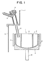
- FIG. 1 is a schematic cross-sectional view showing an example of an apparatus used in a method of manufacturing a silicon monocrystal according to the present invention;
- FIG. 2 is a graph illustrating the relationship between the weight W of crystallized silicon and a ratio of resistivity Cs(0)/Cs(W) of the silicon monocrystal to be pulled obtained when the silicon monocrystal is pulled without addition of dopant after commencement of pulling of the silicon monocrystal, with regard to the respective cases where the dopant concentration ratio obtained at the time of commencement of the pulling of the silicon monocrystal, or Coutl(0)/Cinl(0), is 0, 0.75, 2.0, and 3.0;
- FIG. 3 is a graph illustrating variations in Cs(0)/Cs(W) as a result of repetitive addition of a dopant to the silicon melt stored in the outer crucible according to the present invention, provided that the dopant concentration ratio at the time of commencement of the pulling of the silicon monocrystal is 2.0;
- FIG. 4 is a graph illustrating the relationship between Coutl(0)/Cinl(0) and the weight W of silicon which is crystallized until Cs(0)/Cs(W) returns to one; i.e., an initial value at the time of commencement of the pulling of the silicon monocrystal; as well as the relationship between Coutl(0)/Cinl(0) and W at a point of inflection in a Cs(0)/Cs(W) curve;
- FIG. 5 is a graph illustrating the relationship between Coutl(0)/Cinl(0) and the reciprocal of the ratio of resistivity of the silicon monocrystal to be pulled at a point of inflection of the Cs(0)/Cs(W) curve; i.e., Cs(W)/Cs(0);
- FIG. 6 is a graph illustrating the result of measurement of the ratio of resistivity of the silicon monocrystal according to an example of the present invention;
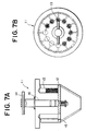
- FIG. 7A is a cross-sectional view of a dopant feeding apparatus of the present invention; and
- FIG. 7B is a plan view of the dopant feeding apparatus of the present invention.
- An embodiment of the present invention will now be described with reference to the drawings.
- In FIG. 1,
reference numeral 1 denotes a double quartz-crucible, 2 denotes an outer crucible, and 3 denotes an inner crucible. The double quartz-crucible 1 is supported by agraphite crucible 4 and is housed in achamber 5. Theouter crucible 2 and theinner crucible 3 communicate with each other through pores (not shown) formed in aninterior wall 7. Arotary shaft 8 is attached to thegraphite crucible 4, whereby the double quartz-crucible 1 and thegraphite crucible 4 can rotate and are vertically movable. When a silicon monocrystal is manufactured, the silicon melt stored in the double quartz-crucible 1 is heated by aheater 21, or silicon material and dopant supplied to the double quartz-crucible 1 are heated by theheater 21 so as to become melted. - The apparatus is equipped with a
feed pipe 10 for introducing granular silicon material into theouter crucible 2. The granular silicon material is supplied to thefeed pipe 10 from afeeder 6. Thefeeder 6 is capable of continuously or intermittently supplying the granular silicon material to thefeed pipe 10 in a fixed or variable amount. - Further, the present apparatus is equipped with a dopant feeding apparatus 9 capable of feeding a predetermined amount of dopant to silicon melt a plurality of times at desired points of time.
- In a CCZ method of manufacturing a silicon monocrystal according to the present invention, before pulling of the silicon monocrystal is commenced, the dopant is charged to the silicon melt stored in the double crucible such that the dopant concentration ratio is greater than an effective segregation coefficient; namely,

- While the silicon material is supplied to the silicon melt stored in the outer crucible via the feed pipe so as to maintain a constant amount of silicon melt in the double quartz-crucible, the pulling of the silicon monocrystal is continued. As a result of charging of the silicon material to the silicon melt stored in the outer crucible, the dopant concentration of the silicon melt stored in the outer crucible decreases. Eventually, the dopant concentration becomes equal to the effective segregation coefficient; namely,

- Further, while the granular silicon material is supplied to the silicon melt stored in the outer crucible via the feed pipe so as to maintain a constant amount of silicon melt in the double quartz-crucible, the pulling of the silicon monocrystal is continued. As a result of this, the dopant concentration of the silicon melt stored in the outer crucible decreases further. Eventually, the dopant concentration ratio becomes smaller than the effective segregation coefficient; namely,

- When the state (iii) has developed, the dopant is charged to the silicon melt stored in the outer crucible using the dopant feeding apparatus so as to cause the dopant concentration ratio to again become

- Subsequently, if the dopant concentration ratio becomes smaller than the effective segregation coefficient, charging of the dopant to the silicon melt stored in the outer crucible is repeated, whereby Cinl(W) can be controlled within a certain range. As a result, the ratio of resistivity of the silicon monocrystal; namely, Cs(0)/Cs(W), can be controlled within a constant range.
- The method of manufacturing a silicon monocrystal will be described in more detail with reference to FIGS. 2 through 5.
- The dopant has been previously charged to the silicon melt before a silicon material is pulled. After the pulling of the silicon monocrystal has been commenced, the dopant is not charged to the silicon melt. In this state, while the granular silicon material is supplied via the feed pipe to the silicon melt stored in the outer crucible so as to maintain a constant amount of silicon melt in the double quartz-crucible, the silicon monocrystal is pulled. At this time, the relationship between the weight W of crystallized silicon and the dopant concentration Cinl(W) of the silicon melt of the inner crucible obtained at the weight W is expressed by Equation (1):

- FIG. 2 illustrates the relationship between the weight W of crystallized silicon and the ratio of resistivity Cs(0)/Cs(W) of the silicon monocrystal to be pulled obtained when the silicon monocrystal is pulled without addition of dopant after commencement of pulling of the silicon monocrystal, with regard to the respective cases where the dopant concentration ratio obtained at the time of commencement of the pulling of the silicon monocrystal, or Coutl(0)/Cinl(0), is 0, 0.75 (which is the keff of boron), 2.0, and 3.0. Using Equation (2), Cs(W) is calculated from Cinl(W) obtained by Equation (1).

- As illustrated in FIG. 2, where Coutl(0)/Cinl(0) is larger than keff, or where Coutl(0)/Cinl(0) is 2.0 or 3.0, the ratio of resistivity Cs(0)/Cs(W) temporarily decreases so as to be smaller than one which is the value at the time of commencement of silicon monocrystal to be pulled. Then, the ratio of resistivity returns to one and further increases so as to be larger than one.
- FIG. 3 is a graph illustrating variations in Cs(0)/Cs(W) as a result of repetitive addition of the dopant to the silicon melt stored in the outer crucible according to the present invention, provided that the dopant concentration ratio obtained at the time of commencement of the pulling of the silicon monocrystal is 2.0.
- As illustrated in FIG. 3, it is understood that the ratio of resistivity Cs(0)/Cs(W) is controlled within a constant range by charging the dopant to the silicon melt of the outer crucible.
- In the present invention, before commencement of or during the course of pulling of a silicon monocrystal, the dopant concentration ratio - i.e., Coutl(W1)/Cinl(W1) or Coutl(W1')/Cinl(W1') - is increased so as to become larger than the effective segregation coefficient (keff). If this ratio is increased, the number of times that the dopant is charged per weight of crystallized silicon, will decrease. However, as illustrated in FIG. 4, the weight (W) of silicon which is crystallized until Cs(0)/Cs(W) returns to one; i.e., a value before commencement of pulling of the silicon monocrystal, increases. As can be seen from FIG. 5, as the weight of the crystallized silicon increases, the range of resistivity ratio of the silicon monocrystal to be pulled becomes larger. Accordingly, it is not desirable to excessively increase Coutl(W1)/Cinl(W1) and Coutl(W1')/Cinl(W1').
- FIG. 4 is a graph illustrating the relationship between Coutl(0)/Cinl(0) and the weight W of silicon which is crystallized until Cs(0)/Cs(W) returns to one - i.e., an initial value at the time of commencement of the pulling of the silicon monocrystal; as well as the relationship between Coutl(0)/Cinl(0) and W at a point of inflection in a Cs(0)/Cs(W) curve.
- FIG. 5 is a graph illustrating the relationship between Coutl(0)/Cinl(0) and the reciprocal of the ratio of resistivity of the silicon monocrystal to be pulled at a point of inflection of the Cs(0)/Cs(W) curve; i.e., Cs(W)/Cs(0).
- According to the silicon monocrystal manufacturing method of the present invention, dopant is charged to the outer crucible several times during the course of pulling of the silicon monocrystal. The charging of dopant to the silicon melt does not require any special dopant feeding equipment. A dopant feeding apparatus of any type may be used so long as it has a plurality of dopant storage sections and is capable of charging a predetermined amount of dopant to silicon melt several times at desired points in time. For example, a dopant feeding apparatus 11 as provided in FIGS. 7A and 7B is used.
- The dopant feeding apparatus 11 is provided with a plurality of
dopant feed pipes 13 which serve as dopant storage sections. More specifically, in the dopant feeding apparatus 11 shown in FIGS. 7A and 7B, the twelvefeed pipes 13 are provided at 30° intervals around arotary shaft 16. The lower ends of thedopant feed pipes 13 are open and in contact with adisk member 12, whereby the dopant stored in the dopant feed pipes is prevented from being discharged. Thedisk member 12 is rotatable about therotary shaft 16. By rotation of ahandle 14 mounted on the uppermost end of therotary shaft 16, thedisk member 12 can be rotated via therotary shaft 16. Oneaperture 15 is formed in thedisk member 12. When theaperture 15 is brought in line with the open end of eachdopant feed pipe 13 by rotating thedisk member 12 using thehandle 14, the dopant stored in thefeed pipe 13 is added to the silicon melt through theaperture 15. Where the dopant feeding apparatus shown in FIGS. 7A and 7B is used, the amount of dopant required by one charging operation is previously stored in each of thefeed pipes 13. Therefore, by rotating thedisk member 12 by an angle of 30° using thehandle 14, a predetermined amount of dopant can be supplied to the silicon melt stored in the outer crucible several times at desired points in time. - The
dopant feed pipes 13 may be arranged linearly. Further, although one disk member is used in the dopant feeding apparatus shown in FIGS. 7A and 7B, a member of any shape may be used so long as it is capable of preventing the dopant stored in the dopant feed pipes from being discharged. Further, the number of members is not limited to one. Further, the dopant feed pipes may be movably arranged so long as theaperture 15 formed in thedisk member 12 can be brought in alignment with the open ends of the dopant feed pipes at a desired time. - An example of the present invention will now be described.
- Through use of a double crucible consisting of an outer crucible having a diameter of 18 inches and an inner crucible having a diameter of 14 inches, a silicon monocrystal having a diameter of 6 inches was manufactured using a CCZ method.
- The double crucible was filled with silicon melt, and dopant was charged to the outer and inner crucibles before commencement of pulling of a silicon monocrystal such that the dopant concentration of the silicon melt stored in the outer crucible became twice that of the silicon melt stored in the inner crucible. Subsequently, the pulling of a silicon monocrystal was commenced. At this time, the amount of the silicon melt stored in the double crucible was maintained constant by supplying granular silicon material to the outer crucible through the feed pipe.
- When the dopant concentration ratio became smaller than the effective segregation coefficient, and the dopant concentration of the silicon melt of the inner crucible became equal to the dopant concentration of the silicon melt of the inner crucible before the pulling of the silicon monocrystal was started; more specifically, when the weight of the crystallized silicon reached 5 kg, 23 kg, or 34 kg (or when the length of the body portion of the silicon monocrystal to be pulled reached 10 cm, 50 cm, or 75 cm), the dopant concentration of the silicon melt of the outer crucible was controlled so as to become equal to the dopant concentration of the silicon melt of the outer crucible before commencement of pulling of the silicon monocrystal, by charging the dopant to the silicon melt of the outer crucible using the dopant feeding apparatus.
- FIG. 6 illustrates results of measurement of the ratio of resistivity [that is, Cs(0)/Cs(W)] of the silicon monocrystal that was pulled in the test.
- As is seen from FIG. 6, the reciprocal of the ratio of resistivity of the silicon monocrystal was able to be controlled so as to become less than 1.3.
Claims (6)
- A method of manufacturing a silicon monocrystal according to the continuously charged Czochralski method in which the silicon monocrystal is pulled while silicon material is charged to silicon melt stored in a crucible, characterized in that said crucible is a double crucible composed of an outer crucible and an inner crucible which communicate with each other through pores, and said method comprises the steps of:(a) charging a dopant to the silicon melt stored in the double crucible before commencing pulling of a silicon monocrystal such that the ratio of the dopant concentration of the silicon melt stored in the outer crucible to the dopant concentration of the silicon melt stored in the inner crucible becomes greater than an effective segregation coefficient of the dopant;(b) pulling the silicon monocrystal while charging silicon material to the silicon melt within the outer crucible, during which the dopant concentration ratio becomes equal to the effective segregation coefficient and then becomes smaller than the effective segregation coefficient;(c) recharging the dopant to the silicon melt stored in the outer crucible when the dopant concentration ratio becomes smaller than the effective segregation coefficient such that the ratio of the dopant concentration of the silicon melt stored in the outer crucible to the dopant concentration of the silicon melt stored in the inner crucible becomes greater than the effective segregation coefficient; and(d) repeating the recharging step (c).
- A method of manufacturing a silicon monocrystal according to Claim 1, characterized in that when the dopant concentration of the silicon melt stored in the inner crucible becomes equal to its initial value before commencement of pulling of the silicon monocrystal, the dopant is charged to the silicon melt of the outer crucible.
- A method of manufacturing a silicon monocrystal according to Claim 1, characterized in that when the dopant concentration of the silicon melt stored in the inner crucible becomes equal to its initial value before commencement of pulling of the silicon monocrystal, the dopant concentration of the silicon melt stored in the outer crucible is made equal to its initial value before commencement of pulling of the silicon monocrystal by charging the dopant to the silicon melt of the outer crucible.
- A dopant feeding apparatus characterized by comprising a plurality of dopant storage sections and being capable of charging dopant to silicon melt a plurality of times.
- A dopant feeding apparatus characterized by comprising:a plurality of dopant feed pipes each of which has an open end and is adapted to store dopant; andat least one plate member disposed in contact with the open end and having an aperture for discharging the dopant stored in each dopant feed pipe through the open end thereof, said plate member being moved such that the aperture of said plate member faces the open end of said dopant feed pipe when the dopant is to be discharged.
- A dopant feeding apparatus according to Claim 5, characterized in that said a plurality of dopant feed pipes are arranged in a circle, said plate member is disposed in a rotatable manner, and when the dopant is to be discharged, said plate member is rotated such that the aperture of said plate member faces the open end of said dopant feed pipe.
Applications Claiming Priority (2)
| Application Number | Priority Date | Filing Date | Title |
|---|---|---|---|
| JP09770096A JP3484870B2 (en) | 1996-03-27 | 1996-03-27 | Method for producing silicon single crystal by continuous charge method and dopant supply apparatus |
| JP97700/96 | 1996-03-27 |
Publications (1)
| Publication Number | Publication Date |
|---|---|
| EP0798403A1 true EP0798403A1 (en) | 1997-10-01 |
Family
ID=14199212
Family Applications (1)
| Application Number | Title | Priority Date | Filing Date |
|---|---|---|---|
| EP97302063A Withdrawn EP0798403A1 (en) | 1996-03-27 | 1997-03-26 | Continuously charged czochralski method of manufacturing silicon monocrystal, and dopant feeding apparatus |
Country Status (3)
| Country | Link |
|---|---|
| US (1) | US5900055A (en) |
| EP (1) | EP0798403A1 (en) |
| JP (1) | JP3484870B2 (en) |
Cited By (5)
| Publication number | Priority date | Publication date | Assignee | Title |
|---|---|---|---|---|
| WO2007032799A1 (en) * | 2005-09-12 | 2007-03-22 | Rexor Corporation | Method and apparatus to produce single crystal ingot of uniform axial resistivity |
| EP2697412A4 (en) * | 2011-04-14 | 2014-09-03 | Gt Advanced Cz Llc | SILICON INGOT WITH MULTIPLE UNIFORM DOPANTS AND METHOD AND APPARATUS FOR PRODUCING THE SAME |
| US9051659B2 (en) | 2010-09-03 | 2015-06-09 | Gtat Ip Holding | Silicon single crystal doped with gallium, indium, or aluminum |
| CN109850905A (en) * | 2019-04-16 | 2019-06-07 | 大连理工大学 | Method and device for improving impurity removal amount of volatile impurities in electron beam melting process |
| CN112210822A (en) * | 2020-09-10 | 2021-01-12 | 徐州鑫晶半导体科技有限公司 | Crucible assembly for single crystal furnace and single crystal furnace |
Families Citing this family (21)
| Publication number | Priority date | Publication date | Assignee | Title |
|---|---|---|---|---|
| DE19813453A1 (en) * | 1998-03-26 | 1999-09-30 | Leybold Systems Gmbh | Crystal drawing system |
| US6179914B1 (en) * | 1999-02-02 | 2001-01-30 | Seh America, Inc. | Dopant delivery system and method |
| US6491752B1 (en) * | 1999-07-16 | 2002-12-10 | Sumco Oregon Corporation | Enhanced n-type silicon material for epitaxial wafer substrate and method of making same |
| JP2001214187A (en) * | 2000-02-04 | 2001-08-07 | Nippon Mitsubishi Oil Corp | Hydraulic fluid composition |
| DE10007179B4 (en) * | 2000-02-17 | 2004-08-19 | Siltronic Ag | Method and device for doping a melt with a dopant |
| US7132091B2 (en) * | 2001-09-28 | 2006-11-07 | Memc Electronic Materials, Inc. | Single crystal silicon ingot having a high arsenic concentration |
| WO2004097079A2 (en) * | 2003-04-24 | 2004-11-11 | Bryan Fickett | Source material feeder apparatus for industrial crystal growth systems |
| US7001456B2 (en) * | 2003-05-16 | 2006-02-21 | Sumitomo Mitsubishi Silicon Corporation | Apparatus and method for supplying Crystalline materials in czochralski method |
| US7635414B2 (en) * | 2003-11-03 | 2009-12-22 | Solaicx, Inc. | System for continuous growing of monocrystalline silicon |
| EP1577954A1 (en) * | 2004-03-09 | 2005-09-21 | RWE SCHOTT Solar GmbH | Method for transporting solid particles |
| WO2007120871A2 (en) * | 2006-04-13 | 2007-10-25 | Cabot Corporation | Production of silicon through a closed-loop process |
| JP5313534B2 (en) * | 2008-03-28 | 2013-10-09 | Sumco Techxiv株式会社 | Silicon single crystal pulling apparatus and silicon single crystal manufacturing method |
| US7922817B2 (en) * | 2008-04-24 | 2011-04-12 | Memc Electronic Materials, Inc. | Method and device for feeding arsenic dopant into a silicon crystal growing apparatus |
| JP5397736B2 (en) * | 2008-09-25 | 2014-01-22 | 日本電気硝子株式会社 | Float glass manufacturing apparatus and float glass manufacturing method |
| JP5222162B2 (en) * | 2009-01-16 | 2013-06-26 | Sumco Techxiv株式会社 | Method for producing silicon single crystal |
| US8535439B2 (en) | 2009-01-14 | 2013-09-17 | Sumco Techxiv Corporation | Manufacturing method for silicon single crystal |
| MY169752A (en) | 2011-05-06 | 2019-05-15 | Gt Advanced Cz Llc | Growth of a uniformly doped silicon ingot by doping only the initial charge |
| KR101494532B1 (en) | 2013-06-27 | 2015-02-17 | 웅진에너지 주식회사 | The method of manufacturing master dopant using remain silicon melt |
| EP3700860A4 (en) | 2017-10-27 | 2021-08-11 | Northern Silicon Inc. | HIGH PURITY SILICON PRODUCTION SYSTEM AND PROCESS |
| CN111962140A (en) * | 2020-08-28 | 2020-11-20 | 晶科绿能(上海)管理有限公司 | Continuous crystal pulling apparatus and method for continuously pulling crystal rod |
| US20260015763A1 (en) * | 2024-07-10 | 2026-01-15 | GlobalWafer Co., Ltd. | Systems and methods for adding dopant to an ingot puller apparatus |
Citations (6)
| Publication number | Priority date | Publication date | Assignee | Title |
|---|---|---|---|---|
| FR1196081A (en) * | 1958-05-10 | 1959-11-20 | Telecommunications Sa | Advanced training in semiconductor crystal printing machines |
| FR1204436A (en) * | 1958-03-29 | 1960-01-26 | Automatic device for the addition of impurities during the pulling of transistrons with junctions | |
| DE2152801A1 (en) * | 1970-11-09 | 1972-05-10 | Little Inc A | Method and furnace for pulling crystals of uniform composition according to the Czochralski method |
| EP0330189A2 (en) * | 1988-02-25 | 1989-08-30 | Kabushiki Kaisha Toshiba | Semiconductor crystal pulling method |
| EP0350305A2 (en) * | 1988-07-07 | 1990-01-10 | Nkk Corporation | Method and apparatus for manufacturing silicon single crystals |
| EP0388503A1 (en) * | 1989-02-03 | 1990-09-26 | Mitsubishi Materials Corporation | Method for pulling single crystals |
Family Cites Families (2)
| Publication number | Priority date | Publication date | Assignee | Title |
|---|---|---|---|---|
| US2892739A (en) * | 1954-10-01 | 1959-06-30 | Honeywell Regulator Co | Crystal growing procedure |
| JPH01192789A (en) * | 1988-01-27 | 1989-08-02 | Toshiba Corp | Crystal-pulling up device and pulling up method |
-
1996
- 1996-03-27 JP JP09770096A patent/JP3484870B2/en not_active Expired - Fee Related
-
1997
- 1997-03-25 US US08/829,894 patent/US5900055A/en not_active Expired - Fee Related
- 1997-03-26 EP EP97302063A patent/EP0798403A1/en not_active Withdrawn
Patent Citations (6)
| Publication number | Priority date | Publication date | Assignee | Title |
|---|---|---|---|---|
| FR1204436A (en) * | 1958-03-29 | 1960-01-26 | Automatic device for the addition of impurities during the pulling of transistrons with junctions | |
| FR1196081A (en) * | 1958-05-10 | 1959-11-20 | Telecommunications Sa | Advanced training in semiconductor crystal printing machines |
| DE2152801A1 (en) * | 1970-11-09 | 1972-05-10 | Little Inc A | Method and furnace for pulling crystals of uniform composition according to the Czochralski method |
| EP0330189A2 (en) * | 1988-02-25 | 1989-08-30 | Kabushiki Kaisha Toshiba | Semiconductor crystal pulling method |
| EP0350305A2 (en) * | 1988-07-07 | 1990-01-10 | Nkk Corporation | Method and apparatus for manufacturing silicon single crystals |
| EP0388503A1 (en) * | 1989-02-03 | 1990-09-26 | Mitsubishi Materials Corporation | Method for pulling single crystals |
Cited By (6)
| Publication number | Priority date | Publication date | Assignee | Title |
|---|---|---|---|---|
| WO2007032799A1 (en) * | 2005-09-12 | 2007-03-22 | Rexor Corporation | Method and apparatus to produce single crystal ingot of uniform axial resistivity |
| US9051659B2 (en) | 2010-09-03 | 2015-06-09 | Gtat Ip Holding | Silicon single crystal doped with gallium, indium, or aluminum |
| EP2697412A4 (en) * | 2011-04-14 | 2014-09-03 | Gt Advanced Cz Llc | SILICON INGOT WITH MULTIPLE UNIFORM DOPANTS AND METHOD AND APPARATUS FOR PRODUCING THE SAME |
| US10202705B2 (en) | 2011-04-14 | 2019-02-12 | Gtat Ip Holding Llc | Silicon ingot having uniform multiple dopants and method and apparatus for producing same |
| CN109850905A (en) * | 2019-04-16 | 2019-06-07 | 大连理工大学 | Method and device for improving impurity removal amount of volatile impurities in electron beam melting process |
| CN112210822A (en) * | 2020-09-10 | 2021-01-12 | 徐州鑫晶半导体科技有限公司 | Crucible assembly for single crystal furnace and single crystal furnace |
Also Published As
| Publication number | Publication date |
|---|---|
| JP3484870B2 (en) | 2004-01-06 |
| US5900055A (en) | 1999-05-04 |
| JPH09263492A (en) | 1997-10-07 |
Similar Documents
| Publication | Publication Date | Title |
|---|---|---|
| US5900055A (en) | Method of manufacturing silicon monocrystal by continuously charged Czochralski method | |
| Abrosimov et al. | Single crystal growth of Si1− xGex by the Czochralski technique | |
| US3359077A (en) | Method of growing a crystal | |
| CN103249875B (en) | Gallium, indium or aluminum doped monocrystalline silicon | |
| DE69205253T2 (en) | Device for feeding granulated bulk material for a semiconductor single crystal pulling apparatus. | |
| US4249988A (en) | Growing crystals from a melt by controlling additions of material thereto | |
| CN1020767C (en) | Method and equipment for manufacturing silicon single crystal | |
| EP4271862B1 (en) | Use of buffer members during growth of single crystal silicon ingots | |
| EP0388503B1 (en) | Method for pulling single crystals | |
| EP0098471A2 (en) | Method of growing silicon crystals by the Czochralski method | |
| EP0055619B1 (en) | Method for regulating concentration and distribution of oxygen in czochralski grown silicon | |
| Leverton | Floating crucible technique for growing uniformly doped crystals | |
| US20070056504A1 (en) | Method and apparatus to produce single crystal ingot of uniform axial resistivity | |
| KR20070038578A (en) | Intermittent dosing technology to increase the melt rate of polycrystalline silicon | |
| US6080238A (en) | Single crystal pulling method | |
| US6179914B1 (en) | Dopant delivery system and method | |
| EP0330189B1 (en) | Semiconductor crystal pulling method | |
| JP3598642B2 (en) | Method for producing silicon single crystal by continuous charge method | |
| US4496424A (en) | Method for manufacture of III-V compound semiconducting single crystal | |
| JPH11312683A (en) | Manufacturing method of semiconductor single crystal silicon | |
| JPH034517B2 (en) | ||
| EP0553677B1 (en) | Monocrystal growing method | |
| CN116783333B (en) | Method for growing single crystal silicon ingot by continuous Czochralski method | |
| JP2721242B2 (en) | Silicon single crystal pulling method | |
| US5681758A (en) | Method for fabricating semiconductor single crystal |
Legal Events
| Date | Code | Title | Description |
|---|---|---|---|
| PUAI | Public reference made under article 153(3) epc to a published international application that has entered the european phase |
Free format text: ORIGINAL CODE: 0009012 |
|
| AK | Designated contracting states |
Kind code of ref document: A1 Designated state(s): DE FR GB |
|
| 17P | Request for examination filed |
Effective date: 19970915 |
|
| STAA | Information on the status of an ep patent application or granted ep patent |
Free format text: STATUS: THE APPLICATION IS DEEMED TO BE WITHDRAWN |
|
| 18D | Application deemed to be withdrawn |
Effective date: 20001001 |