EP0797291A2 - Procédé pour fournir une impédance prédéterminée au circuit de sortie d'un onduleur - Google Patents
Procédé pour fournir une impédance prédéterminée au circuit de sortie d'un onduleur Download PDFInfo
- Publication number
- EP0797291A2 EP0797291A2 EP97103947A EP97103947A EP0797291A2 EP 0797291 A2 EP0797291 A2 EP 0797291A2 EP 97103947 A EP97103947 A EP 97103947A EP 97103947 A EP97103947 A EP 97103947A EP 0797291 A2 EP0797291 A2 EP 0797291A2
- Authority
- EP
- European Patent Office
- Prior art keywords
- output
- transformation
- offset
- inverter
- voltages
- Prior art date
- Legal status (The legal status is an assumption and is not a legal conclusion. Google has not performed a legal analysis and makes no representation as to the accuracy of the status listed.)
- Withdrawn
Links
- 238000000034 method Methods 0.000 title claims abstract description 31
- 239000003990 capacitor Substances 0.000 claims abstract description 12
- 230000009466 transformation Effects 0.000 claims description 44
- 230000010355 oscillation Effects 0.000 claims description 2
- 230000001131 transforming effect Effects 0.000 claims 4
- 230000001105 regulatory effect Effects 0.000 abstract description 4
- 239000013598 vector Substances 0.000 description 14
- 238000010586 diagram Methods 0.000 description 12
- 239000004020 conductor Substances 0.000 description 4
- 230000007935 neutral effect Effects 0.000 description 3
- XEEYBQQBJWHFJM-UHFFFAOYSA-N Iron Chemical compound [Fe] XEEYBQQBJWHFJM-UHFFFAOYSA-N 0.000 description 2
- 230000033228 biological regulation Effects 0.000 description 2
- 230000001629 suppression Effects 0.000 description 2
- 230000001419 dependent effect Effects 0.000 description 1
- 229910052742 iron Inorganic materials 0.000 description 1
- 238000004804 winding Methods 0.000 description 1
Images


Classifications
-
- H—ELECTRICITY
- H02—GENERATION; CONVERSION OR DISTRIBUTION OF ELECTRIC POWER
- H02M—APPARATUS FOR CONVERSION BETWEEN AC AND AC, BETWEEN AC AND DC, OR BETWEEN DC AND DC, AND FOR USE WITH MAINS OR SIMILAR POWER SUPPLY SYSTEMS; CONVERSION OF DC OR AC INPUT POWER INTO SURGE OUTPUT POWER; CONTROL OR REGULATION THEREOF
- H02M7/00—Conversion of AC power input into DC power output; Conversion of DC power input into AC power output
- H02M7/42—Conversion of DC power input into AC power output without possibility of reversal
- H02M7/44—Conversion of DC power input into AC power output without possibility of reversal by static converters
- H02M7/48—Conversion of DC power input into AC power output without possibility of reversal by static converters using discharge tubes with control electrode or semiconductor devices with control electrode
- H02M7/53—Conversion of DC power input into AC power output without possibility of reversal by static converters using discharge tubes with control electrode or semiconductor devices with control electrode using devices of a triode or transistor type requiring continuous application of a control signal
- H02M7/537—Conversion of DC power input into AC power output without possibility of reversal by static converters using discharge tubes with control electrode or semiconductor devices with control electrode using devices of a triode or transistor type requiring continuous application of a control signal using semiconductor devices only, e.g. single switched pulse inverters
- H02M7/5387—Conversion of DC power input into AC power output without possibility of reversal by static converters using discharge tubes with control electrode or semiconductor devices with control electrode using devices of a triode or transistor type requiring continuous application of a control signal using semiconductor devices only, e.g. single switched pulse inverters in a bridge configuration
- H02M7/53871—Conversion of DC power input into AC power output without possibility of reversal by static converters using discharge tubes with control electrode or semiconductor devices with control electrode using devices of a triode or transistor type requiring continuous application of a control signal using semiconductor devices only, e.g. single switched pulse inverters in a bridge configuration with automatic control of output voltage or current
- H02M7/53875—Conversion of DC power input into AC power output without possibility of reversal by static converters using discharge tubes with control electrode or semiconductor devices with control electrode using devices of a triode or transistor type requiring continuous application of a control signal using semiconductor devices only, e.g. single switched pulse inverters in a bridge configuration with automatic control of output voltage or current with analogue control of three-phase output
Definitions
- the invention relates to a method for specifying a predetermined output impedance of an output circuit of an inverter, the output circuit having a sine filter, a transformer and an output capacitor, the transformer being connected in a triangle on the primary side and in a star on the secondary side, and to a device for carrying it out Procedure.
- Such an arrangement - inverters with a downstream output circuit - occurs, for example, in the case of uninterruptible power supplies (UPS), the controlled system being the output circuit of the UPS and the actuator of the inverter of the UPS.
- UPS uninterruptible power supplies
- a three-phase voltage system is available at the output of the output circuit, which is, for example, the voltage system of the safe rail of a UPS.
- This voltage system is generated by the inverter, in particular a pulse inverter.
- a sine filter consisting of LC resonant circuits matched to the clock frequency, is provided.
- the transformer is provided on the one hand for decoupling the three-phase voltage system on the output side and the output system of the inverter, and on the other hand for generating three line voltages with a neutral conductor.
- the output circuit of the inverter has an output capacitor for reactive current compensation, this output capacitor having one capacitor per phase, which are connected in a triangle.
- the first peculiarity of the controlled system is the fact that the transformer is connected on the primary side in a triangle and on the secondary side in a star. This gives route two Control inputs (primary-side chained voltages), but three outputs (three secondary-side line voltages). Obviously there is a portion in the output voltages that cannot be influenced by the primary voltages of the transformer. This non-controllable part is the zero system, that is, an in-phase part in all three output voltages. The size of this portion is essentially determined by the electrical properties (losses, control) of the transformer. The smaller the losses and the control, the smaller the zero component in the three output voltages. Since it cannot be influenced by the control inputs, the zero component must be removed from the system equations when designing the controller.
- the output capacitor together with the leakage inductance of the transformer, forms a weakly damped series resonant circuit.
- the output circuit contains a number of resonance frequencies, one of which is usually in the range between 200 Hz and 500 Hz.
- the output impedance of this arrangement (for example a UPS) is particularly high at the resonance frequency and causes an intolerable distortion of the output voltage, especially where typical UPS loads generate higher harmonics in the load current.
- the main disturbance variable is the load current. Combating its influence is difficult because it does not arise independently, but is formed from the output voltage via the load.
- the greater the current and thus the disturbance variable In the case of nonlinear loads, it has a high proportion of higher harmonics, which become larger the more their influence on the output voltage is combated.
- the interference frequency response of the line is the transfer function of the interference variable to the output variable, i.e. here the output impedance. The smaller the output impedance, the more independent the output voltage is from the load and the less its distortion (the distortion factor) with a non-linear load.
- the invention is based on the object of specifying a method and a device with which a predetermined output impedance can be predetermined.
- the in-phase component in the three output voltages must be calculated out.
- An aid to this, which divides a three-phase system into two linearly independent quantities and the zero system, is a transformation, which is also referred to in the literature as the Clarke transformation. If, for example, the three phases of the three-phase system are symmetrical (three sine functions offset by 120 °), then by using the transformation two sine functions offset by 90 ° are obtained and as zero system identical zero.
- the two new sizes are commonly referred to as ⁇ , ⁇ sizes.
- the ⁇ component of the output voltage of the output circuit is equal to the phase R phase voltage against the neutral conductor and the ⁇ component equal to the chained voltage between phases S and T divided by ⁇ 3.
- the ⁇ component and the ⁇ component form a complex vector, which is referred to in the literature as a park vector. In a symmetrical three-phase system, its magnitude is constant and it rotates at the frequency of the three-phase system around the zero point of the complex plane.
- correction variables for the reference variables are generated by means of two identical single-variable controllers depending on the control variable.
- the inverter output current is required to control some operating cases with a UPS, such as short circuit and parallel operation.
- the determined ⁇ -, ⁇ -command correction variables are added to the command variable component by component and then the ⁇ -, ⁇ -sum components are transformed back into a three-phase manipulated variable system with which the inverter is controlled.
- the weakly damped resonant line poles are shifted into predetermined complex poles as a function of a predetermined impedance. That is, the interference frequency response of the link is set to a predetermined value, whereby good interference suppression is achieved.
- the smaller the output impedance the more independent the output voltage is from the Load and the smaller their distortion (distortion factor) becomes with non-linear load.
- the output impedance is advantageously regulated to a constant value up to a certain limit frequency.
- a guidance regulation is added to the method already explained.
- This master control ensures that the controlled variable output voltage of the output circuit tracks the reference variable target voltage. This means that control deviations occurring in the output voltage of the output circuit are controlled to zero.
- the master controller Since the three-phase nominal voltage system and the three-phase output voltage system are each already transformed into a complex vector with the Cartesian coordinates ⁇ and ⁇ components, it makes sense to use a complex integrator as the master controller.
- the complex integrator can only be used for the constant values, so that the sinusoidal reference variables must be transformed into constant values. If setpoints and actual values are viewed as a clockwise rotating vector that is transformed into equal quantities, the master controller is a single, complex integrator. However, this alone has inadequate unbalanced load behavior, so that an additional transformation into equal quantities is introduced, in which the setpoint and actual values are each interpreted as left-rotating vectors. A master controller must also be provided for the left-circulating setpoint.
- the advantageous method is therefore based on the knowledge that the guidance control is carried out in a coordinate system rotating at the mains frequency instead of in a stationary coordinate system.
- This transformation now gives four direct variables for the master control for the command variable and the controlled variable, each of which is fed to a constant variable master control, consisting of a comparator, I controller and addition point.
- the four output direct variables of this direct variable control are then transformed back into a rotating complex vector which is used in the method according to claim 1.
- the inverter 2 is provided with an intermediate circuit capacitor or a battery 8, a control set 10 being provided for generating control signals for the inverter 2, at the actuating inputs of which a control variable y 1 , y 2 , y 3 of a three-phase control variable system are present.
- These manipulated variables y 1 , y 2 , y 3 are generated by the device 6.
- the following variables are required when using the method according to the invention: the output voltages u A1 , u A2 , u A3 of the output circuit 4, the inverter output currents i f1 , i f2 , i f3 and the command variables u W1 , u W2 , u W3 , which are provided by a three-phase setpoint generator 12. If the method according to the invention is not used, the command variables u W1 , u W2 , u W3 are output as manipulated variables y 1 , y 2 , y 3 .
- a three-phase 50 Hz voltage system is provided as the reference variable system.
- the controlled system is then the output circuit of the UPS.
- the output circuit 4 is an electrical three-phase system which contains a sine filter 14, a three-leg transformer 16 and an output capacitor 18.
- the actuator is the inverter 2 of the UPS. To simplify matters, it is modeled as an amplifier, which receives gain one if the path constants are appropriately normalized.
- the first peculiarity of the controlled system is the fact that the transformer 16 is connected on the primary side in a triangle and on the secondary side in a star.
- This non-controllable component is the so-called zero system, ie a three-phase component in all three output voltages u A1 , u A2 and u A3 .
- the size of this component is essentially determined by the electrical properties (losses, scatter) of the transformer 16. The smaller the losses and the scatter, the smaller the zero component in the three output voltages u A1 , u A2 , u A3 . Since this zero component cannot be influenced by the control inputs, it must be calculated from the system equations when designing a controller.
- transformer 16 Another property of the controlled system results from the fact that the transformer 16 cannot transmit direct voltages. If voltages containing DC components are applied to the line entrance, they are no longer available at the line exit. However, they are noticeable in another way: the transformer 16 saturates.
- the resonance frequency is approximately 200 Hz to 500 Hz. This resonance greatly distorts the output voltage when the load is non-linear.
- the in-phase component in the three output voltages u A1 , u A2 , u A3 must be calculated out.
- An aid to this, which divides a three-phase system into two linearly independent quantities and the zero system, is a three-two transformation, also known in the literature as Label Clarke transformation. If, for example, the three phases are symmetrical (three sine functions offset by 120 °), using this known Clarke transformation one obtains two sine oscillations offset by 90 ° and as zero system identically zero. The two new sizes are then called ⁇ , ⁇ sizes.
- the ⁇ component of the output voltage is equal to the line voltage u A1 against the neutral conductor and the ⁇ component is equal to the wrong voltage between u A2 and u A3 divided by ⁇ 3.
- These two components form a complex vector on the complex level, which is referred to in the literature as a park vector.
- a park vector In a symmetrical three-phase system, its magnitude is constant and it rotates at the frequency of the three-phase system around the zero point of the complex plane.
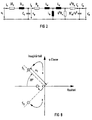
- the ⁇ , ⁇ components have identical single-phase equivalent circuit diagrams, one of which is shown in FIG. 2. These single-phase equivalent circuit diagrams are hardly interconnected, i.e. the ⁇ component of the output voltage is identical to zero if the path is only excited with the ⁇ component of the input voltage and vice versa.
- the curve of the output impedance marked with a is obtained, i.e. the transfer function from the load current to the output voltage ( Figure 3).
- the curve marked b shows the reference frequency response, i.e. the transfer function from the desired output voltage profile to the actual profile of the inverter 2 with a downstream output circuit 4.
- the profile of the output impedance is identified by a ', and the reference frequency response, indicated by b', of the inverter 2 shown the inventive method.
- FIG. 5 shows an equivalent circuit diagram of the device 6 for carrying out the method according to the invention.
- This equivalent circuit diagram is an advantageous embodiment of the device 6.
- This advantageous embodiment of the device 6 has a part 20 consisting of the transformation devices 22, 24 and 26, the two single-size controllers 28 and 30, the two addition points 32 and 34 and one Reverse transformation device 36, and a further part 38, consisting of the further transformation devices 40 and 42, the comparators 44, 46, 48 and 50, the controllers 52, 54, 56 and 58, the further addition points 60, 62, 64, 66 and one further reverse transformation device 68.
- the part 20 can also be operated without the further part 38.
- a predetermined output impedance of the output circuit 4 can be set by means of the part 20 of this device 6. With the further part 38 of this device 6, the leadership behavior is significantly improved.
- the command variables u W1 , u W2 , u W3 or the output voltages u A1 , u A2 , u A3 or the inverter output currents i f1 , i f2 , i f3 are converted into two 90s ° offset ⁇ , ⁇ components transformed.
- the ⁇ and ⁇ components of the output voltage and the ⁇ and ⁇ components of the inverter output current become component by component one size controller 28 and 30 each supplied.
- These size regulators 28 and 30, in particular state regulators generate an ⁇ and ⁇ component of a correction voltage u as a function of the ⁇ or ⁇ component of the transformed output voltage u A ⁇ , u A ⁇ with the aid of the transformed inverter output current i f ⁇ , i f ⁇ K ⁇ , u K ⁇ , which are added component by component to the transformed reference variable y ⁇ , y ⁇ by means of the addition points 32 and 34. If the further part 38 of the device 6 is not present, the ⁇ component u W ⁇ of the command variable u W is directly connected to the addition point 32 and the ⁇ component u W ⁇ is connected directly to the addition point 34.
- the identical Einierenregler 28 and 30 are designed so that the transformed reference variable u W ⁇ , u W ⁇ is changed in such a manner by means of the correction voltage u Ka, u K ⁇ that the lightly damped resonant route poles at a suitable location S1 and S2 of the complex plane ( Figure 8 ) are moved.
- These suitable points S1 and S2 are determined as a function of a desired output impedance of the output circuit 4 of the inverter 2.
- the course of the output impedance a 'obtained over the frequency is shown in FIG.
- a comparison with the course of the output impedance a of the controlled operation shows that the resonance increase is no longer present. This excessive resonance is responsible for the voltage distortion.
- a constant course of the output impedance is obtained up to the cutoff frequency.
- the further part 38 of the device 6 is provided.
- the rotating vector u W ⁇ , u w ⁇ becomes the reference variable u W and the rotating vector u A ⁇ , u A ⁇ the output variable u A in the complex plane into a space pointer u WDR , u WDL , u WQR , u WQL of the reference variable u W and a space pointer u ADR , u ADL , u AQR , u AQL of the output voltage u A into a coordinate system D rotating with the mains frequency , Q transformed.
- Further transformation devices 40 and 42 are provided for this transformation. Through the transformation, alternating quantities become equal quantities.
- a complex integrator corresponds to two integrators for real and imaginary parts.
- a single such complex integrator has an insufficient unbalanced load behavior.
- a component of the left-hand rotating field would also arise in the output voltage u A of the output circuit 4 for the component of the rotating field. In order to regulate the component of the left-hand rotating field, you need your own controller.
- FIG. 6 shows an embodiment of the further transformation devices 40 and 42.
- the command control loop is constructed identically for each component.
- Each control loop contains a comparator 44 or 46 or 48 or 50, a control controller 52 or 54 or 56 or 58 and a further addition point 60 or 62 or 64 or 66.
- the control controller 52 to 58 is in each case an I controller is provided so that a determined control deviation can be regulated to zero can. If a predetermined control deviation is permitted, a PT 1 controller is provided as the master controller 52 to 58.
- additional setpoint direct variables u ZDR , u ZQR , u ZQL are generated by means of the guide controllers 52 to 58, which components are superimposed on the command direct variables u WDR , u WDL , u WQR , u WQL .
- These sum-nominal direct variables u WZDR , u WZDL , u WZQR , u WZQL are transformed back into rotating vectors in a stationary coordinate system by means of the further reverse transformation device 68.
- FIG. 7 shows an embodiment of this further reverse transformation device 68.
- FIG. 4 shows the course of the reference frequency response of the inverter 2 with the output circuit 4 connected downstream for the controlled operation (b) and the regulated operation (b '). A comparison of these two curves shows that the output voltage u A of the output circuit 4 follows the reference variable u W up to the limit frequency.
Landscapes
- Engineering & Computer Science (AREA)
- Power Engineering (AREA)
- Inverter Devices (AREA)
Applications Claiming Priority (2)
| Application Number | Priority Date | Filing Date | Title |
|---|---|---|---|
| DE19611418 | 1996-03-22 | ||
| DE1996111418 DE19611418C1 (de) | 1996-03-22 | 1996-03-22 | Verfahren zur Vorgabe einer vorbestimmten Ausgangsimpedanz eines Ausgangskreises eines Wechselrichters |
Publications (2)
| Publication Number | Publication Date |
|---|---|
| EP0797291A2 true EP0797291A2 (fr) | 1997-09-24 |
| EP0797291A3 EP0797291A3 (fr) | 1999-07-07 |
Family
ID=7789140
Family Applications (1)
| Application Number | Title | Priority Date | Filing Date |
|---|---|---|---|
| EP97103947A Withdrawn EP0797291A3 (fr) | 1996-03-22 | 1997-03-10 | Procédé pour fournir une impédance prédéterminée au circuit de sortie d'un onduleur |
Country Status (2)
| Country | Link |
|---|---|
| EP (1) | EP0797291A3 (fr) |
| DE (1) | DE19611418C1 (fr) |
Families Citing this family (1)
| Publication number | Priority date | Publication date | Assignee | Title |
|---|---|---|---|---|
| DE102005061568B4 (de) | 2005-12-22 | 2011-06-16 | Siemens Ag | Übertragungsanordnung für den Austausch von Informationsdaten zwischen einem elektrischen Verbraucher und einem vorgeordneten Umrichter |
Family Cites Families (1)
| Publication number | Priority date | Publication date | Assignee | Title |
|---|---|---|---|---|
| ATE108583T1 (de) * | 1989-09-25 | 1994-07-15 | Siemens Ag | Verfahren und vorrichtung zur speisung eines drehspannungsnetzes mit belastbarem null-leiter. |
-
1996
- 1996-03-22 DE DE1996111418 patent/DE19611418C1/de not_active Expired - Fee Related
-
1997
- 1997-03-10 EP EP97103947A patent/EP0797291A3/fr not_active Withdrawn
Also Published As
| Publication number | Publication date |
|---|---|
| DE19611418C1 (de) | 1997-08-14 |
| EP0797291A3 (fr) | 1999-07-07 |
Similar Documents
| Publication | Publication Date | Title |
|---|---|---|
| DE69224284T2 (de) | Störungsverminderung in einem versorgungsnetz | |
| DE3325612C2 (fr) | ||
| DE69704602T2 (de) | Verfahren und einrichtung zur blindleistungskompensation | |
| CH670731A5 (fr) | ||
| DE2446635A1 (de) | Wechselrichteranordnung mit zwei dreiphasigen steuerbaren wechselrichtern | |
| EP0212172B1 (fr) | Procédé et dispositif de compensation d'oscillations de courant | |
| EP0208088B1 (fr) | Dispositif pur l'obtention d'un système de tensions triphasées avec conducteur neutre chargeable | |
| EP0716561A1 (fr) | Appareil à rayons X comportant une unité pour l'alimentation en puissance d'un tube à rayons X | |
| DE3429116C2 (fr) | ||
| DE102020119108A1 (de) | Gleichstrom-Filtervorrichtung | |
| EP2097912A1 (fr) | Procédé et dispositif pour faire fonctionner un transformateur | |
| EP0797291A2 (fr) | Procédé pour fournir une impédance prédéterminée au circuit de sortie d'un onduleur | |
| DE1538176A1 (de) | Stromversorgungsvorrichtung,die eine Umwandlung der elektrischen Wellenform verwendet | |
| EP0796517B1 (fr) | Procede et dispositif de generation d'un systeme de distribution d'ordre n a m-phases dans un dispositif alimente par un convertisseur | |
| EP3118961B1 (fr) | Utilisation d'une energie de distorsion de reseau electrique a l'aide d'un redresseur | |
| DE3308560C2 (fr) | ||
| EP0315871A1 (fr) | Procédé et dispositif de contrôle d'un redresseur de courant sur un réseau asymétrique | |
| DE3213778C2 (fr) | ||
| EP0663713A1 (fr) | Méthode pour la compensation adaptative des effets d'une charge non linéaire ainsi que dispositif pour la mise en oeuvre du procédé | |
| DE2046206A1 (de) | Nachbildung eines Energieversorgungs netzes | |
| EP0281788B1 (fr) | Méthode et circuit de réglage autonome des composantes d'un vecteurs de courant | |
| DE622151C (de) | Anordnung zur selbsttaetigen Regelung der Spannung in Drehstromnetzen | |
| DE2423601A1 (de) | Verfahren zur ansteuerung der steuerbaren hauptventile zweier wechselrichter sowie schaltungsanordnung zur durchfuehrung des verfahrens | |
| AT395664B (de) | Ansteuerschaltung fuer pulsumrichter | |
| EP0896420A2 (fr) | Procédé et dispositif pour supprimer la distorsion du courant magnétisant d'un transformateur connecté à un convertisseur de puissance auto-commuté avec commutateurs à semiconducteur de puissance |
Legal Events
| Date | Code | Title | Description |
|---|---|---|---|
| PUAI | Public reference made under article 153(3) epc to a published international application that has entered the european phase |
Free format text: ORIGINAL CODE: 0009012 |
|
| AK | Designated contracting states |
Kind code of ref document: A2 Designated state(s): DE FR GB IT |
|
| PUAL | Search report despatched |
Free format text: ORIGINAL CODE: 0009013 |
|
| AK | Designated contracting states |
Kind code of ref document: A3 Designated state(s): DE FR GB IT |
|
| RIC1 | Information provided on ipc code assigned before grant |
Free format text: 6H 02M 7/48 A, 6H 02M 7/5387 B |
|
| 17P | Request for examination filed |
Effective date: 19990805 |
|
| RAP1 | Party data changed (applicant data changed or rights of an application transferred) |
Owner name: MASTERGUARD GMBH |
|
| 17Q | First examination report despatched |
Effective date: 20030902 |
|
| RAP1 | Party data changed (applicant data changed or rights of an application transferred) |
Owner name: CHLORIDE SPA |
|
| STAA | Information on the status of an ep patent application or granted ep patent |
Free format text: STATUS: THE APPLICATION IS DEEMED TO BE WITHDRAWN |
|
| 18D | Application deemed to be withdrawn |
Effective date: 20040313 |