EP0795925A2 - Patch antenna and method for making the same - Google Patents
Patch antenna and method for making the same Download PDFInfo
- Publication number
- EP0795925A2 EP0795925A2 EP97103971A EP97103971A EP0795925A2 EP 0795925 A2 EP0795925 A2 EP 0795925A2 EP 97103971 A EP97103971 A EP 97103971A EP 97103971 A EP97103971 A EP 97103971A EP 0795925 A2 EP0795925 A2 EP 0795925A2
- Authority
- EP
- European Patent Office
- Prior art keywords
- patch
- radome
- parasitic
- parasitic patch
- holder
- Prior art date
- Legal status (The legal status is an assumption and is not a legal conclusion. Google has not performed a legal analysis and makes no representation as to the accuracy of the status listed.)
- Granted
Links
- 238000000034 method Methods 0.000 title claims description 9
- 230000003071 parasitic effect Effects 0.000 claims abstract description 50
- 230000005672 electromagnetic field Effects 0.000 claims abstract description 20
- 238000001816 cooling Methods 0.000 claims description 5
- 238000003825 pressing Methods 0.000 claims description 3
- 238000007493 shaping process Methods 0.000 claims description 3
- 229910052751 metal Inorganic materials 0.000 description 52
- 239000002184 metal Substances 0.000 description 52
- 125000006850 spacer group Chemical group 0.000 description 6
- 238000004519 manufacturing process Methods 0.000 description 5
- XEEYBQQBJWHFJM-UHFFFAOYSA-N Iron Chemical compound [Fe] XEEYBQQBJWHFJM-UHFFFAOYSA-N 0.000 description 2
- 230000006866 deterioration Effects 0.000 description 2
- 230000002708 enhancing effect Effects 0.000 description 2
- 238000010438 heat treatment Methods 0.000 description 2
- 238000002844 melting Methods 0.000 description 2
- 239000004417 polycarbonate Substances 0.000 description 2
- 229920000515 polycarbonate Polymers 0.000 description 2
- 229910052782 aluminium Inorganic materials 0.000 description 1
- XAGFODPZIPBFFR-UHFFFAOYSA-N aluminium Chemical compound [Al] XAGFODPZIPBFFR-UHFFFAOYSA-N 0.000 description 1
- 239000004020 conductor Substances 0.000 description 1
- 238000010276 construction Methods 0.000 description 1
- 238000005530 etching Methods 0.000 description 1
- 230000009477 glass transition Effects 0.000 description 1
- 238000001746 injection moulding Methods 0.000 description 1
- 229910052742 iron Inorganic materials 0.000 description 1
- 230000008018 melting Effects 0.000 description 1
- 238000010295 mobile communication Methods 0.000 description 1
- 230000004048 modification Effects 0.000 description 1
- 238000012986 modification Methods 0.000 description 1
- 230000000149 penetrating effect Effects 0.000 description 1
- 239000004033 plastic Substances 0.000 description 1
- 229920003023 plastic Polymers 0.000 description 1
- 230000005855 radiation Effects 0.000 description 1
- 238000005476 soldering Methods 0.000 description 1
- 239000007787 solid Substances 0.000 description 1
- 239000000758 substrate Substances 0.000 description 1
Images


Classifications
-
- B—PERFORMING OPERATIONS; TRANSPORTING
- B29—WORKING OF PLASTICS; WORKING OF SUBSTANCES IN A PLASTIC STATE IN GENERAL
- B29C—SHAPING OR JOINING OF PLASTICS; SHAPING OF MATERIAL IN A PLASTIC STATE, NOT OTHERWISE PROVIDED FOR; AFTER-TREATMENT OF THE SHAPED PRODUCTS, e.g. REPAIRING
- B29C65/00—Joining or sealing of preformed parts, e.g. welding of plastics materials; Apparatus therefor
- B29C65/56—Joining or sealing of preformed parts, e.g. welding of plastics materials; Apparatus therefor using mechanical means or mechanical connections, e.g. form-fits
- B29C65/60—Riveting or staking
- B29C65/606—Riveting or staking the rivets being integral with one of the parts to be joined, i.e. staking
-
- B—PERFORMING OPERATIONS; TRANSPORTING
- B29—WORKING OF PLASTICS; WORKING OF SUBSTANCES IN A PLASTIC STATE IN GENERAL
- B29C—SHAPING OR JOINING OF PLASTICS; SHAPING OF MATERIAL IN A PLASTIC STATE, NOT OTHERWISE PROVIDED FOR; AFTER-TREATMENT OF THE SHAPED PRODUCTS, e.g. REPAIRING
- B29C65/00—Joining or sealing of preformed parts, e.g. welding of plastics materials; Apparatus therefor
- B29C65/02—Joining or sealing of preformed parts, e.g. welding of plastics materials; Apparatus therefor by heating, with or without pressure
- B29C65/18—Joining or sealing of preformed parts, e.g. welding of plastics materials; Apparatus therefor by heating, with or without pressure using heated tools
-
- B—PERFORMING OPERATIONS; TRANSPORTING
- B29—WORKING OF PLASTICS; WORKING OF SUBSTANCES IN A PLASTIC STATE IN GENERAL
- B29C—SHAPING OR JOINING OF PLASTICS; SHAPING OF MATERIAL IN A PLASTIC STATE, NOT OTHERWISE PROVIDED FOR; AFTER-TREATMENT OF THE SHAPED PRODUCTS, e.g. REPAIRING
- B29C65/00—Joining or sealing of preformed parts, e.g. welding of plastics materials; Apparatus therefor
- B29C65/56—Joining or sealing of preformed parts, e.g. welding of plastics materials; Apparatus therefor using mechanical means or mechanical connections, e.g. form-fits
- B29C65/567—Joining or sealing of preformed parts, e.g. welding of plastics materials; Apparatus therefor using mechanical means or mechanical connections, e.g. form-fits using a tamping or a swaging operation, i.e. at least partially deforming the edge or the rim of a first part to be joined to clamp a second part to be joined
-
- B—PERFORMING OPERATIONS; TRANSPORTING
- B29—WORKING OF PLASTICS; WORKING OF SUBSTANCES IN A PLASTIC STATE IN GENERAL
- B29C—SHAPING OR JOINING OF PLASTICS; SHAPING OF MATERIAL IN A PLASTIC STATE, NOT OTHERWISE PROVIDED FOR; AFTER-TREATMENT OF THE SHAPED PRODUCTS, e.g. REPAIRING
- B29C65/00—Joining or sealing of preformed parts, e.g. welding of plastics materials; Apparatus therefor
- B29C65/56—Joining or sealing of preformed parts, e.g. welding of plastics materials; Apparatus therefor using mechanical means or mechanical connections, e.g. form-fits
- B29C65/64—Joining a non-plastics element to a plastics element, e.g. by force
-
- B—PERFORMING OPERATIONS; TRANSPORTING
- B29—WORKING OF PLASTICS; WORKING OF SUBSTANCES IN A PLASTIC STATE IN GENERAL
- B29C—SHAPING OR JOINING OF PLASTICS; SHAPING OF MATERIAL IN A PLASTIC STATE, NOT OTHERWISE PROVIDED FOR; AFTER-TREATMENT OF THE SHAPED PRODUCTS, e.g. REPAIRING
- B29C66/00—General aspects of processes or apparatus for joining preformed parts
- B29C66/01—General aspects dealing with the joint area or with the area to be joined
- B29C66/05—Particular design of joint configurations
- B29C66/10—Particular design of joint configurations particular design of the joint cross-sections
- B29C66/11—Joint cross-sections comprising a single joint-segment, i.e. one of the parts to be joined comprising a single joint-segment in the joint cross-section
- B29C66/112—Single lapped joints
- B29C66/1122—Single lap to lap joints, i.e. overlap joints
-
- B—PERFORMING OPERATIONS; TRANSPORTING
- B29—WORKING OF PLASTICS; WORKING OF SUBSTANCES IN A PLASTIC STATE IN GENERAL
- B29C—SHAPING OR JOINING OF PLASTICS; SHAPING OF MATERIAL IN A PLASTIC STATE, NOT OTHERWISE PROVIDED FOR; AFTER-TREATMENT OF THE SHAPED PRODUCTS, e.g. REPAIRING
- B29C66/00—General aspects of processes or apparatus for joining preformed parts
- B29C66/01—General aspects dealing with the joint area or with the area to be joined
- B29C66/05—Particular design of joint configurations
- B29C66/20—Particular design of joint configurations particular design of the joint lines, e.g. of the weld lines
- B29C66/21—Particular design of joint configurations particular design of the joint lines, e.g. of the weld lines said joint lines being formed by a single dot or dash or by several dots or dashes, i.e. spot joining or spot welding
-
- B—PERFORMING OPERATIONS; TRANSPORTING
- B29—WORKING OF PLASTICS; WORKING OF SUBSTANCES IN A PLASTIC STATE IN GENERAL
- B29C—SHAPING OR JOINING OF PLASTICS; SHAPING OF MATERIAL IN A PLASTIC STATE, NOT OTHERWISE PROVIDED FOR; AFTER-TREATMENT OF THE SHAPED PRODUCTS, e.g. REPAIRING
- B29C66/00—General aspects of processes or apparatus for joining preformed parts
- B29C66/50—General aspects of joining tubular articles; General aspects of joining long products, i.e. bars or profiled elements; General aspects of joining single elements to tubular articles, hollow articles or bars; General aspects of joining several hollow-preforms to form hollow or tubular articles
- B29C66/51—Joining tubular articles, profiled elements or bars; Joining single elements to tubular articles, hollow articles or bars; Joining several hollow-preforms to form hollow or tubular articles
- B29C66/53—Joining single elements to tubular articles, hollow articles or bars
- B29C66/532—Joining single elements to the wall of tubular articles, hollow articles or bars
- B29C66/5326—Joining single elements to the wall of tubular articles, hollow articles or bars said single elements being substantially flat
-
- B—PERFORMING OPERATIONS; TRANSPORTING
- B29—WORKING OF PLASTICS; WORKING OF SUBSTANCES IN A PLASTIC STATE IN GENERAL
- B29C—SHAPING OR JOINING OF PLASTICS; SHAPING OF MATERIAL IN A PLASTIC STATE, NOT OTHERWISE PROVIDED FOR; AFTER-TREATMENT OF THE SHAPED PRODUCTS, e.g. REPAIRING
- B29C66/00—General aspects of processes or apparatus for joining preformed parts
- B29C66/50—General aspects of joining tubular articles; General aspects of joining long products, i.e. bars or profiled elements; General aspects of joining single elements to tubular articles, hollow articles or bars; General aspects of joining several hollow-preforms to form hollow or tubular articles
- B29C66/61—Joining from or joining on the inside
-
- B—PERFORMING OPERATIONS; TRANSPORTING
- B29—WORKING OF PLASTICS; WORKING OF SUBSTANCES IN A PLASTIC STATE IN GENERAL
- B29C—SHAPING OR JOINING OF PLASTICS; SHAPING OF MATERIAL IN A PLASTIC STATE, NOT OTHERWISE PROVIDED FOR; AFTER-TREATMENT OF THE SHAPED PRODUCTS, e.g. REPAIRING
- B29C66/00—General aspects of processes or apparatus for joining preformed parts
- B29C66/70—General aspects of processes or apparatus for joining preformed parts characterised by the composition, physical properties or the structure of the material of the parts to be joined; Joining with non-plastics material
- B29C66/74—Joining plastics material to non-plastics material
- B29C66/742—Joining plastics material to non-plastics material to metals or their alloys
-
- B—PERFORMING OPERATIONS; TRANSPORTING
- B29—WORKING OF PLASTICS; WORKING OF SUBSTANCES IN A PLASTIC STATE IN GENERAL
- B29C—SHAPING OR JOINING OF PLASTICS; SHAPING OF MATERIAL IN A PLASTIC STATE, NOT OTHERWISE PROVIDED FOR; AFTER-TREATMENT OF THE SHAPED PRODUCTS, e.g. REPAIRING
- B29C66/00—General aspects of processes or apparatus for joining preformed parts
- B29C66/80—General aspects of machine operations or constructions and parts thereof
- B29C66/83—General aspects of machine operations or constructions and parts thereof characterised by the movement of the joining or pressing tools
- B29C66/832—Reciprocating joining or pressing tools
- B29C66/8322—Joining or pressing tools reciprocating along one axis
-
- H—ELECTRICITY
- H01—ELECTRIC ELEMENTS
- H01Q—ANTENNAS, i.e. RADIO AERIALS
- H01Q1/00—Details of, or arrangements associated with, antennas
- H01Q1/40—Radiating elements coated with or embedded in protective material
- H01Q1/405—Radome integrated radiating elements
-
- H—ELECTRICITY
- H01—ELECTRIC ELEMENTS
- H01Q—ANTENNAS, i.e. RADIO AERIALS
- H01Q9/00—Electrically-short antennas having dimensions not more than twice the operating wavelength and consisting of conductive active radiating elements
- H01Q9/04—Resonant antennas
- H01Q9/0407—Substantially flat resonant element parallel to ground plane, e.g. patch antenna
- H01Q9/0414—Substantially flat resonant element parallel to ground plane, e.g. patch antenna in a stacked or folded configuration
-
- B—PERFORMING OPERATIONS; TRANSPORTING
- B29—WORKING OF PLASTICS; WORKING OF SUBSTANCES IN A PLASTIC STATE IN GENERAL
- B29C—SHAPING OR JOINING OF PLASTICS; SHAPING OF MATERIAL IN A PLASTIC STATE, NOT OTHERWISE PROVIDED FOR; AFTER-TREATMENT OF THE SHAPED PRODUCTS, e.g. REPAIRING
- B29C66/00—General aspects of processes or apparatus for joining preformed parts
- B29C66/01—General aspects dealing with the joint area or with the area to be joined
- B29C66/05—Particular design of joint configurations
- B29C66/10—Particular design of joint configurations particular design of the joint cross-sections
- B29C66/11—Joint cross-sections comprising a single joint-segment, i.e. one of the parts to be joined comprising a single joint-segment in the joint cross-section
- B29C66/112—Single lapped joints
-
- B—PERFORMING OPERATIONS; TRANSPORTING
- B29—WORKING OF PLASTICS; WORKING OF SUBSTANCES IN A PLASTIC STATE IN GENERAL
- B29C—SHAPING OR JOINING OF PLASTICS; SHAPING OF MATERIAL IN A PLASTIC STATE, NOT OTHERWISE PROVIDED FOR; AFTER-TREATMENT OF THE SHAPED PRODUCTS, e.g. REPAIRING
- B29C66/00—General aspects of processes or apparatus for joining preformed parts
- B29C66/01—General aspects dealing with the joint area or with the area to be joined
- B29C66/05—Particular design of joint configurations
- B29C66/10—Particular design of joint configurations particular design of the joint cross-sections
- B29C66/13—Single flanged joints; Fin-type joints; Single hem joints; Edge joints; Interpenetrating fingered joints; Other specific particular designs of joint cross-sections not provided for in groups B29C66/11 - B29C66/12
- B29C66/131—Single flanged joints, i.e. one of the parts to be joined being rigid and flanged in the joint area
-
- B—PERFORMING OPERATIONS; TRANSPORTING
- B29—WORKING OF PLASTICS; WORKING OF SUBSTANCES IN A PLASTIC STATE IN GENERAL
- B29C—SHAPING OR JOINING OF PLASTICS; SHAPING OF MATERIAL IN A PLASTIC STATE, NOT OTHERWISE PROVIDED FOR; AFTER-TREATMENT OF THE SHAPED PRODUCTS, e.g. REPAIRING
- B29C66/00—General aspects of processes or apparatus for joining preformed parts
- B29C66/70—General aspects of processes or apparatus for joining preformed parts characterised by the composition, physical properties or the structure of the material of the parts to be joined; Joining with non-plastics material
- B29C66/71—General aspects of processes or apparatus for joining preformed parts characterised by the composition, physical properties or the structure of the material of the parts to be joined; Joining with non-plastics material characterised by the composition of the plastics material of the parts to be joined
-
- B—PERFORMING OPERATIONS; TRANSPORTING
- B29—WORKING OF PLASTICS; WORKING OF SUBSTANCES IN A PLASTIC STATE IN GENERAL
- B29C—SHAPING OR JOINING OF PLASTICS; SHAPING OF MATERIAL IN A PLASTIC STATE, NOT OTHERWISE PROVIDED FOR; AFTER-TREATMENT OF THE SHAPED PRODUCTS, e.g. REPAIRING
- B29C66/00—General aspects of processes or apparatus for joining preformed parts
- B29C66/70—General aspects of processes or apparatus for joining preformed parts characterised by the composition, physical properties or the structure of the material of the parts to be joined; Joining with non-plastics material
- B29C66/73—General aspects of processes or apparatus for joining preformed parts characterised by the composition, physical properties or the structure of the material of the parts to be joined; Joining with non-plastics material characterised by the intensive physical properties of the material of the parts to be joined, by the optical properties of the material of the parts to be joined, by the extensive physical properties of the parts to be joined, by the state of the material of the parts to be joined or by the material of the parts to be joined being a thermoplastic or a thermoset
- B29C66/739—General aspects of processes or apparatus for joining preformed parts characterised by the composition, physical properties or the structure of the material of the parts to be joined; Joining with non-plastics material characterised by the intensive physical properties of the material of the parts to be joined, by the optical properties of the material of the parts to be joined, by the extensive physical properties of the parts to be joined, by the state of the material of the parts to be joined or by the material of the parts to be joined being a thermoplastic or a thermoset characterised by the material of the parts to be joined being a thermoplastic or a thermoset
- B29C66/7392—General aspects of processes or apparatus for joining preformed parts characterised by the composition, physical properties or the structure of the material of the parts to be joined; Joining with non-plastics material characterised by the intensive physical properties of the material of the parts to be joined, by the optical properties of the material of the parts to be joined, by the extensive physical properties of the parts to be joined, by the state of the material of the parts to be joined or by the material of the parts to be joined being a thermoplastic or a thermoset characterised by the material of the parts to be joined being a thermoplastic or a thermoset characterised by the material of at least one of the parts being a thermoplastic
-
- B—PERFORMING OPERATIONS; TRANSPORTING
- B29—WORKING OF PLASTICS; WORKING OF SUBSTANCES IN A PLASTIC STATE IN GENERAL
- B29L—INDEXING SCHEME ASSOCIATED WITH SUBCLASS B29C, RELATING TO PARTICULAR ARTICLES
- B29L2031/00—Other particular articles
- B29L2031/34—Electrical apparatus, e.g. sparking plugs or parts thereof
- B29L2031/3456—Antennas, e.g. radomes
-
- B—PERFORMING OPERATIONS; TRANSPORTING
- B29—WORKING OF PLASTICS; WORKING OF SUBSTANCES IN A PLASTIC STATE IN GENERAL
- B29L—INDEXING SCHEME ASSOCIATED WITH SUBCLASS B29C, RELATING TO PARTICULAR ARTICLES
- B29L2031/00—Other particular articles
- B29L2031/737—Articles provided with holes, e.g. grids, sieves
Definitions
- This invention relates to a patch antenna, and more particularly to, a patch antenna which has a driven patch with a microstrip structure, a parasitic patch which reradiates an electromagnetic field received from the driven patch and a radome containing these patches to protect them, and a method for making the same.
- a patch antenna composed of a driven patch and a parasitic patch which are structured as two electromagnetic wave radiating layers has an excellent broad-band performance.
- a patch antenna structure which presents advantages in terms of portability as mobile communication means, reliability and aesthetical appearance can be provided.
- such structures are disclosed in Japanese patent application laid-open No.2-141007(1990) and Japanese patent application laid-open No.3-74908(1991), where the former discloses a microstrip antenna in which a parasitic patch is adhered to inner surface of a radome and the latter discloses a stacked microstrip antenna in which a parasitic patch is buried in the wall of a radome.
- a patch antenna comprises:
- a method for making a patch antenna which comprises a driven patch which is fed with a high-frequency signal and radiates a high-frequency electromagnetic field from its one surface, a parasitic patch which receives the high-frequency electromagnetic field from the driven patch at its one surface and reradiates the high-frequency electromagnetic field from its other surface, and a radome which contains the driven patch and the parasitic patch inside of the radome to protect them and holds the parasitic patch, comprising the steps of:
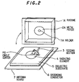
- FIGS.1A to 2 where FIG.1A is a cross sectional view thereof and FIG.1B is an enlarged view showing a part in FIG.1A and FIG.2 is a perspective view showing a radome 1A and the other parts separated of the patch antenna in FIG.1A.
- a microstrip structure is formed by a feeding section 3, a radiating element 4 which are processed of a printed board and a dielectric substrate 5, a grounding conductor 6 which retain the original shape of a printed board.
- a metal patch 2A and the radiating element 4 form a broad- band microstrip antenna.
- the high-frequency wave fed through the feeding section 3 is resonated by the metal patch 2A and the radiating element 4. If the diameter and resonance frequency of the radiating element 4 are D1, f1, respectively, the diameter and resonance frequency of the metal patch 2A are D2, f2, respectively and D2>D1 is given, f1>f2 is obtained.
- a frequency band, which is given by (f1-f2)/f0 is nearly equal to 0.1.
- the radiating element 4 fed though the feeding section 3 resonates near at the frequency f1 and radiates an electric wave.
- the metal patch 2A is electromagnetic-coupled with the radiating element 4, thereby resonating near at the frequency f2 and radiating an electric wave.
- a high-frequency signal with circularly polarized wave electromagnetic field is radiated in the direction of the outer surface 13 of the radome 1A which is made of plastics with a low loss.
- the microstrip structure including the radiating element 4 and the metal patch 2A are covered with the inner surface of the radome 1A and an antenna board 7 on which the microstrip structure is fixed, thereby protected from the external environment of the radome 1A.
- the feeding section 3 and the radiating element 4 are formed on the same surface of a printed board by conductive board etching.
- the metal patch 2A which is made of a thin plate of aluminum and is formed like a disk, receives the circularly polarized wave electromagnetic field at its one surface and then reradiates it from the other surface.
- the other surface of the metal patch 2A is in contact with the inner surface 12 of the radome 1A, and the metal patch 2A is held between the inner surface 12 of the radome 1A and a holder 11A which protrudes from the inner surface 12 and covers a part of the lower surface of the metal patch 2A.
- the holder 11A is formed, as explained after, by processing the tip of a boss 11a.
- the radome 1A is pressed upon the antenna board 7 as it is guided along the circumference of the microstrip structure and is then fixed to the antenna board 7 by screws 8a, 8b.
- the means for fixing the radome 1A to the antenna board 7 is not limited to the screw, and another fixing means by which the position relationship between the radome 1A and the antenna board 7 are precisely determined may be employed.
- the metal patch 2A has a boss hole 21 that is a through-hole penetrating from its one surface to other surface at the center of the surface, i.e., at the position of a circle center P1.
- the inner diameter r of the boss hole 21 is preferably around 5R/100, where R is the outer diameter of the metal patch 2A, taking into account the deterioration in the radiation characteristic of circularly polarized wave electromagnetic field and the holding strength of the metal patch 2A to the radome 1A.
- the metal patch 2A has an outer diameter of R ⁇ 80 mm, a thickness of t ⁇ 0.5 mm and a boss hole inner diameter of r ⁇ 4 mm.
- the holder 11A is formed to cover a part of the lower surface of the metal patch 2A which neighbors on the boss hole 21.
- the holder 11A is a structure which is obtained by processing the tip of the boss 11a that protrudes from the inner surface of the radome 1A.
- the height h of the boss 11a is greater than the thickness t of the metal patch 2A, and the outer diameter r1 of the boss 11a is a little shorter than the inner diameter r of the boss hole 21 of the metal patch 2A.
- the boss 11a is positioned such that the circle center P1 of the metal patch 2A is located, as shown in FIG.1A, just above the circle center P0 of the radiating element 4 when the radome 1A is fixed on the antenna board 7.
- the radome 1A can be made of polycarbonate and the like.
- the thermosoftening temperature(glass transition temperature) Tg where polycarbonate is softened by heating is around 150°C
- crystal-melting temperature Tm where it is fluidized is around 240°C
- heat-resisting temperature where it is used in the solid state is around 125°C.
- FIGS.3A to 3D show a process of fixing the metal patch 2A to the radome 1A in the patch antenna in FIG.1A, where FIGS.3A to 3D correspond to the first to fourth steps, respectively.
- the radome 1A on the inner surface of which protruded is the boss 11a which has a height h greater than the thickness t of the metal patch 2A and has an outer diameter r1 a little shorter than the inner diameter r of the boss hole 21 of the metal patch 2A, is made.
- the metal patch 2A is pressed upon to contact the inner surface 12 as it is guided by the circumference of the boss 11a.
- the tip of the boss 11a is pressed by a hot plate 30 at a temperature higher than the thermosoftening temperature Tg of the boss 11a and lower than the melting temperature Tm of the boss 11a, thereby a part of the boss 11a protruded from the upper surface of the metal patch 2A being softened and formed to provide the holder 11A that has the form to cover a part of the upper surface of the metal patch 2A.
- a disk-like spacer 31 with a thermal resistance is inserted between the hot plate 30 and the metal patch 2A.
- the spacer 31 has a thickness t1 and a hole with a diameter r2 in the center.
- the spacer 31 serves to control the thickness of the holder 11A when pressing the hot plate 30 upon the boss 11a.
- the height h of the boss 11a and the thickness t1 of the spacer 31 is set to give a strength that the thickness and diameter of the resultant holder 11A can sufficiently hold the metal patch 2A, and the diameter r2 of the spacer 31 is set to be greater than a range that the holder 11A extends in the direction of the circumference of the metal patch 2A.
- the hot plate 30 may be substituted by a soldering iron.
- the hot plate 30 and the spacer 31 are removed and the holder 11A is then cooled and hardened, thereby the metal patch 2A being held between the inner surface of the radome 12 and the holder 11A.
- the metal patch 2A can be fixed to the radome 1A by using the fabrication method as shown in FIGS.3A to 3D.
- the radome 1A with the shape shown in FIG.3A can be made by injection molding and the fixing step of the metal patch 2A to the radome 1A by the hot plate 30 is very simple.
- the patch antenna in the first embodiment can be made at a low cost.
- the metal patch 2A can be precisely positioned as it is guided by the boss 11a of the radome 1A which can be precisely formed. Therefore, it is not necessary for the patch antenna in the first embodiment to consider the deterioration in electrical performance caused by the position difference between the metal patch 2A and the radiating element 4.
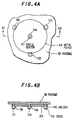
- FIGS.4A and 4B A patch antenna in the second preferred embodiment according to the invention will be explained in FIGS.4A and 4B, where FIG.4A is a plan view thereof and FIG.4B is a cross sectional view cut along the line A1-A2 in FIG.4A.
- the radome 1B further comprises holders 11B, 11C and 11D in addition to the holder 11A of the radome 1A in FIG.1A.
- Each of the holders 11B, 11C and 11D has a form that partially covers the lower surface nearby the circumference of the metal patch 2A, when the metal patch 2A is fixed to the radome 1B.
- the holders 11B, 11C and 11D are, similarly to the holder 11A, formed by thermosoftening and shaping bosses 11b, 11c and 11d(not shown) which are preformed on the radome 1B, respectively, thereafter cooling and hardening them.
- the bosses 11b, 11c and 11d are nearly in contact with the circumference of the metal patch 2A and are protruding from the inner surface 12 of the radome 1B at symmetrical points.
- the holders 11B, 11C and 11D which are made by processing parts of the bosses 11b, 11c and 11d, respectively, are formed to cover the lower surface nearby the circumference of the metal patch 2A.
- the holders 11B, 11C and 11D in addition to the holder 11A, hold the metal patch 2A onto the inner surface 12 of the radome 1B, the holding strength of the metal patch 2A onto the radome 1B can be increased, therefore enhancing the electrical and mechanical stabilities.
- FIGS.5A and 5B A patch antenna in the third preferred embodiment according to the invention will be explained in FIGS.5A and 5B, where FIG.5A is a plan view thereof and FIG.5B is a cross sectional view cut along the line B1-B2 in FIG.5A.
- the radome 1A and the metal patch 2A in the first embodiment as shown in FIG.1A are replaced by a radome 1C and a metal patch 2B, respectively and the other parts in the first embodiment are used as well.
- the fabrication method in the first embodiment can be also used in the third embodiment.
- This patch antenna has a structure that the disk-like metal patch 2B is held onto the inner surface of the radome 1C at its circumference. Namely, there is formed no through-hole at the circle center P2 of the metal patch 2B.
- the radome 1C does not include the holder 11A of the radome 1A as shown in FIG.1A, and it is provided with holders 11E, 11F, 11G and 11H in place of the holder 11A.
- Each of the holders 11E, 11F, 11G and 11H has a form that partially covers the lower surface nearby the circumference of the metal patch 2B, when the metal patch 2B is fixed to the radome 1C.
- the holders 11E, 11F, 11G and 11H are formed by thermosoftening and shaping arc-shaped protrusions 11e, 11f(not shown), 11g and 11h which are preformed on the radome 1C, respectively, thereafter cooling and hardening them.
- the arc-shaped protrusions 11e, 11f, 11g and 11h which are symmetrically formed are protruding from the inner surface 12 of the radome 1C, and the inner walls of the arc-shaped protrusions are nearly in contact with the circumference of the metal patch 2B.
- the holders 11E, 11F, 11G and 11H which are made by processing parts of the arc-shaped protrusions 11e, 11f, 11g and 11h, respectively, are formed to cover the lower surface nearby the circumference of the metal patch 2B.
- the holders 11E, 11F, 11G and 11F hold the metal patch 2B onto the inner surface 12 of the radome 1C, the holding strength of the metal patch 2B onto the radome 1C can be increased, therefore enhancing the electrical and mechanical stabilities.
- the holders 11E, 11F, 11G and 11H are formed as parts of a ring, they may be replaced by an integrated holder which is formed by substituting a ring-shaped protrusion for the arc-shaped protrusions 11e, 11f, 11g and 11h.
- the radome 1C may include a holder nearby the circle center P2 of the metal patch 2B.
Abstract
Description
- This invention relates to a patch antenna, and more particularly to, a patch antenna which has a driven patch with a microstrip structure, a parasitic patch which reradiates an electromagnetic field received from the driven patch and a radome containing these patches to protect them, and a method for making the same.
- It is known that a patch antenna composed of a driven patch and a parasitic patch which are structured as two electromagnetic wave radiating layers has an excellent broad-band performance. By containing such patch antenna inside a radome, a patch antenna structure which presents advantages in terms of portability as mobile communication means, reliability and aesthetical appearance can be provided. For example, such structures are disclosed in Japanese patent application laid-open No.2-141007(1990) and Japanese patent application laid-open No.3-74908(1991), where the former discloses a microstrip antenna in which a parasitic patch is adhered to inner surface of a radome and the latter discloses a stacked microstrip antenna in which a parasitic patch is buried in the wall of a radome.
- However, in the conventional patch antennas disclosed therein, there is a problem that the number of fabrication steps must increase due to requiring the adhesion of the parasitic patch to the radome or the burying of the parasitic patch in the wall of the radome. Also, there is a problem that it is difficult to position the parasitic patch at a proper position on the radome or in the wall of the radome.
- Accordingly, it is an object of the invention to provide a patch antenna in which a parasitic patch is precisely positioned and firmly fixed onto the inner surface of a radome.
- It is a further object of the invention to provide a method for making a patch antenna which facilitates the positioning and fixing of a parasitic patch onto the inner surface of a radome..
- According to the invention, a patch antenna, comprises:
- a driven patch which is fed with a high-frequency signal and radiates a high-frequency electromagnetic field from its one surface;
- a parasitic patch which receives the high-frequency electromagnetic field from the driven patch at its one surface and reradiates the high-frequency electromagnetic field from its other surface; and
- a radome which contains the driven patch and the parasitic patch inside of the radome to protect them and holds the parasitic patch;
wherein the parasitic patch is held by the inner surface of the radome which contacts the other surface of the parasitic patch and a holder which protrudes from the inner surface of the radome and covers a part of the one surface of the parasitic patch. - According to another aspect of the invention, a method for making a patch antenna, which comprises a driven patch which is fed with a high-frequency signal and radiates a high-frequency electromagnetic field from its one surface, a parasitic patch which receives the high-frequency electromagnetic field from the driven patch at its one surface and reradiates the high-frequency electromagnetic field from its other surface, and a radome which contains the driven patch and the parasitic patch inside of the radome to protect them and holds the parasitic patch, comprising the steps of:
- making the radome from which a boss which has a height greater than a thickness of the parasitic patch is protruded at its inner surface;
- pressing the other surface of the parasitic patch to contact the inner surface of radome along the circumferential shape of the boss;
- thermosoftening a part of the boss protruding from the one surface of the parasitic patch and forming it into a shape to cover a part of the one surface of the parasitic patch in order to provide a holder; and
- cooling and hardening the holder to hold the parasitic patch between the radome and the holder.
- The invention will be explained in more detail in conjunction with the appended drawings, wherein:
- FIG.1A is a cross sectional view showing a patch antenna in a first preferred embodiment according to the invention,
- FIG.1B is an enlarged partial view showing the patch antenna in FIG.1A,
- FIG.2 is a perspective view showing the separated state of the patch antenna in the first embodiment,
- FIGS.3A to 3D are cross sectional views showing a method of making a patch antenna in a preferred embodiment according to the invention,
- FIG.4A is a partial plan view showing a patch antenna in a second preferred embodiment according to the invention,
- FIG.4B is a cross sectional view cut along the line A1-A2 in FIG.4A,
- FIG.5A is a partial plan view showing a patch antenna in a third preferred embodiment according to the invention, and
- FIG.5B is a cross sectional view cut along the line B1-B2 in FIG.5A.
- A patch antenna in, the first preferred embodiment will be explained in FIGS.1A to 2, where FIG.1A is a cross sectional view thereof and FIG.1B is an enlarged view showing a part in FIG.1A and FIG.2 is a perspective view showing a
radome 1A and the other parts separated of the patch antenna in FIG.1A. - As shown in FIG.1A and 2, in this patch antenna, a microstrip structure is formed by a
feeding section 3, aradiating element 4 which are processed of a printed board and adielectric substrate 5, agrounding conductor 6 which retain the original shape of a printed board. Ametal patch 2A and the radiatingelement 4 form a broad- band microstrip antenna. The high-frequency wave fed through thefeeding section 3 is resonated by themetal patch 2A and the radiatingelement 4. If the diameter and resonance frequency of theradiating element 4 are D1, f1, respectively, the diameter and resonance frequency of themetal patch 2A are D2, f2, respectively and D2>D1 is given, f1>f2 is obtained. Further, if a center frequency f0 is given by
radiating element 4 fed though thefeeding section 3 resonates near at the frequency f1 and radiates an electric wave. On the other hand, themetal patch 2A is electromagnetic-coupled with theradiating element 4, thereby resonating near at the frequency f2 and radiating an electric wave. As a result, a high-frequency signal with circularly polarized wave electromagnetic field is radiated in the direction of theouter surface 13 of theradome 1A which is made of plastics with a low loss. The microstrip structure including theradiating element 4 and themetal patch 2A are covered with the inner surface of theradome 1A and anantenna board 7 on which the microstrip structure is fixed, thereby protected from the external environment of theradome 1A. - Further explaining this patch antenna in detail, the
feeding section 3 and theradiating element 4 are formed on the same surface of a printed board by conductive board etching. Theradiating element 4, which is formed like a disk, is fed with a phase difference of 90° from two positions with an angle α=90° to each other branched from thefeeding circuit 3. By this feeding, theradiating element 4 radiates the circularly polarized wave electromagnetic field from its one surface. Themetal patch 2A, which is made of a thin plate of aluminum and is formed like a disk, receives the circularly polarized wave electromagnetic field at its one surface and then reradiates it from the other surface. The other surface of themetal patch 2A is in contact with theinner surface 12 of theradome 1A, and themetal patch 2A is held between theinner surface 12 of theradome 1A and aholder 11A which protrudes from theinner surface 12 and covers a part of the lower surface of themetal patch 2A. Theholder 11A is formed, as explained after, by processing the tip of aboss 11a. Theradome 1A is pressed upon theantenna board 7 as it is guided along the circumference of the microstrip structure and is then fixed to theantenna board 7 byscrews 8a, 8b. The means for fixing theradome 1A to theantenna board 7 is not limited to the screw, and another fixing means by which the position relationship between theradome 1A and theantenna board 7 are precisely determined may be employed. - Next, the fixing of the
metal patch 2A to theradome 1A will be explained in detail. Themetal patch 2A has aboss hole 21 that is a through-hole penetrating from its one surface to other surface at the center of the surface, i.e., at the position of a circle center P1. The inner diameter r of theboss hole 21 is preferably around 5R/100, where R is the outer diameter of themetal patch 2A, taking into account the deterioration in the radiation characteristic of circularly polarized wave electromagnetic field and the holding strength of themetal patch 2A to theradome 1A. For example, if the service frequency of the patch antenna is 1.5 GHz to 1.6 GHz, it is suitable that themetal patch 2A has an outer diameter of R≒80 mm, a thickness of t≒0.5 mm and a boss hole inner diameter of r≒4 mm. On theinner surface 12 of theradome 1A, theholder 11A is formed to cover a part of the lower surface of themetal patch 2A which neighbors on theboss hole 21. - The
holder 11A is a structure which is obtained by processing the tip of theboss 11a that protrudes from the inner surface of theradome 1A. The height h of theboss 11a is greater than the thickness t of themetal patch 2A, and the outer diameter r1 of theboss 11a is a little shorter than the inner diameter r of theboss hole 21 of themetal patch 2A. Theboss 11a is positioned such that the circle center P1 of themetal patch 2A is located, as shown in FIG.1A, just above the circle center P0 of theradiating element 4 when theradome 1A is fixed on theantenna board 7. After the upper surface of themetal patch 2A is pressed upon theinner surface 12 of theradome 1A as themetal patch 2A is guided by theboss 11a, the tip of theboss 11a is softened by heating and compressed in the direction of theinner surface 12, thereby transformed into a form to cover a part of the lower surface of themetal patch 2A, then cooled and hardened to provide theholder 11A as shown. Theradome 1A can be made of polycarbonate and the like. The thermosoftening temperature(glass transition temperature) Tg where polycarbonate is softened by heating is around 150°C, crystal-melting temperature Tm where it is fluidized is around 240°C and heat-resisting temperature where it is used in the solid state is around 125°C. - FIGS.3A to 3D show a process of fixing the
metal patch 2A to theradome 1A in the patch antenna in FIG.1A, where FIGS.3A to 3D correspond to the first to fourth steps, respectively. - In the first step, the
radome 1A, on the inner surface of which protruded is theboss 11a which has a height h greater than the thickness t of themetal patch 2A and has an outer diameter r1 a little shorter than the inner diameter r of theboss hole 21 of themetal patch 2A, is made. In the second step, themetal patch 2A is pressed upon to contact theinner surface 12 as it is guided by the circumference of theboss 11a. - In the third step, the tip of the
boss 11a is pressed by ahot plate 30 at a temperature higher than the thermosoftening temperature Tg of theboss 11a and lower than the melting temperature Tm of theboss 11a, thereby a part of theboss 11a protruded from the upper surface of themetal patch 2A being softened and formed to provide theholder 11A that has the form to cover a part of the upper surface of themetal patch 2A. Here, between thehot plate 30 and themetal patch 2A, a disk-like spacer 31 with a thermal resistance is inserted. Thespacer 31 has a thickness t1 and a hole with a diameter r2 in the center. Thespacer 31 serves to control the thickness of theholder 11A when pressing thehot plate 30 upon theboss 11a. The height h of theboss 11a and the thickness t1 of thespacer 31 is set to give a strength that the thickness and diameter of theresultant holder 11A can sufficiently hold themetal patch 2A, and the diameter r2 of thespacer 31 is set to be greater than a range that theholder 11A extends in the direction of the circumference of themetal patch 2A. Thehot plate 30 may be substituted by a soldering iron. - In the fourth step, the
hot plate 30 and thespacer 31 are removed and theholder 11A is then cooled and hardened, thereby themetal patch 2A being held between the inner surface of theradome 12 and theholder 11A. - As explained above, in the first embodiment, the
metal patch 2A can be fixed to theradome 1A by using the fabrication method as shown in FIGS.3A to 3D. Theradome 1A with the shape shown in FIG.3A can be made by injection molding and the fixing step of themetal patch 2A to theradome 1A by thehot plate 30 is very simple. Thus, the patch antenna in the first embodiment can be made at a low cost. - Furthermore, the
metal patch 2A can be precisely positioned as it is guided by theboss 11a of theradome 1A which can be precisely formed. Therefore, it is not necessary for the patch antenna in the first embodiment to consider the deterioration in electrical performance caused by the position difference between themetal patch 2A and theradiating element 4. - A patch antenna in the second preferred embodiment according to the invention will be explained in FIGS.4A and 4B, where FIG.4A is a plan view thereof and FIG.4B is a cross sectional view cut along the line A1-A2 in FIG.4A.
- In the second embodiment, only the
radome 1A in the first embodiment as shown in FIG.1A is replaced by aradome 1B and the other parts in the first embodiment are used as well. The fabrication method in the first embodiment can be also used in the second embodiment. Theradome 1B further comprisesholders holder 11A of theradome 1A in FIG.1A. Each of theholders metal patch 2A, when themetal patch 2A is fixed to theradome 1B. Theholders holder 11A, formed by thermosoftening and shapingbosses radome 1B, respectively, thereafter cooling and hardening them. Thebosses metal patch 2A and are protruding from theinner surface 12 of theradome 1B at symmetrical points. By processing thebosses holders bosses metal patch 2A. In the second embodiment, since theholders holder 11A, hold themetal patch 2A onto theinner surface 12 of theradome 1B, the holding strength of themetal patch 2A onto theradome 1B can be increased, therefore enhancing the electrical and mechanical stabilities. - A patch antenna in the third preferred embodiment according to the invention will be explained in FIGS.5A and 5B, where FIG.5A is a plan view thereof and FIG.5B is a cross sectional view cut along the line B1-B2 in FIG.5A.
- In the third embodiment, the
radome 1A and themetal patch 2A in the first embodiment as shown in FIG.1A are replaced by aradome 1C and ametal patch 2B, respectively and the other parts in the first embodiment are used as well. The fabrication method in the first embodiment can be also used in the third embodiment. This patch antenna has a structure that the disk-like metal patch 2B is held onto the inner surface of theradome 1C at its circumference. Namely, there is formed no through-hole at the circle center P2 of themetal patch 2B. Also, theradome 1C does not include theholder 11A of theradome 1A as shown in FIG.1A, and it is provided withholders holder 11A. Each of theholders metal patch 2B, when themetal patch 2B is fixed to theradome 1C. - The
holders radome 1C, respectively, thereafter cooling and hardening them. The arc-shapedprotrusions inner surface 12 of theradome 1C, and the inner walls of the arc-shaped protrusions are nearly in contact with the circumference of themetal patch 2B. Theholders protrusions metal patch 2B. In the third embodiment, since theholders metal patch 2B onto theinner surface 12 of theradome 1C, the holding strength of themetal patch 2B onto theradome 1C can be increased, therefore enhancing the electrical and mechanical stabilities. - Though, in the third embodiment, the
holders protrusions radome 1C may include a holder nearby the circle center P2 of themetal patch 2B. - Although the invention has been described with respect to specific embodiment for complete and clear disclosure, the appended claims are not to be thus limited but are to be construed as embodying all modification and alternative constructions that may be occurred to one skilled in the art which fairly fall within the basic teaching here is set forth.
Claims (7)
- A patch antenna, comprising:a driven patch which is fed with a high-frequency signal and radiates a high-frequency electromagnetic field from its one surface;a parasitic patch which receives said high-frequency electromagnetic field from said driven patch at its one surface and reradiates said high-frequency electromagnetic field from its other surface; anda radome which contains said driven patch and said parasitic patch inside of said radome to protect them and holds said parasitic patch;
wherein said parasitic patch is held by the inner surface of said radome which contacts said other surface of said parasitic patch and a holder which protrudes from said inner surface of said radome and covers a part of said one surface of said parasitic patch. - A patch antenna, according to claim 1, wherein:said parasitic patch has a through-hole at the center of its surface, andsaid holder of said radome comprises a first holding member which penetrates said through-hole of said parasitic patch from said inner surface of said radome and covers said one surface of said parasitic patch nearby said through-hole.
- A patch antenna, according to claim 2, wherein:said holder of said radome further comprises one or a plurality of second holding members which cover a part of the circumference of said parasitic patch.
- A patch antenna, according to any of claims 1 to 3, wherein:said holder of said radome covers a part or all of the circumference of said parasitic patch.
- A patch antenna, according to any of claims 1 to 4, wherein:said holder is formed by thermosoftening, shaping, cooling and then hardening its tip after positioning said other surface of said parasitic patch onto said inner surface of said radome.
- A patch antenna, according to claim 5, wherein:said parasitic patch is positioned as it is guided by said holder before said thermosoftening.
- A method for making a patch antenna, which comprises a driven patch which is fed with a high-frequency signal and radiates a high-frequency electromagnetic field from its one surface, a parasitic patch which receives said high-frequency electromagnetic field from said driven patch at its one surface and reradiates said high-frequency electromagnetic field from its other surface, and a radome which contains said driven patch and said parasitic patch inside of said radome to protect them and holds said parasitic patch, comprising the steps of:making said radome from which a boss which has a height greater than a thickness of said parasitic patch is protruded at its inner surface;pressing said other surface of said parasitic patch to contact said inner surface of radome along the circumferential shape of said boss;thermosoftening a part of said boss protruding from said one surface of said parasitic patch and forming it into a shape to cover a part of said one surface of said parasitic patch in order to provide a holder; andcooling and hardening said holder to hold said parasitic patch between said radome and said holder.
Applications Claiming Priority (3)
| Application Number | Priority Date | Filing Date | Title |
|---|---|---|---|
| JP8052719A JP2957463B2 (en) | 1996-03-11 | 1996-03-11 | Patch antenna and method of manufacturing the same |
| JP5271996 | 1996-03-11 | ||
| JP52719/96 | 1996-03-11 |
Publications (3)
| Publication Number | Publication Date |
|---|---|
| EP0795925A2 true EP0795925A2 (en) | 1997-09-17 |
| EP0795925A3 EP0795925A3 (en) | 1998-01-14 |
| EP0795925B1 EP0795925B1 (en) | 2001-11-21 |
Family
ID=12922737
Family Applications (1)
| Application Number | Title | Priority Date | Filing Date |
|---|---|---|---|
| EP97103971A Expired - Lifetime EP0795925B1 (en) | 1996-03-11 | 1997-03-10 | Patch antenna and method for making the same |
Country Status (7)
| Country | Link |
|---|---|
| US (1) | US5977710A (en) |
| EP (1) | EP0795925B1 (en) |
| JP (1) | JP2957463B2 (en) |
| CN (1) | CN1078754C (en) |
| AU (1) | AU726672B2 (en) |
| CA (1) | CA2199581C (en) |
| DE (1) | DE69708358T2 (en) |
Cited By (7)
| Publication number | Priority date | Publication date | Assignee | Title |
|---|---|---|---|---|
| WO2000036703A1 (en) * | 1998-12-11 | 2000-06-22 | Robert Bosch Gmbh | Half-loop antenna |
| EP1133001A2 (en) * | 2000-03-09 | 2001-09-12 | Alps Electric Co., Ltd. | Wideband antenna mountable in vehicle cabin |
| WO2006061307A1 (en) * | 2004-12-09 | 2006-06-15 | Robert Bosch Gmbh | Antenna assembly for a radar transceiver |
| WO2006072511A1 (en) * | 2004-12-30 | 2006-07-13 | Robert Bosch Gmbh | Antenna array for a radar transceiver |
| WO2007047002A2 (en) * | 2005-09-15 | 2007-04-26 | Qualcomm Incorporated | On a radome mounted gps antenna assembly |
| WO2007062971A1 (en) * | 2005-11-29 | 2007-06-07 | Robert Bosch Gmbh | Antenna array for a radar sensor |
| US8038815B2 (en) | 2007-07-17 | 2011-10-18 | Qualcomm Incorporated | Fluorescent dye to improve primer coverage accuracy for bonding applications |
Families Citing this family (73)
| Publication number | Priority date | Publication date | Assignee | Title |
|---|---|---|---|---|
| US6366244B1 (en) * | 1993-03-11 | 2002-04-02 | Southern California Edison Company | Planar dual band microstrip or slotted waveguide array antenna for all weather applications |
| US5734350A (en) * | 1996-04-08 | 1998-03-31 | Xertex Technologies, Inc. | Microstrip wide band antenna |
| US6236367B1 (en) | 1998-09-25 | 2001-05-22 | Deltec Telesystems International Limited | Dual polarised patch-radiating element |
| US6421011B1 (en) * | 1999-10-22 | 2002-07-16 | Lucent Technologies Inc. | Patch antenna using non-conductive frame |
| US6404389B1 (en) * | 1999-10-22 | 2002-06-11 | Lucent Technologies Inc. | Patch antenna |
| US6407704B1 (en) * | 1999-10-22 | 2002-06-18 | Lucent Technologies Inc. | Patch antenna using non-conductive thermo form frame |
| WO2002063716A1 (en) * | 2001-02-06 | 2002-08-15 | Harris Corporation | Split pole mounting of unprotected microwave radio with parabolic antenna |
| US7071883B2 (en) * | 2001-07-11 | 2006-07-04 | Eagle Broadband, Inc. | Set-top box having an improved patch antenna |
| JP2004077399A (en) * | 2002-08-22 | 2004-03-11 | Hitachi Ltd | Milliwave radar |
| WO2004038862A1 (en) * | 2002-10-25 | 2004-05-06 | National Institute Of Information And Communications Technology | Antenna device |
| DE10318815A1 (en) * | 2003-04-17 | 2004-11-04 | Valeo Schalter Und Sensoren Gmbh | Slot-coupled radar antenna with radiation areas |
| JP2005012376A (en) * | 2003-06-17 | 2005-01-13 | Mitsumi Electric Co Ltd | Antenna device |
| JP2005073168A (en) * | 2003-08-27 | 2005-03-17 | Uniden Corp | Reradiation antenna system |
| KR100542829B1 (en) * | 2003-09-09 | 2006-01-20 | 한국전자통신연구원 | High Gain and Wideband Microstrip Patch Antenna for Transmitting/Receiving and Array Antenna Arraying it |
| US7167128B1 (en) * | 2003-10-03 | 2007-01-23 | Sirius Satellite Radio, Inc. | Modular patch antenna providing antenna gain direction selection capability |
| DE102005005781A1 (en) * | 2005-02-08 | 2006-08-10 | Kathrein-Werke Kg | Radom, in particular for mobile radio antennas and associated mobile radio antenna |
| EP1854170B8 (en) | 2005-02-11 | 2018-10-17 | Meggitt SA | Microstrip patch antenna for high temperature environments |
| FI20055420A0 (en) | 2005-07-25 | 2005-07-25 | Lk Products Oy | Adjustable multi-band antenna |
| US7304612B2 (en) * | 2005-08-10 | 2007-12-04 | Navini Networks, Inc. | Microstrip antenna with integral feed and antenna structures |
| FI119009B (en) | 2005-10-03 | 2008-06-13 | Pulse Finland Oy | Multiple-band antenna |
| FI118782B (en) | 2005-10-14 | 2008-03-14 | Pulse Finland Oy | Adjustable antenna |
| DE102005054286B4 (en) * | 2005-11-11 | 2011-04-07 | Delphi Delco Electronics Europe Gmbh | antenna array |
| CN101038983B (en) * | 2006-03-13 | 2012-09-05 | 中国科学院电子学研究所 | Variable frequency coupling feeder apparatus for wide-band microstrip aerial |
| CN101098037B (en) * | 2006-06-26 | 2012-06-13 | 耀登科技股份有限公司 | Method for producing paster type antenna |
| US8618990B2 (en) | 2011-04-13 | 2013-12-31 | Pulse Finland Oy | Wideband antenna and methods |
| US7505002B2 (en) * | 2006-12-04 | 2009-03-17 | Agc Automotive Americas R&D, Inc. | Beam tilting patch antenna using higher order resonance mode |
| US20080129635A1 (en) * | 2006-12-04 | 2008-06-05 | Agc Automotive Americas R&D, Inc. | Method of operating a patch antenna in a higher order mode |
| FI20075269A0 (en) | 2007-04-19 | 2007-04-19 | Pulse Finland Oy | Method and arrangement for antenna matching |
| US20090027298A1 (en) * | 2007-07-24 | 2009-01-29 | Symbol Technologies, Inc. | Antenna Radome With Integrated Director Element |
| FI120427B (en) | 2007-08-30 | 2009-10-15 | Pulse Finland Oy | Adjustable multiband antenna |
| US7696930B2 (en) * | 2008-04-14 | 2010-04-13 | International Business Machines Corporation | Radio frequency (RF) integrated circuit (IC) packages with integrated aperture-coupled patch antenna(s) in ring and/or offset cavities |
| US8045329B2 (en) * | 2009-04-29 | 2011-10-25 | Raytheon Company | Thermal dissipation mechanism for an antenna |
| FI20096134A0 (en) | 2009-11-03 | 2009-11-03 | Pulse Finland Oy | Adjustable antenna |
| FI20096251A0 (en) | 2009-11-27 | 2009-11-27 | Pulse Finland Oy | MIMO antenna |
| US8847833B2 (en) | 2009-12-29 | 2014-09-30 | Pulse Finland Oy | Loop resonator apparatus and methods for enhanced field control |
| FI20105158A (en) | 2010-02-18 | 2011-08-19 | Pulse Finland Oy | SHELL RADIATOR ANTENNA |
| CN102332635B (en) * | 2010-04-07 | 2013-12-25 | 庄昆杰 | Small-sized multi-band and high-grain dual polarization microstrip antenna at microwave low band |
| US9406998B2 (en) | 2010-04-21 | 2016-08-02 | Pulse Finland Oy | Distributed multiband antenna and methods |
| FI20115072A0 (en) | 2011-01-25 | 2011-01-25 | Pulse Finland Oy | Multi-resonance antenna, antenna module and radio unit |
| US8648752B2 (en) | 2011-02-11 | 2014-02-11 | Pulse Finland Oy | Chassis-excited antenna apparatus and methods |
| US9673507B2 (en) | 2011-02-11 | 2017-06-06 | Pulse Finland Oy | Chassis-excited antenna apparatus and methods |
| US8866689B2 (en) | 2011-07-07 | 2014-10-21 | Pulse Finland Oy | Multi-band antenna and methods for long term evolution wireless system |
| US9450291B2 (en) | 2011-07-25 | 2016-09-20 | Pulse Finland Oy | Multiband slot loop antenna apparatus and methods |
| US9123990B2 (en) | 2011-10-07 | 2015-09-01 | Pulse Finland Oy | Multi-feed antenna apparatus and methods |
| US9531058B2 (en) | 2011-12-20 | 2016-12-27 | Pulse Finland Oy | Loosely-coupled radio antenna apparatus and methods |
| US9484619B2 (en) | 2011-12-21 | 2016-11-01 | Pulse Finland Oy | Switchable diversity antenna apparatus and methods |
| US8988296B2 (en) | 2012-04-04 | 2015-03-24 | Pulse Finland Oy | Compact polarized antenna and methods |
| US9225070B1 (en) * | 2012-10-01 | 2015-12-29 | Lockheed Martin Corporation | Cavity backed aperture coupled dielectrically loaded waveguide radiating element with even mode excitation and wide angle impedance matching |
| US9979078B2 (en) | 2012-10-25 | 2018-05-22 | Pulse Finland Oy | Modular cell antenna apparatus and methods |
| US10069209B2 (en) | 2012-11-06 | 2018-09-04 | Pulse Finland Oy | Capacitively coupled antenna apparatus and methods |
| US10079428B2 (en) | 2013-03-11 | 2018-09-18 | Pulse Finland Oy | Coupled antenna structure and methods |
| US9647338B2 (en) | 2013-03-11 | 2017-05-09 | Pulse Finland Oy | Coupled antenna structure and methods |
| US9634383B2 (en) | 2013-06-26 | 2017-04-25 | Pulse Finland Oy | Galvanically separated non-interacting antenna sector apparatus and methods |
| US9680212B2 (en) | 2013-11-20 | 2017-06-13 | Pulse Finland Oy | Capacitive grounding methods and apparatus for mobile devices |
| US9590308B2 (en) | 2013-12-03 | 2017-03-07 | Pulse Electronics, Inc. | Reduced surface area antenna apparatus and mobile communications devices incorporating the same |
| US9350081B2 (en) | 2014-01-14 | 2016-05-24 | Pulse Finland Oy | Switchable multi-radiator high band antenna apparatus |
| JP6354267B2 (en) * | 2014-04-01 | 2018-07-11 | 株式会社デンソーウェーブ | Antenna device and communication device |
| US9948002B2 (en) | 2014-08-26 | 2018-04-17 | Pulse Finland Oy | Antenna apparatus with an integrated proximity sensor and methods |
| US9973228B2 (en) | 2014-08-26 | 2018-05-15 | Pulse Finland Oy | Antenna apparatus with an integrated proximity sensor and methods |
| US9722308B2 (en) | 2014-08-28 | 2017-08-01 | Pulse Finland Oy | Low passive intermodulation distributed antenna system for multiple-input multiple-output systems and methods of use |
| US9906260B2 (en) | 2015-07-30 | 2018-02-27 | Pulse Finland Oy | Sensor-based closed loop antenna swapping apparatus and methods |
| GB2556185A (en) | 2016-09-26 | 2018-05-23 | Taoglas Group Holdings Ltd | Patch antenna construction |
| JP6597659B2 (en) * | 2017-02-01 | 2019-10-30 | 株式会社村田製作所 | ANTENNA DEVICE AND ANTENNA DEVICE MANUFACTURING METHOD |
| US10971806B2 (en) | 2017-08-22 | 2021-04-06 | The Boeing Company | Broadband conformal antenna |
| US10910706B2 (en) * | 2018-01-19 | 2021-02-02 | Mediatek Inc. | Radar sensor housing design |
| US11233310B2 (en) * | 2018-01-29 | 2022-01-25 | The Boeing Company | Low-profile conformal antenna |
| US20200021010A1 (en) * | 2018-07-13 | 2020-01-16 | Qualcomm Incorporated | Air coupled superstrate antenna on device housing |
| US10916853B2 (en) | 2018-08-24 | 2021-02-09 | The Boeing Company | Conformal antenna with enhanced circular polarization |
| US10923831B2 (en) | 2018-08-24 | 2021-02-16 | The Boeing Company | Waveguide-fed planar antenna array with enhanced circular polarization |
| US10938082B2 (en) | 2018-08-24 | 2021-03-02 | The Boeing Company | Aperture-coupled microstrip-to-waveguide transitions |
| DE102018218891B4 (en) | 2018-11-06 | 2023-12-07 | Fraunhofer-Gesellschaft zur Förderung der angewandten Forschung e.V. | Three-dimensional loop antenna device |
| JPWO2021066140A1 (en) * | 2019-10-02 | 2021-04-08 | ||
| US11276933B2 (en) | 2019-11-06 | 2022-03-15 | The Boeing Company | High-gain antenna with cavity between feed line and ground plane |
Citations (5)
| Publication number | Priority date | Publication date | Assignee | Title |
|---|---|---|---|---|
| EP0366593A2 (en) * | 1988-10-28 | 1990-05-02 | Emerson Electric Co. | Method of ultrasonically assembling workpieces |
| EP0394489A1 (en) * | 1988-10-19 | 1990-10-31 | Toyo Communication Equipment Co. Ltd. | Array antenna and a feeder device therefor |
| US4987421A (en) * | 1988-06-09 | 1991-01-22 | Mitsubishi Denki Kabushiki Kaisha | Microstrip antenna |
| EP0618061A2 (en) * | 1993-03-24 | 1994-10-05 | Nhk Spring Co.Ltd. | Method for crimping a thermoplastic resin member and assembly including a thus crimped thermoplastic resin member |
| EP0629785A2 (en) * | 1993-06-01 | 1994-12-21 | TOHOKU MUNEKATA Co., Ltd. | Mounting components in plastic casings |
Family Cites Families (15)
| Publication number | Priority date | Publication date | Assignee | Title |
|---|---|---|---|---|
| JPH0221221Y2 (en) * | 1985-06-27 | 1990-06-08 | ||
| JPS625917A (en) * | 1985-07-03 | 1987-01-12 | Airin:Kk | Production of saponin containing no isoflavone from soybean embro bud |
| JPS62228705A (en) * | 1986-03-31 | 1987-10-07 | 東芝テック株式会社 | Method of fixing member |
| JPS61281605A (en) * | 1986-06-20 | 1986-12-12 | Hitachi Ltd | Phased array antenna |
| JPH02141007A (en) * | 1988-11-21 | 1990-05-30 | Mitsubishi Electric Corp | Micro-strip antenna |
| JPH0374908A (en) * | 1989-08-16 | 1991-03-29 | Toyo Commun Equip Co Ltd | Microstrip antenna of stack type |
| JP2749398B2 (en) * | 1989-10-06 | 1998-05-13 | 株式会社アマダ | Work transfer device |
| JPH0777291B2 (en) * | 1990-07-25 | 1995-08-16 | 日立電線株式会社 | Method for manufacturing molded circuit board |
| JPH0471011U (en) * | 1990-10-31 | 1992-06-23 | ||
| US5231406A (en) * | 1991-04-05 | 1993-07-27 | Ball Corporation | Broadband circular polarization satellite antenna |
| US5210542A (en) * | 1991-07-03 | 1993-05-11 | Ball Corporation | Microstrip patch antenna structure |
| JPH05167332A (en) * | 1991-12-13 | 1993-07-02 | Matsushita Electric Works Ltd | Antenna for mobile object communication |
| JP3500524B2 (en) * | 1993-12-16 | 2004-02-23 | マスプロ電工株式会社 | Mobile satellite communication antenna |
| JPH08139522A (en) * | 1994-09-13 | 1996-05-31 | Matsushita Electric Works Ltd | Compound antenna and antenna unit |
| JP3121716U (en) * | 2006-03-06 | 2006-05-25 | クボタ貿易株式会社 | Glass built ossuary |
-
1996
- 1996-03-11 JP JP8052719A patent/JP2957463B2/en not_active Expired - Fee Related
-
1997
- 1997-03-10 CA CA002199581A patent/CA2199581C/en not_active Expired - Fee Related
- 1997-03-10 DE DE69708358T patent/DE69708358T2/en not_active Expired - Fee Related
- 1997-03-10 EP EP97103971A patent/EP0795925B1/en not_active Expired - Lifetime
- 1997-03-11 CN CN97100630A patent/CN1078754C/en not_active Expired - Fee Related
- 1997-03-11 US US08/814,343 patent/US5977710A/en not_active Expired - Fee Related
- 1997-03-11 AU AU16207/97A patent/AU726672B2/en not_active Ceased
Patent Citations (5)
| Publication number | Priority date | Publication date | Assignee | Title |
|---|---|---|---|---|
| US4987421A (en) * | 1988-06-09 | 1991-01-22 | Mitsubishi Denki Kabushiki Kaisha | Microstrip antenna |
| EP0394489A1 (en) * | 1988-10-19 | 1990-10-31 | Toyo Communication Equipment Co. Ltd. | Array antenna and a feeder device therefor |
| EP0366593A2 (en) * | 1988-10-28 | 1990-05-02 | Emerson Electric Co. | Method of ultrasonically assembling workpieces |
| EP0618061A2 (en) * | 1993-03-24 | 1994-10-05 | Nhk Spring Co.Ltd. | Method for crimping a thermoplastic resin member and assembly including a thus crimped thermoplastic resin member |
| EP0629785A2 (en) * | 1993-06-01 | 1994-12-21 | TOHOKU MUNEKATA Co., Ltd. | Mounting components in plastic casings |
Non-Patent Citations (3)
| Title |
|---|
| PATENT ABSTRACTS OF JAPAN vol. 014, no. 383 (E-0966), 17 August 1990 & JP 02 141007 A (MITSUBISHI ELECTRIC CORP), 30 May 1990, * |
| PATENT ABSTRACTS OF JAPAN vol. 015, no. 241 (E-1080), 21 June 1991 & JP 03 074908 A (TOYO COMMUN EQUIP CO LTD), 29 March 1991, * |
| PATENT ABSTRACTS OF JAPAN vol. 095, no. 010, 30 November 1995 & JP 07 176925 A (MASPRO DENKOH CORP), 14 July 1995, * |
Cited By (13)
| Publication number | Priority date | Publication date | Assignee | Title |
|---|---|---|---|---|
| US6590541B1 (en) | 1998-12-11 | 2003-07-08 | Robert Bosch Gmbh | Half-loop antenna |
| WO2000036703A1 (en) * | 1998-12-11 | 2000-06-22 | Robert Bosch Gmbh | Half-loop antenna |
| EP1133001A2 (en) * | 2000-03-09 | 2001-09-12 | Alps Electric Co., Ltd. | Wideband antenna mountable in vehicle cabin |
| EP1133001A3 (en) * | 2000-03-09 | 2003-07-30 | Alps Electric Co., Ltd. | Wideband antenna mountable in vehicle cabin |
| WO2006061307A1 (en) * | 2004-12-09 | 2006-06-15 | Robert Bosch Gmbh | Antenna assembly for a radar transceiver |
| US7671806B2 (en) | 2004-12-30 | 2010-03-02 | Robert Bosch Gmbh | Antenna system for a radar transceiver |
| WO2006072511A1 (en) * | 2004-12-30 | 2006-07-13 | Robert Bosch Gmbh | Antenna array for a radar transceiver |
| WO2007047002A2 (en) * | 2005-09-15 | 2007-04-26 | Qualcomm Incorporated | On a radome mounted gps antenna assembly |
| WO2007047002A3 (en) * | 2005-09-15 | 2007-07-05 | Qualcomm Inc | On a radome mounted gps antenna assembly |
| US7336241B2 (en) | 2005-09-15 | 2008-02-26 | Qualcomm Incorporated | GPS radome-mounted antenna assembly |
| WO2007062971A1 (en) * | 2005-11-29 | 2007-06-07 | Robert Bosch Gmbh | Antenna array for a radar sensor |
| US8038815B2 (en) | 2007-07-17 | 2011-10-18 | Qualcomm Incorporated | Fluorescent dye to improve primer coverage accuracy for bonding applications |
| US8410992B2 (en) | 2007-07-17 | 2013-04-02 | Qualcomm Incorporated | Fluorescent dye to improve primer coverage accuracy for bonding applications |
Also Published As
| Publication number | Publication date |
|---|---|
| JPH09246851A (en) | 1997-09-19 |
| EP0795925B1 (en) | 2001-11-21 |
| AU726672B2 (en) | 2000-11-16 |
| CN1164134A (en) | 1997-11-05 |
| CN1078754C (en) | 2002-01-30 |
| JP2957463B2 (en) | 1999-10-04 |
| US5977710A (en) | 1999-11-02 |
| CA2199581C (en) | 2000-05-02 |
| DE69708358D1 (en) | 2002-01-03 |
| DE69708358T2 (en) | 2002-07-18 |
| AU1620797A (en) | 1997-09-18 |
| CA2199581A1 (en) | 1997-09-11 |
| EP0795925A3 (en) | 1998-01-14 |
Similar Documents
| Publication | Publication Date | Title |
|---|---|---|
| EP0795925B1 (en) | Patch antenna and method for making the same | |
| KR101982030B1 (en) | Antenna device and method for manufacturing antenna device | |
| EP0278070B1 (en) | Circular microstrip vehicular rf antenna | |
| US4724443A (en) | Patch antenna with a strip line feed element | |
| EP0332139B1 (en) | Wide band antenna for mobile communications | |
| JP3788115B2 (en) | Method for manufacturing antenna device | |
| WO2001041256A1 (en) | An antenna assembly and a method of mounting an antenna assembly | |
| WO1998027609A1 (en) | Small omni-directional, slot antenna | |
| US20040021606A1 (en) | Small plane antenna and composite antenna using the same | |
| US7079078B2 (en) | Patch antenna apparatus preferable for receiving ground wave and signal wave from low elevation angle satellite | |
| JP2001326506A (en) | Array antenna | |
| KR102228689B1 (en) | Antenna device and manufacturing method thereof | |
| US20080055183A1 (en) | Antenna apparatus | |
| CN112968267B (en) | Electronic equipment | |
| CN112117540B (en) | Electronic device | |
| JP2956598B2 (en) | Planar antenna | |
| US7557679B2 (en) | Sealed microwave feedthrough | |
| JPH07288420A (en) | Dual band antenna | |
| KR19990084408A (en) | Planar antenna using multilayer dielectric with air layer | |
| JP2004048367A (en) | Composite antenna | |
| CN217881884U (en) | Antenna module and communication equipment | |
| KR102139075B1 (en) | Electronic device with slot antenna | |
| JP3147609B2 (en) | Antenna and resonance frequency adjusting method thereof | |
| JPH0936646A (en) | Method for adjusting resonance frequency of microstrip antenna | |
| JPH0936648A (en) | Method for adjusting resonance frequency of microstrip antenna |
Legal Events
| Date | Code | Title | Description |
|---|---|---|---|
| PUAI | Public reference made under article 153(3) epc to a published international application that has entered the european phase |
Free format text: ORIGINAL CODE: 0009012 |
|
| AK | Designated contracting states |
Kind code of ref document: A2 Designated state(s): DE FR GB IT NL |
|
| PUAL | Search report despatched |
Free format text: ORIGINAL CODE: 0009013 |
|
| AK | Designated contracting states |
Kind code of ref document: A3 Designated state(s): DE FR GB IT NL |
|
| 17P | Request for examination filed |
Effective date: 19971203 |
|
| 17Q | First examination report despatched |
Effective date: 19990125 |
|
| GRAG | Despatch of communication of intention to grant |
Free format text: ORIGINAL CODE: EPIDOS AGRA |
|
| GRAG | Despatch of communication of intention to grant |
Free format text: ORIGINAL CODE: EPIDOS AGRA |
|
| GRAH | Despatch of communication of intention to grant a patent |
Free format text: ORIGINAL CODE: EPIDOS IGRA |
|
| GRAH | Despatch of communication of intention to grant a patent |
Free format text: ORIGINAL CODE: EPIDOS IGRA |
|
| GRAA | (expected) grant |
Free format text: ORIGINAL CODE: 0009210 |
|
| AK | Designated contracting states |
Kind code of ref document: B1 Designated state(s): DE FR GB IT NL |
|
| REG | Reference to a national code |
Ref country code: GB Ref legal event code: IF02 |
|
| REF | Corresponds to: |
Ref document number: 69708358 Country of ref document: DE Date of ref document: 20020103 |
|
| ET | Fr: translation filed | ||
| PLBE | No opposition filed within time limit |
Free format text: ORIGINAL CODE: 0009261 |
|
| STAA | Information on the status of an ep patent application or granted ep patent |
Free format text: STATUS: NO OPPOSITION FILED WITHIN TIME LIMIT |
|
| 26N | No opposition filed | ||
| PGFP | Annual fee paid to national office [announced via postgrant information from national office to epo] |
Ref country code: NL Payment date: 20090315 Year of fee payment: 13 |
|
| PGFP | Annual fee paid to national office [announced via postgrant information from national office to epo] |
Ref country code: GB Payment date: 20090304 Year of fee payment: 13 |
|
| PGFP | Annual fee paid to national office [announced via postgrant information from national office to epo] |
Ref country code: IT Payment date: 20090319 Year of fee payment: 13 Ref country code: DE Payment date: 20090306 Year of fee payment: 13 |
|
| PGFP | Annual fee paid to national office [announced via postgrant information from national office to epo] |
Ref country code: FR Payment date: 20090316 Year of fee payment: 13 |
|
| REG | Reference to a national code |
Ref country code: NL Ref legal event code: V1 Effective date: 20101001 |
|
| GBPC | Gb: european patent ceased through non-payment of renewal fee |
Effective date: 20100310 |
|
| REG | Reference to a national code |
Ref country code: FR Ref legal event code: ST Effective date: 20101130 |
|
| PG25 | Lapsed in a contracting state [announced via postgrant information from national office to epo] |
Ref country code: NL Free format text: LAPSE BECAUSE OF NON-PAYMENT OF DUE FEES Effective date: 20101001 Ref country code: FR Free format text: LAPSE BECAUSE OF NON-PAYMENT OF DUE FEES Effective date: 20100331 |
|
| PG25 | Lapsed in a contracting state [announced via postgrant information from national office to epo] |
Ref country code: DE Free format text: LAPSE BECAUSE OF NON-PAYMENT OF DUE FEES Effective date: 20101001 |
|
| PG25 | Lapsed in a contracting state [announced via postgrant information from national office to epo] |
Ref country code: GB Free format text: LAPSE BECAUSE OF NON-PAYMENT OF DUE FEES Effective date: 20100310 Ref country code: IT Free format text: LAPSE BECAUSE OF NON-PAYMENT OF DUE FEES Effective date: 20100310 |