EP0794684B1 - Optisches Paketvermittlungssystem - Google Patents
Optisches Paketvermittlungssystem Download PDFInfo
- Publication number
- EP0794684B1 EP0794684B1 EP97200571A EP97200571A EP0794684B1 EP 0794684 B1 EP0794684 B1 EP 0794684B1 EP 97200571 A EP97200571 A EP 97200571A EP 97200571 A EP97200571 A EP 97200571A EP 0794684 B1 EP0794684 B1 EP 0794684B1
- Authority
- EP
- European Patent Office
- Prior art keywords
- polarisation
- signal
- packet
- optical
- address
- Prior art date
- Legal status (The legal status is an assumption and is not a legal conclusion. Google has not performed a legal analysis and makes no representation as to the accuracy of the status listed.)
- Expired - Lifetime
Links
- 230000003287 optical effect Effects 0.000 title claims abstract description 121
- 230000005540 biological transmission Effects 0.000 claims description 30
- 230000004048 modification Effects 0.000 claims description 6
- 238000012986 modification Methods 0.000 claims description 6
- 238000006243 chemical reaction Methods 0.000 claims description 4
- 230000004044 response Effects 0.000 claims description 2
- 239000000835 fiber Substances 0.000 description 14
- 238000000034 method Methods 0.000 description 12
- 238000004458 analytical method Methods 0.000 description 7
- 230000008901 benefit Effects 0.000 description 5
- 239000013307 optical fiber Substances 0.000 description 4
- 238000001514 detection method Methods 0.000 description 3
- 238000009795 derivation Methods 0.000 description 2
- 238000010586 diagram Methods 0.000 description 2
- 239000006185 dispersion Substances 0.000 description 2
- 230000000717 retained effect Effects 0.000 description 2
- 238000000926 separation method Methods 0.000 description 2
- 230000008054 signal transmission Effects 0.000 description 2
- 230000006978 adaptation Effects 0.000 description 1
- 230000003321 amplification Effects 0.000 description 1
- 238000013016 damping Methods 0.000 description 1
- 230000003111 delayed effect Effects 0.000 description 1
- 230000001419 dependent effect Effects 0.000 description 1
- 238000001914 filtration Methods 0.000 description 1
- 239000003365 glass fiber Substances 0.000 description 1
- 238000004519 manufacturing process Methods 0.000 description 1
- 239000000463 material Substances 0.000 description 1
- 238000003199 nucleic acid amplification method Methods 0.000 description 1
- 230000000737 periodic effect Effects 0.000 description 1
- 230000008569 process Effects 0.000 description 1
- 230000000644 propagated effect Effects 0.000 description 1
- 230000001902 propagating effect Effects 0.000 description 1
- 239000004065 semiconductor Substances 0.000 description 1
- 230000001360 synchronised effect Effects 0.000 description 1
- 230000007704 transition Effects 0.000 description 1
Images


Classifications
-
- H—ELECTRICITY
- H04—ELECTRIC COMMUNICATION TECHNIQUE
- H04J—MULTIPLEX COMMUNICATION
- H04J14/00—Optical multiplex systems
- H04J14/06—Polarisation multiplex systems
-
- H—ELECTRICITY
- H04—ELECTRIC COMMUNICATION TECHNIQUE
- H04Q—SELECTING
- H04Q11/00—Selecting arrangements for multiplex systems
- H04Q11/0001—Selecting arrangements for multiplex systems using optical switching
Definitions
- the invention lies in the field of optical signal processing systems. More specifically, the invention relates to the address field recognition in an optical packet-switched network.
- An optical packet is an optical signal, modulated with data, of a certain frequency and having a certain defined structure. It is customary that such a packet, such as, for example, an ATM cell, comprises a header section and a data portion, hereinafter referred to as address field ("header") and information field ("payload”) respectively.
- the address field comprises, among others, coded routing and/or destination information, while the information field contains the actual data which are to be transported through the network.
- the address field of the packet must thereto be read and possibly altered for transport to a following node, while the information field remains (or can remain) unread and unaltered.
- the optical packets from the optical domain can, for that purpose, first be converted to the electrical domain; in the electrical domain, after analysis and possibly modification of the address field, the packets can then be switched; and subsequently, the switched packets can again be converted to the optical domain. In the light of the desire for ever higher bit speeds, however, this switching procedure is soon much too slow. Another possibility is to leave the optical packets in the optical domain as much as possible, and to switch optically.
- the optical switching means which need to be applied thereto, however, require an electrical driver.
- a relatively small portion (for example, 10%) of the optical power which the optical packet contains is split off in order to derive therefrom, after analysis in the optical or electrical domain of the address and routing information in the address field, electrical control signals for driving the optical switching means.
- the optical packet (that is, the remaining portion of the signal power, which contains the full packet information) is meanwhile, via temporary storage means such as, for example, a delay line, conducted to an input of the switching means.
- a technique in which the address field analysis is carried out in the electrical domain is known, for example, from reference [1] (for further Bibliographical data relating to the references quoted, see hereinafter under C).
- the split-off portion of the packet signal containing the full packet information is completely converted into an electrical signal. Since the length of the address field signal is in general much shorter than the information field signal (for an ATM cell, for example, the length ratio of the address field and information field signal is approx. 1:10), it in fact takes an unnecessary long time before the actual analysis can start.
- a network is known in which from the split-off portion of the optical packet signal in the optical domain the address field signal is separated.
- an optical telecommunication system is described in which transmission takes place of packets which are composed of an optical data signal of a first wavelength, modulated with the data to be transmitted, and an optical control signal of a second wavelength.
- the second wavelength is specific for a certain destination, and therefore in fact forms the address field signal of the packet.
- a network node of the system is provided with an optical switch and with control means which selectively react to signals of the second wavelength for the routing of a related packet by the switch. In that case, a portion of the signal power of a packet is split off and examined by filtering in regard to a signal of the second wavelength which is specific for the node.
- said signal On detection of said node-specific signal, said signal is converted into the electrical domain and applied as control signal for the switch.
- the system known from reference [3] has a number of limitations. As a result of the application of signals of various wavelengths within one packet, extra measures are required to counteract dispersion problems.
- the wavelength range from which the node-specific wavelengths are chosen is no longer available for a possible extension of the transmission capacity of the network. No possibility is indicated of giving the packet another destination while it is under way.
- the known techniques discussed above further have the disadvantage that, due to the splitting off of the signal for the purpose of analysing the address field of the packet, a portion of the packet signal power is lost.
- a loss of signal also occurs in the beam coupler to which the new address field signal is synchronously coupled for the purpose of replacing the old address field in the packet signal.
- Such signal losses demand additional signal amplification, especially if packets are to be routed via various nodes.
- an inter-connection technique for a multiple stage optical switching network in which transmission of data and address information takes place by means of optical signals which propagate in free space, and which are mutually orthogonally polarised.
- an address signal at any rate a portion of the power of an address signal, is separated from the corresponding data signal in a so-called partial polarisation beam splitter (PPBS).
- PPBS partial polarisation beam splitter
- This address signal is compared, in the electrical domain, with a reference address signal, which can be an address signal of another data signal. Based on the result of the comparison, the related data signal, with the thereto preceding address signal (with reduced power), is switched through.
- optical packet-switched networks such as those applied for telecommunication purposes, and in which optical signal transmission takes places over distances which are sooner in the order of kilometres, and via transmission lines such as glass fibre connections which are usually not polarisation-maintaining, this can not be applied without further measures.
- the object of the invention is to provide an optical packet-switched network which does not have the said limitations and disadvantages of the prior art. More in particular the object of said invention is to make the application of polarisation as physical quantity, known from references [12] and [13], on the basis of which the address field signal can be separated from the packet signal in the optical domain, suitable for transmission over optical line connections also, for example such as in packet-switched telecommunication networks.
- the invention therein applies optical packets, which are optical signals, of which the signal portions forming the address field and the information field are signals of the same wavelength and with different polarisations.
- the invention makes use of the fact that, although the polarisation itself is not maintained in the optical fibres which are common for standard optical connections, the angular relationship, which two different polarisation states in a Poincaré representation possess as points on the sphere of Poincaré, is maintained. Moreover, the invention makes use of the fact that in common optical switches this angular relationship is also retained and that, in principle, no signal power is lost in polarisation splitters, combiners and controllers.
- optical signal portions forming the address field and the information field of an optical packet signal will be referred to as the address signal and the data signal respectively; and an optical packet signal, of which the address signal and the data signal are polarised according to mutually different polarisation states, are referred to as polarised packet signals.
- a transmission line is taken to mean all optical conducting connections, not being free space, which are suitable for optical signal transmission, such as an optical fibre connection for example.
- the polarisation control means it can be ensured that incoming polarised packet signals are always optimally oriented with respect to the polarisation separation means. Since the address signal and the data signal have the same wavelength, a dispersion problem, which can occur in the case of the technique known from reference [3], cannot occur.
- control means are provided with address modification means for generating, in response to a packet signal which has entered, a modified optical address signal substantially having the same wavelength as the separated address signal, and that per input the packet switch further comprises polarisation beam combining means for combining the modified optical address signal, and the data signal exiting at the first output port of the polarisation beam splitter, into a polarised packet, said polarisation beam combining means being provided with a first input port which is coupled to the first output port of the related polarisation beam splitter, with a second input port which is coupled to the address modification means, and with an output port which is coupled to an input of the switching means.
- the invention also provides an optical packet-switched network comprising a number of nodes connected by optical connections, in which network a first node of the number of nodes is provided with transmission means for generating and transmitting optical packet signals over the optical connection, in which each packet signal includes an address signal and a data signal, which are polarised according to mutually different polarisation states, characterized in that a second node of the number of nodes is provided with a packet switch according to the invention.
- the address modification means of the packet switch and the transmission means have the advantage of being able to be implemented with well-integrable components.
- An advantage of the application of the polarisation as distinguishing physical entity of the address signal and the data signal in an optical packet signal can further be that the position of the address signal is no longer critical within the packet structure. Due to this, the packet structure is not necessarily bound to a structure in which the address field comes first, and the length of an optical packet can be restricted. This does require, however, that each receiver which is connected to the network is equipped with a polarisation beam splitter and separate detectors for both polarisations in order to be able to receive the full packet information. On the other hand, both the transmission device and the address replacement device can work in a less time-critical fashion, making said devices simpler and cheaper.
- a synchronously generated bit pattern is locally (that is, in a node which receives a packet) compared with the address information in the address field of the portion of the optical packet signal obtained by power splitting.
- an electrical control signal is generated for controlling an optical switch, to the input of which, via a delay line, the optical packet is conducted.
- a pulse-shaped clock signal which is orthogonally polarised with respect to the optical packet signal, is added immediately preceding the address field for the purpose of the synchronous generation of the bit pattern. Said clock signal is separated from the packet signal locally by polarisation splitting of the split-off portion.
- Reference [6] describes a technique in which a packet structure is applied, where a so-called "CW period" is added between an address field signal and an information field signal.
- This CW period is a constant signal with a length which is adapted to the address field.
- the "CW period" of the delayed other portion of the packet signal is used to modulate a new address field therein.
- FIG. 1 shows a first variant for a node 1 of an optical packet-switched network comprising a number of such nodes which are mutually connected via optical fibre connections.
- the node 1 has an input port 2 and an output port 3 which are respectively coupled to fibre connections 4 and 5 of the network.
- a packet transmitter 6 is connected to the network.
- the packet transmitter 6 can form part of the main node (not shown) of the network, or of a similar node as the node 1 (see hereinafter).
- the packet transmitter 6 generates optical packet signals P, and transmits said signals over the fibre connection 4 in the direction of the node 1.
- Each packet signal P is an optical signal with a two-fold structure: an address signal A 1 and a data signal I 0 .
- Said data signals are signals modulated with information, in which the address signal contains information for routing the packet through the network to a desired destination, while the data signal contains information which is to be transported through the network to said destination.
- the address signal and the data signal are optical signals having the same wavelength but different polarisations which are preferably mutually orthogonal.
- Such a packet signal is hereinafter referred to as a polarised packet signal. This is designated by the indices 1 and 0 in the designations A 1 and I 0 for the address signal and the data signal respectively; and further by the characters ; and • in the rectangles which in the figure correspond with the address signal A 1 and the data signal I 0 respectively, which together form a packet signal P.
- the node 1 comprises an optical 2x2 switch 7, an optical power splitter 8, a polarisation beam splitter 9, an opto-electrical converter 10, and a control unit 11.
- the power splitter 8 is provided with an input port 8.1 which is coupled to the input 2 of the node 1, with a first output port 8.2 which is, possibly over a delay line 12, coupled to a first input port 7.1 of the switch 7, and with a second output port 8.3 which is coupled to an input port 9.1 of the polarisation beam splitter 9.
- An output port 9.2 of the polarisation beam splitter 9 is coupled to an input port 10.1 of the opto-electrical signal converter 10.
- An input 11.1 of the control unit 11 is electrically connected with an output port of the signal converter 10, while an output 11.2 of said unit is electrically connected with a control signal input 13 of the switch 7.
- a first output port 7.2 of the switch 7 is coupled to the output 3 of the node 1.
- a second output port 7.3 is coupled, depending on the function of the node, either to an optical receiver 14 or to a further output 15 of the node 1, to which a further optical fibre connection 16 of the network is connected.
- An optical transmitter 6' of the same kind as the optical transmitter 6, can be connected to a second input port 7.4 of the optical switch 7.
- a polarised packet signal P transmitted by the transmitter 6 arrives at the input 2 of the node 1.
- the polarised packet signal is split according to power (for example in the ratio of 1:9) into two polarised packet signals P 1 and P 2 which are identical in signal shape and differ only in intensity from the polarised packet signal P.
- the output port 8.3 the polarised packet signal P 1 is coupled through to the input port 9.1 of the polarisation beam splitter 9.
- the polarisation beam splitter 9 is oriented such that the polarised packet signal P 1 is split into a separate address signal A 1 , which is conducted, via the output port 9.2, to the input port 10.1 of the O/E converter 10, and a separate data signal I 0 , which appears at the output port 9.3.
- the separate data signal I 0 is not further used in this embodiment variant.
- the separate address signal A 1 is converted into an electrical address signal A.
- a control signal c is derived by the control unit 11, said signal being placed on the control signal input 13 of the optical switch 7. The derivation of such a control signal is known per se and is therefore not further elaborated here.
- the other polarised packet signal P 2 which exits at the first output port 8.2 of the power splitter 8, is conducted via the delay line 12 to the first input port 7.1 of the switch 7.
- the transit time delay in the delay line 12 is such that the control signal c can be brought into the correct switching state in time to route the polarised packet P 2 through the switch.
- the packet signal is conducted either via the first output port 7.2 to the fibre connection 5 which is connected to output 3 of the node 1, or via the second output port 7.3 to the thereto connected optical receiver 14.
- the polarisation beam splitter is so oriented with respect to a received packet signal that the polarisation splitting of the address signal and the data signal is carried out in an optimal manner.
- this can only be carried out readily if the packet signal is transmitted via a transmission path which retains polarisation, for example if the fibre connection 4, and further up to the input port of the polarisation beam splitter, is formed by polarisation-retaining fibre.
- Such fibres are expensive, however, so that fibre connections are usually not polarisation retentive.
- due to variable ambient conditions such as temperature and mechanical stress, optical signals transmitted over a fibre connection in a fixed polarisation state do not always arrive in a like polarisation state. In this regard, relatively slow variations occur.
- a polarisation controller 20 must therefore be included in the signal path between the second output port 8.3 of the power splitter 8 and the input port 9.1 of the polarisation beam splitter 9 to continuously adjust an incoming polarised packet signal to the usually fixed orientation of the polarisation beam splitter 9.
- Such a polarisation controller 20 is controlled by the control unit 11 by means of a control signal r which is derived, for example, from the average intensity of the electrical signal received at the input 11.1.
- Polarisation controllers are known per se.
- An integrated embodiment of a polarisation controller, which is known from reference [9] is applied in the device which is shown in FIG. 6, and is explained below.
- a same optical receiver can be applied for the reception of such a packet as for non-polarised packet signals.
- a polarised packet signal can be generated such that the address signal, considered in time sequence, lies completely or in part within the data signal, or even forms the tail of the packet.
- a packet signal Q in which the address signal A 1 lies completely within the data signal I 0 , is diagrammatically shown.
- the address signal A 1 can also be simply separated from the data signal in the node 1.
- the delay period of the delay line shall admittedly have to be somewhat adjusted for such a type of packet signal.
- the packet signal will have passed the switch itself earlier, so that it can be available again slightly earlier for routing a subsequent signal packet.
- An optical receiver 14 for such a packet signal must now be provided with a polarisation beam splitter 17 for separating the address signal and the data signal, and with two O/E converters 18 and 19 for the individual detection of the separate address and data signals.
- the node 1 as shown in FIG. 1 switches packet signals through in an unaltered fashion, specifically without adaptation.
- a 2x2 switch has been chosen as optical switch for switching the packet signals through in one of two directions.
- FIG. 2 a variant is diagrammatically shown for a node 21 of a packet-switched network, in which packet signals can be switched through with possibly altered address signals in one of two or more different directions.
- the node 21 comprises an optical mxn switch 22 known per se, with m input ports i 1 , ..., i m and n output ports u 1 , ..., u n .
- the n output ports also form the n outputs of the node, where said n outputs are capable of being coupled to just as many fibre connections of the network.
- a unit 23 is hereinafter designated as S/C unit 23 for the sake of brevity.
- Each S/C device has a packet signal input 24 and a packet signal output 25 for incoming and outgoing polarised packet signals respectively, and an electrical signal input 26 and signal output 27.
- Each packet signal input 24 also forms an input of the node 21, which is capable of being coupled to a fibre connection of the network.
- the packet signal output 25 of each unit 22 leads to separate input port i j of the optical switch 22.
- the node further comprises a control unit 28, which is coupled to the electrical signal input 26 and signal output 27 of each S/C unit 23.
- Each S/C unit comprises a polarisation beam splitter 29, an opto-electrical converter 30, hereinafter referred to as O/E converter, an electro-optical signal converter 31, hereinafter referred to as E/O converter, and a polarisation beam combiner 32.
- An input port 29.1 of the polarisation beam splitter 29 forms the packet signal input 24 of the S/C unit 23.
- the polarisation beam splitter 29 is coupled over a delay line 33 to a first output port 32.1 of a polarisation beam combiner 32, and is coupled with a second output port 29.3 to an input port 30.1 of the O/E converter 30.
- An output port 30.2 of the O/E converter 30 and an input port 31.1 of the E/O converter 31 form respectively the electrical signal output 27 and signal input 26 of the S/C unit 23.
- An output port 31.2 of the E/O converter 31 is coupled to a second input port 32.2 of the polarisation beam combiner 32.
- An output port 32.3 forms the packet signal output 25 of the S/C unit 23.
- the control unit 28 supplies an electrical control signal cc to the optical switch 22.
- a polarised packet signal P entering the packet signal input 24 of the S/C unit 23 arrives at the input port 29.1 of the polarisation beam splitter 29.
- the polarisation beam splitter 29 is oriented such that the polarised packet signal P is split into a separate address signal A 1 , which is conducted to the input port 30 of the O/E converter 30 via the output port 29.3, and a separate data signal I 0 , which exits at the output port 29.2 and is conducted to the first input port 32.1 of the polarisation beam combiner 32 via the delay line 33.
- the separate address signal A 1 is converted into an electrical address signal A, which is conducted to the control unit 28 via the electrical signal output 27.
- the control unit 28 derives an altered electrical address signal A' and a control signal cc for the switch 22.
- the altered electrical address signal A' is placed on the electrical signal input 26 of the S/C unit, and the control signal cc is sent to the control signal input 35 of the switch 22.
- the derivation of such an altered electrical address signal and of such an electrical control signal, and the manner of control of the optical mxn switch is known per se, such as, for example, from reference [2], and is therefore not further elaborated.
- the altered electrical address signal A' is converted into optical (polarised) altered address signal A 1 ', which is subsequently conducted to the second input port 32.2 of the polarisation beam splitter combiner 32.
- the separate data signal I 0 is conducted to the first input port 32.1 of the polarisation beam combiner 32 via the delay line 33, which is preferably realised by means of a polarisation maintaining, channel-shaped wave-guide.
- the altered address signal A 1 ' and the separate data signal I 0 are combined.
- the transit time delay in the delay line 33 is chosen such that at the output port 32.3 of the polarisation beam combiner 32 a polarised packet signal P' exits which, via the packet signal output 25, is conducted to the related input i j of the switch.
- the polarised packet signal P' is routed to one of the outputs u 1 , ..., u n under control of the control signal cc derived by the control unit 28.
- the node 21 too and more specifically the S/C unit 23, can process packet signals Q in which the address signal is not necessarily a leading signal. Actually, only the delay line 33 in the S/C unit need be adapted to this end.
- polarisation controller 36 is included between the packet signal input 24 and the input port 29.1 of the polarisation beam splitter 29, said controller being controlled by a control signal rr which is derived by the control unit 28 from the received electrical address signals A.
- FIG. 3 diagrammatically shows a first variant of such a transmission device.
- Said device comprises two optical signal sources 41 and 42 which are capable of being modulated, a control unit 43 for the modulation of the signal sources, and an optical signal combination circuit 44.
- the circuit 44 has two input ports 44.1 and 44.2, and an output port 44.3.
- the output port 44.3 also forms the output of the transmission device.
- the signal sources 41 and 42 are optically coupled to the input ports 44.1 and 44.2 respectively of the circuit 44.
- the signal sources 41 and 42 are driven by the control unit 43 and transmit modulated optical signals of the same wavelength.
- the signal source 41 is modulated with an electrical address signal A, and the signal source 42 with an electrical data signal I.
- DBR lasers or DFB lasers can be chosen as signal sources.
- such lasers can be co-integrated, preferably in an identical form. In such a situation, said lasers transmit light signals with the same polarisation which propagate themselves in adjoining channel-shaped wave-guides, for example as TE modes.
- the signal sources 41 and 42 are coupled to the input ports 44.1 and 44.2 respectively of the circuit 44.
- the transmitted signals therefore propagate therein as zero-order TE modes.
- the guided polarisation modes TE and TM are designated below by a 0 and a 1 respectively as index in the designations of the address and data signals.
- the signal sources 41 and 42 respectively transmit the address signal A 0 over the channel 45 and the data signal I 0 over the channel 46.
- the circuit 44 is a combined polarisation converter and combiner for guided polarisation modes.
- This circuit is a polarisation converter/splitter, applied in opposite propagation direction, which is known per se from reference [7].
- the circuit comprises an asymmetric Y junction 47 and a passive mode converter 48.
- the Y junction has a bi-modal wave-guiding stem 49 and two mono-mode wave-guiding branches 50 and 51 having different propagation constants.
- the larger width of the branch 51 with respect to that of branch 50 designates that branch 51, in said example of the two branches, has the largest propagation constant.
- the asymmetric Y junction functions such that a zero-order TE or TM mode which from branch 50 propagates further in the bi-modal stem converts to a first-order TE or TM mode, while such a mode which propagates further from the other branch 51 in the bi-modal stem 49 remains in the zero-order mode.
- the passive mode converter 48 is based on a central bi-modal channel-shaped wave-guide 52 which, on the one hand, connects to the bi-modal stem 49 of the asymmetric Y junction 47, and, on the other hand, is coupled to the output port 44.3 of the circuit 44.
- the central bi-modal wave-guide 52 of the mode converter 48 is provided with a periodic geometric structure which is dimensioned for a 100% TE 01 ⁇ TM 00 conversion.
- Such a mode converter is selective for the pair of guided modes, in this case first-order TE mode and the zero-order TM mode, such that a zero-order TE mode is allowed to pass unaltered.
- the address and data signals (A 0 or A 0 ', and I 0 ) can be transmitted at such moments in time that at the output port 44.3, over a thereto connected fibre connection 53, polarised packet signals P or Q are transmitted.
- the branch 50 By choosing the branch 50 "wide”, and the branch 51 "narrow”, precisely the data signal I 0 will be converted to the other polarisation in the circuit 44, while the address signal A 0 is not converted, so that at the output polarised packet signals (A 0 , I 1 ) appear.
- Such packet signals are completely equivalent packet signals (A 1 , I 0 ).
- the necessary polarisation conversion can also be carried out in one of the mono-modal wave-guiding channels 45 and 46, for example with a passive mono-modal polarisation converter (100% TE 00 ⁇ TM 00 ).
- the circuit 44 can be replaced by a simpler polarisation splitter, for example such as described in reference [11].
- FIG. 4 a second variant for a transmission device for polarised packet signals is diagrammatically shown.
- This variant comprises a signal source 61 capable of optical modulation, a control unit 62, and a polarisation switch 63.
- the polarisation switch 63 is provided with an optical signal input port 63.1 and an optical signal output port 63.2.
- the signal output port 63.2 also forms the output of the transmission device.
- the signal source 61 is coupled to the input port 63.1 of the polarisation switch 63 via a mono-modal wave-guiding channel 64.
- the signal source 61 is of the same kind as the signal sources 41 and 42 of the first variant. They are driven by the control unit 62, both with the electrical address signal A and with the electrical data signal I which are now successively presented by the control unit 62.
- the signal source 61 transmits a packet signal P 0 which propagates over the channel 64 in a zero-order TE mode, and in which the address signal and the data signal have the same polarisation.
- the polarisation switch 63 is switchable by means of a switching signal s which is sent to the switch via an electrical signal line 65 by the control unit 62.
- the polarisation switch 63 consists of a mode switch 66 and a passive mode converter 67, as diagrammatically shown in FIG. 5.
- the mode switch 66 is based on a 100% TE 00 ⁇ TX 01 converter, said converter being provided with electrode means 68 which can be driven via the signal line 65 for switching between two states: a first state S1 in which a zero-order TE mode entering via the input port 63.1 is converted into a first-order TX mode (TX is TE or TM), and a second state S2 in which the conversion does not occur.
- TX is TE or TM
- TX is TE or TM
- TX is TE or TM
- TX is TE or TM
- the mode switch is driven by the control unit in such a manner that, at the moment in time at which the packet signal P 0 with the address signal A 0 , transmitted by signal source 61, enters the mode switch 66, said switch is in the first state S1, and the mode switch 66 is switched over to the second state S2 in the transition between the address signal A 0 and the data signal I 0 .
- the address signal exits as a zero-order TM mode, that is, as an address signal A 1 , while the data signal I 0 following it exits unaltered, so that together they form a polarised packet signal P.
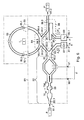
- an integrated-optical embodiment is diagrammatically shown of an S/C unit 81 for separating and combining an address signal and a data signal of a polarised packet signal, which corresponds to the S/C unit 23 of FIG. 2.
- the S/C unit 81 has a packet signal input 81.1 and a packet signal output 81.2.
- the S/C unit 81 comprises a polarisation controller 82, a mode splitter 83, a polarisation filter 84, a polarisation-maintaining delay line 85, a polarisation splitter used as combiner 86, a photodetector 87, and a laser 88 which is capable of being modulated.
- the polarisation controller 82 has a mono-modal input channel 82.1, which forms the packet signal input of the S/C unit 81, and a bi-modal output channel 82.2.
- the polarisation controller is of a kind as known from reference [9].
- the polarisation controller comprises a passive mode converter 89 for mode order number and polarisation (in this case, 100% TX 00 ⁇ TY 01 converter with TX is TE or TM, and TY is TM or TE).
- the polarisation controller further has two control signal inputs, 90 and 91 respectively, for a phase control signal and an amplitude control signal (control signal rr from FIG. 4).
- the polarisation controller is continuously controllable in such a manner that an optical signal, which enters via input channel 82.1 and is composed of two signal components with mutually orthogonal polarisations, appears in the output channel 82.2 as an optical signal in which the two signal components have the same polarisation but differ in order number (that is, as TY 00 and TY 01 signal).
- the mode splitter 83 is an asymmetric Y junction with a bi-modal stem 83.1 which forms the continuation of the bi-modal output channel 82.2 of the polarisation controller 82, a first mono-modal "wide" branch 83.2 which leads to the photodetector 87, and a mono-modal "narrow" branch 83.3.
- the polarisation filter is of a kind known from reference [10].
- Said filter is a TY filter, adapted to the chosen passive mode converter.
- the filter consists of two asymmetric Y junctions, each with a "narrow" mono-modal branch, 84.1 and 84.2 respectively, and a "wide” mono-modal branch, 84.3 and 84.4 respectively, which are coupled back-to-back via a common wave-guiding stem 84.5 which is mono-modal for the one polarisation (TX) and bi-modal for the other polarisation (TY).
- TX polarisation
- TY bi-modal for the other polarisation
- the “narrow" branch 83.3 of the mode splitter 83 is coupled via an adiabatic adapter to the "wide" branch 84.3 of the polarisation filter 84.
- the "wide” branch 84.4 is coupled to a first extremity 85.1 of the delay line 85, while the “narrow” branch 84.1 is coupled to the other extremity 85.2 of the delay line 85.
- the “narrow” branch 84.2 is coupled to a first mono-modal input channel 86.1 of the polarisation splitter 86, which is applied as combiner, while the laser 88 is connected to a second mono-modal input channel 86.2.
- a mono-modal output channel 86.3 of the polarisation splitter 86 forms the packet signal output of the S/C unit 81.
- the polarisation splitter shown here diagrammatically is of a kind as described in reference [11].
- the polarisation controller 82 In order to separate the address signal A 1 of a polarised packet signal P, which enters at the input 81.1 of the S/C unit 81, from the data signal I 0 and to be able to detect it via the photodetector 87, the polarisation controller 82 must be adjusted such that in the bi-modal output channel 82.2 the address signal is propagated as zero-order guided mode signal and the data signal as first-order guided mode signal. In that case, the address signal A 1 is conducted to the photodetector 87 via the "wide" branch 83.2 of the mode splitter 83, and is placed on the electrical output port 87.1 as electrical address signal A (for example, for a control unit 28 in FIG. 2).
- the data signal now as I 1 signal, propagates as zero-order TY mode via the "narrow" branch 83.1 of the mode splitter 83 and via the "wide” branches 84.3 and 84.4 of the polarisation filter to the input 85.1 of the delay line 85.
- the data signal I 1 After passing through the delay line 85 the data signal I 1 , still as zero-order TY mode, enters the polarisation filter 84 via the "narrow” branch 84.1 and leaves the filter in the same guided mode via the "narrow” branch 84.2.
- the data signal I 1 subsequently propagates unaltered through the polarisation splitter 86, via the input channel 86.1 and the output channel 86.3, to the packet signal output 81.2 of the S/C unit.
- the laser is modulated by an altered electrical address signal A' which is received at the electrical input port 88.1 of the laser 88 and sends an altered address signal A 0 ' to the input channel 86.2 of the polarisation splitter.
- the altered address signal A 0 ' is combined with the data signal I 1 into an outgoing polarised signal packet P' with an altered address signal.
- the delay line 85 can be coupled, directly or via mutually crossing wave-guides, with its extremities 85.1 and 85.2 to the 'narrow" branch 83.3 of the mode splitter 83 and the input channel 86.1 of the polarisation splitter 86.
- the mutually crossing wave-guides have the advantage of taking up less space.
- Such crossing wave-guides can be realised by channel-shaped wave-guides which intersect at a sufficiently large angle.
- a smaller embodiment is formed by two asymmetric Y junctions coupled by means of a common, bi-modal stem.
- the polarisation filter 84 again is a special form, in the sense that the common stem is bi-modal for one of the polarisations only. Thereby a signal is filtered in the signal passage via the "narrow" branches 84.1 and 84.2 to polarisation. This works correctively on the data signal I 1 in the case that the delay line 85 is not exactly polarisation-maintaining.
- the delay line 85 can be co-integrated, for example in the form of a spiralling loop. Since a signal propagating in TM mode in an integrated channel-shaped wave-guide experiences less damping, a TE 00 ⁇ TM 01 converter is preferably chosen for the passive mode converter 89 in the polarisation controller 82.
- a polarisation-maintaining fibre, of which the extremities 85.1 and 85.2 are connected, via suitable connectors 92 and 93 respectively, to the 'narrow" branch 84.1 and the "wide" branch 84.4 of the polarisation filter 84, can also be applied as delay line 85.
- Such an embodiment has the advantage that, for a specific application of the S/C unit 81, the delay period of the delay line can be simply adapted by means of a fibre of suitable length.
Landscapes
- Engineering & Computer Science (AREA)
- Computer Networks & Wireless Communication (AREA)
- Signal Processing (AREA)
- Optical Communication System (AREA)
- Data Exchanges In Wide-Area Networks (AREA)
- Use Of Switch Circuits For Exchanges And Methods Of Control Of Multiplex Exchanges (AREA)
Claims (10)
- Paketvermittlung zum Schalten von optischen Paketsignalen (P, Q), die mit einem Adressensignal (A1) und einem Datensignal (I0) versehen sind, die zueinander gemäss unterschiedlichen Polarisationszuständen polarisiert sind, wobei die besagte Vermittlung umfasst:dadurch gekennzeichnet, dass je Eingang der Vermittlungsmittel (7.1; ij) die Polarisation trennenden Mittel einen Polarisationsstrahlteiler (9; 29; 83) umfassen, der von einer Polarisationssteuerung (20; 36; 82) zum Steuern der relativen Polarisationsorientierung von einem einlaufenden Paketsignal in Bezug auf den Polarisationsstrahlteiler vorangegangen wird, wobei das Datensignal (I0; I1) und das Adressensignal (A1) jeweils an einem ersten (9.3; 29.2; 83.3) und einem zweiten (9.2; 29.3; 83.2) Ausgangsanschluss des Polarisationsstrahlteilers austreten.optische Vermittlungsmittel (7; 22), die mit einem oder mehreren Eingängen (7.1, 7.4; i1,...im) und zwei oder mehreren Ausgängen (7.2, 7.3; u1,...un) versehen sind, die so angeordnet sind, um jeweils mit einlaufenden und ausgehenden optischen Übertragungsleitungen verbunden zu werden,Polarisationen trennende Mittel (8, 9, 10, 20; 29, 30, 36; 82, 83) zum Trennen von Adressensignalen von den Paketsignalen, die über die einlaufenden Übertragungsleitungen eintreten, undSteuermittel (11; 28) zum Ableiten von Steuersignalen (c; cc) von den getrennten Adressensignalen (A1) zum Steuern des Weiterleitens der Paketsignale durch die Vermittlungsmittel von dem Eingang, an dem ein betreffendes Paketsignal eingegangen ist, an den Ausgang des Vermittlungsmittels, der von dem getrennten Adressensignal (A1) des betreffenden Paketsignals abgeleitet worden ist,
- Paketvermittlung nach Anspruch 1, dadurch gekennzeichnet, dass die Steuermittel (28) mit Adressenmodifikationsmitteln zum Erzeugen, in Antwort auf ein eingetroffenes Paketsignal, eines modifizierten optischen Adressensignals (A'1; A'0), welches im wesentlichen dieselbe Wellenlänge wie das getrennte Adressensignal (A1) hat, und dass je Eingang die Paketvermittlung weiterhin ein Polarisationstrahl kombinierendes Mittel (32; 86) umfasst zum Kombinieren des modifizierten optischen Adressensignals und des Datensignals (I0; I1), das an dem ersten Ausgangsanschluss (29,1: 83.3) des Polarisationsstrahlteilers (29; 83) austritt, in ein polarisiertes Paket (P'), wobei das besagte Polarisationstrahl kombinierende Mittel mit einem ersten Eingangsanschluss (32.1; 86.1), der mit dem ersten Ausgangsanschluss (29.2; 83.3) des betreffenden Polarisationsstrahlteilers verbunden ist, mit einem zweiten Eingangsanschluss (32.2; 86.2), der mit den Adressenmodifikationsmitteln verbunden ist, und mit einem Ausgangsanschluss (32.3; 86.3) versehen ist, der mit einem Eingang (ij) der Vermittlungsmittel (22) verbunden ist.
- Paketvermittlung nach Anspruch 2, dadurch gekennzeichnet, dass der erste Eingangsanschluss (32.1; 86.1) des Polarisationsstrahlkombinierers (32; 86) und der erste Ausgangsanschluss (29.2; 83.3) des Polarisationsstrahlteilers (29; 83) über einen die Polarisation erhaltenden Wellenleiter (33; 85) verbunden sind.
- Paketvermittlung nach Anspruch 3, dadurch gekennzeichnet, dass die Polarisationssteuerung auf einem passiven Modenwandler (89) basiert, um einen geführten Mode nullter Ordnung einer ersten Polarisation in einen geführten Mode erster Ordnung einer zweiten Polarisation zu wandeln, die senkrecht zur ersten Polarisation steht, und die mit einem monomodalen Eingangskanal (82.1) und einem bimodalen Ausgangskanal (82.2) versehen ist, dass der Polarisationsstrahlteiler (83) ein Modenteiler ist, der auf einer asymmetrischen Y-Verzweigung mit einem bimodalen Stamm (83.1) basiert, der mit dem bimodalen Ausgangskanal der Polarisationssteuerung verbunden ist.
- Paketvermittlung nach Anspruch 3 oder Anspruch 4, dadurch gekennzeichnet, dass die Paketvermittlung weiterhin einen optischen Verzögerungsweg (85) umfasst, der in dem Polarisation aufrechterhaltenden Wellenleiter über eine Wellenleiterkreuzung (84) eingeschlossen ist.
- Paketvermittlung nach Anspruch 5, dadurch gekennzeichnet, dass die Wellenleiterkreuzung durch einen Polarisationsfilter (84) ausgebildet ist.
- Paketvermittlung nach Anspruch 1, dadurch gekennzeichnet, dass je Eingang der Vermittlungsmittel weiterhin ein Leistungsteiler (8) vorgesehen ist, der mit einem Eingangsanschluss (8.1), der so angeordnet ist, um mit einem Ende einer betreffenden Übertragungsleitung (4) verbunden zu werden, und mit einem ersten Ausgangsanschluss (8.2) versehen ist, der mit einem betreffenden Eingang (7.1) der Vermittlungsmittel (7) verbunden ist, und für einen zweiten Ausgangsanschluss (8.3), der mit einem Eingangsanschluss der Polarisationssteuerung (20) verbunden ist.
- Optisches paketvermitteltes Netzwerk mit einer Anzahl von Knoten, die über optische Verbindungen verbunden sind, in welchem Netzwerk ein erster Knoten der Anzahl von Knoten mit einem Übertragungsmittel (6) versehen ist, um optische Paketsignale (P) zu erzeugen und über die optische Verbindung zu übertragen, in dem jedes Paketsignal ein Adressensignal (A1) und ein Datensignal (I0) umfasst, die gemäss zueinander verschiedenen Polarisationszuständen polarisiert sind, dadurch gekennzeichnet, dass ein zweiter Knoten der Anzahl der Knoten mit einer Paketvermittlung gemäss einem der Ansprüche 1 bis 7 versehen ist.
- Optisches paketvermitteltes Netzwerk gemäss Anspruch 8, dadurch gekennzeichnet, dass die Übertragungsmittel Steuermittel (43; 62), einen optischen Signalgenerator (41, 42; 61), der so angeordnet ist, um durch die Steuermittel moduliert zu werden und um über einen ausgehenden optischen Wellenleiter ein Paketsignal zu übertragen, das gemäss der Paketstruktur moduliert ist, und die Polarisation setzende Mittel (41, 42, 44; 63) umfassen, die durch die Steuermittel schaltbar sind, die in dem ausgehenden optischen Wellenleiter umfasst sind, für das vermittlungsweise Setzen unter der Steuerung der Steuermittel der Polarisation des Adressensignals gemäss einem ersten Polarisationszustand und des Datensignals gemäss einem zweiten Polarisationszustand, der sich von dem ersten Polarisationszustand unterscheidet, für jedes Paketsignal, das über den ausgehenden Wellenleiter übertragen wird.
- Optisches paketvermitteltes Netzwerk gemäss Anspruch 9, dadurch gekennzeichnet, dass der ausgehende Wellenleiter ein monomodaler wellenleitender Kanal, in dem sich ein Paketsignal gemäss einem Mode nullter Ordnung einer ersten Polarisation von zwei zueinander orthogonalen Polarisationen (TE, TM) ausbreitet, und dass das vermittelbare die Polarisation setzende Mittel in einer Reihenschaltung einen schaltbaren (66) und einen passiven (67) Polarisationswandler umfassen, dass der besagte schaltbare Polarisationswandler zwischen einem ersten Schaltzustand, in dem ein Mode nullter Ordnung der ersten Polarisation (TE oder TM) in einen Mode erster Ordnung der zweiten Polarisation (TM oder TE) gewandelt wird, und einem zweiten Schaltzustand schaltbar ist, in dem keine Wandlung stattfindet, wobei der besagte passive Polarisationswandler einen Mode erster Ordnung der zweiten Polarisation (TM oder TE) in einen Mode nullter Ordnung der zweiten Polarisation wandelt.
Applications Claiming Priority (4)
| Application Number | Priority Date | Filing Date | Title |
|---|---|---|---|
| NL1002544A NL1002544C2 (nl) | 1996-03-06 | 1996-03-06 | Optisch pakket-geschakeld systeem. |
| NL1002544 | 1996-03-06 | ||
| NL1005263A NL1005263C2 (nl) | 1996-03-06 | 1997-02-12 | Optisch pakket-geschakeld transmissie-netwerk. |
| NL1005263 | 1997-02-12 |
Publications (2)
| Publication Number | Publication Date |
|---|---|
| EP0794684A1 EP0794684A1 (de) | 1997-09-10 |
| EP0794684B1 true EP0794684B1 (de) | 2005-03-23 |
Family
ID=26642342
Family Applications (1)
| Application Number | Title | Priority Date | Filing Date |
|---|---|---|---|
| EP97200571A Expired - Lifetime EP0794684B1 (de) | 1996-03-06 | 1997-02-27 | Optisches Paketvermittlungssystem |
Country Status (5)
| Country | Link |
|---|---|
| US (1) | US5900957A (de) |
| EP (1) | EP0794684B1 (de) |
| AT (1) | ATE291823T1 (de) |
| DE (1) | DE69732814T2 (de) |
| NL (1) | NL1005263C2 (de) |
Families Citing this family (30)
| Publication number | Priority date | Publication date | Assignee | Title |
|---|---|---|---|---|
| CN1270732A (zh) * | 1997-09-17 | 2000-10-18 | 英国电讯有限公司 | 计算机 |
| US6292598B1 (en) * | 1998-11-04 | 2001-09-18 | Corvis Corporation | Optical transmission apparatuses, methods, and systems |
| US6118566A (en) * | 1998-11-04 | 2000-09-12 | Corvis Corporation | Optical upconverter apparatuses, methods, and systems |
| KR100341394B1 (ko) * | 1999-12-03 | 2002-06-22 | 오길록 | 광 패킷 스위치의 광 패킷 헤더 처리장치 |
| JP3374174B2 (ja) * | 1999-12-15 | 2003-02-04 | 独立行政法人通信総合研究所 | フォトニックネットワークのパケットルーティング方法およびフォトニックネットワーク用パケットルータ |
| US6626589B1 (en) * | 1999-12-29 | 2003-09-30 | Nortel Networks Limited | Optical packet switching |
| JP3578960B2 (ja) * | 2000-02-28 | 2004-10-20 | 日本電信電話株式会社 | 超高速光パケット転送リングネットワーク、光挿入分岐型多重分離ノード装置及び光挿入分岐型多重分離ノード装置の動作方法 |
| US6426831B1 (en) | 2000-02-29 | 2002-07-30 | Massachusetts Institute Of Technology | EIT based optical switch/wavelength converter |
| FI20000670L (fi) | 2000-03-22 | 2001-09-23 | Nokia Networks Oy | Optinen pakettikytkin |
| EP1202485A1 (de) * | 2000-10-18 | 2002-05-02 | Alcatel | Verfahren zum Übertragen eines optischen Multiplexsignals sowie Sender und Empfänger dafür |
| CA2428230A1 (en) * | 2000-11-08 | 2002-05-16 | Yaron Mayer | System and method for improving network router efficiency and alleviating network bottlenecks and overloads |
| US20030128987A1 (en) * | 2000-11-08 | 2003-07-10 | Yaron Mayer | System and method for improving the efficiency of routers on the internet and/or cellular networks an/or other networks and alleviating bottlenecks and overloads on the network |
| US6594050B2 (en) * | 2001-01-03 | 2003-07-15 | Physical Optics Corporation | Optical communication switch node |
| FR2822304A1 (fr) * | 2001-03-16 | 2002-09-20 | Teem Photonics | Structure d'amplification optique realisee en optique integree et boitier d'amplification integrant une telle structure |
| DE60126842T2 (de) * | 2001-08-16 | 2007-08-30 | Telefonaktiebolaget Lm Ericsson (Publ) | Optischer verstärker |
| US7106967B2 (en) * | 2001-09-04 | 2006-09-12 | Doron Handelman | Optical packet switching apparatus and methods |
| AU2002366987A1 (en) * | 2001-12-28 | 2003-07-30 | Al Baur | System and method for improving network router efficiency and alleviating network bottlenecks and overloads |
| US6904189B2 (en) * | 2002-02-22 | 2005-06-07 | Lynx Photonic Networks, Inc. | Fast wavelength-selective switch elements and switch matrices |
| US7280764B2 (en) * | 2002-03-01 | 2007-10-09 | Avago Technologies Fiber Ip (Singapore) Pte Ltd | Optical signal multiplexer/demultiplexer employing pseudorandom mode modulation |
| US7130539B2 (en) * | 2002-08-22 | 2006-10-31 | Main Street Ventures, Llc | All optical decoding systems for optical encoded data symbols |
| US7007208B1 (en) * | 2002-05-31 | 2006-02-28 | Finisar Corporation | Systems and methods for data unit modification |
| US20040109445A1 (en) * | 2002-12-09 | 2004-06-10 | Julie Fouquet | Systems and methods for selectively diverting data from nodes |
| NO320962B1 (no) * | 2003-07-04 | 2006-02-20 | Telenor Asa | Anvendelse av polarisasjon for a skille ulike typer informasjon |
| KR100602269B1 (ko) * | 2004-11-02 | 2006-07-19 | 삼성전자주식회사 | 파장 오프셋 편광분할 다중화 방식의 레이블링을 이용한광 패킷 통신 시스템 |
| EP2119074A1 (de) | 2007-03-15 | 2009-11-18 | Telefonaktiebolaget LM Ericsson (PUBL) | Kommunikationsknoten und verfahren zum routen von optischen datenpaketsignalen |
| EP2109233B1 (de) * | 2008-04-11 | 2010-08-04 | Alcatel Lucent | Modulationsschema mit erhöhter Anzahl Polarisierungszustände |
| JP2011188213A (ja) * | 2010-03-08 | 2011-09-22 | Fujitsu Ltd | 光信号送信装置、光増幅装置、光減衰装置及び光信号送信方法 |
| GB201101709D0 (en) * | 2011-02-01 | 2011-03-16 | Transpacket As | A method and a node arrangement for optimizing traffic processing in integrated hybrid networks |
| US8995049B2 (en) * | 2011-09-08 | 2015-03-31 | Northrop Grumman Systems Corporation | Method and apparatus for suppression of stimulated brillouin scattering using polarization control with a birefringent delay element |
| US10015568B2 (en) * | 2016-10-11 | 2018-07-03 | Fluke Corporation | Optically-addressable optical switch |
Family Cites Families (7)
| Publication number | Priority date | Publication date | Assignee | Title |
|---|---|---|---|---|
| JPH0834479B2 (ja) * | 1987-10-22 | 1996-03-29 | 国際電信電話株式会社 | 光パケット交換方式 |
| NL9100852A (nl) * | 1991-05-16 | 1992-12-16 | Nederland Ptt | Modusomzetter. |
| NL9101226A (nl) * | 1991-07-11 | 1993-02-01 | Nederland Ptt | Polarisatiefilter. |
| NL9200328A (nl) * | 1992-02-21 | 1993-09-16 | Nederland Ptt | Optische schakelcomponent. |
| NL9200576A (nl) * | 1992-03-27 | 1993-10-18 | Nederland Ptt | Regelbare polarisatie-omvormer. |
| SG48849A1 (en) * | 1992-04-09 | 1998-05-18 | British Telecomm | Optical processing system |
| NL1000182C2 (nl) * | 1995-04-20 | 1996-10-22 | Nederland Ptt | Geïntegreerde optische polarisatie-splitser. |
-
1997
- 1997-02-12 NL NL1005263A patent/NL1005263C2/nl not_active IP Right Cessation
- 1997-02-27 DE DE69732814T patent/DE69732814T2/de not_active Expired - Lifetime
- 1997-02-27 EP EP97200571A patent/EP0794684B1/de not_active Expired - Lifetime
- 1997-02-27 AT AT97200571T patent/ATE291823T1/de not_active IP Right Cessation
- 1997-02-28 US US08/808,310 patent/US5900957A/en not_active Expired - Fee Related
Also Published As
| Publication number | Publication date |
|---|---|
| DE69732814D1 (de) | 2005-04-28 |
| NL1005263C2 (nl) | 1997-09-09 |
| US5900957A (en) | 1999-05-04 |
| ATE291823T1 (de) | 2005-04-15 |
| EP0794684A1 (de) | 1997-09-10 |
| DE69732814T2 (de) | 2006-05-11 |
Similar Documents
| Publication | Publication Date | Title |
|---|---|---|
| EP0794684B1 (de) | Optisches Paketvermittlungssystem | |
| AU669699B2 (en) | Optical processing system | |
| US5319486A (en) | Transmission equipment with an optical transmission line | |
| US5548431A (en) | Bidirectional multi-channel optical ring network using WDM techniques | |
| US5600466A (en) | Wavelength division optical signalling network apparatus and method | |
| KR910003238B1 (ko) | 광 통신 시스템 및 이 시스템의 중앙지국과 원격지국 | |
| US5317658A (en) | Apparatus and method for providing a polarization independent optical switch | |
| EP0347903A3 (de) | Schnelles optisches Paketvermittlungssystem mit optischen Puffern zwischen ankommenden und abgehenden Kanälen | |
| US4815803A (en) | Optical signal network with node by-pass switching capability | |
| EP0189273A2 (de) | Lichtwellenleiternetzwerk mit verminderten Kopplungsverlusten | |
| US6594049B1 (en) | Optical router | |
| Jonsson | Optical interconnection technology in switches, routers and optical cross connects | |
| NL1002544C2 (nl) | Optisch pakket-geschakeld systeem. | |
| JP2725704B2 (ja) | 情報信号と制御信号の光伝送方法 | |
| US6542269B1 (en) | Optical device for processing an optical impulse | |
| US6577425B1 (en) | Optical device for processing a sequence of bits | |
| JP2976667B2 (ja) | ループ型光ローカルエリアネットワークシステムにおけるアクセス制御方式およびそのノード装置 | |
| JPH01108530A (ja) | 光駆動形スイッチ | |
| JP3003207B2 (ja) | 光ローカルエリアネットワークシステムのアクセス制御方式及びノード装置 | |
| Glance et al. | Large capacity multiaccess optical packet network | |
| Goodman et al. | Demonstration of fast wavelength tuning for a high performance packet switch | |
| KR950009420B1 (ko) | 광 링 통신망 구성방법 | |
| AU762271B2 (en) | Optical device for processing a sequence of bits | |
| US20020075541A1 (en) | System, device, and method for producing optical data streams in an optical communication network | |
| US8553326B2 (en) | Add and drop circulator |
Legal Events
| Date | Code | Title | Description |
|---|---|---|---|
| PUAI | Public reference made under article 153(3) epc to a published international application that has entered the european phase |
Free format text: ORIGINAL CODE: 0009012 |
|
| AK | Designated contracting states |
Kind code of ref document: A1 Designated state(s): AT BE CH DE DK ES FI FR GB GR IE IT LI LU NL PT SE |
|
| 17P | Request for examination filed |
Effective date: 19980310 |
|
| RAP3 | Party data changed (applicant data changed or rights of an application transferred) |
Owner name: KONINKLIJKE KPN N.V. |
|
| 17Q | First examination report despatched |
Effective date: 20040127 |
|
| GRAP | Despatch of communication of intention to grant a patent |
Free format text: ORIGINAL CODE: EPIDOSNIGR1 |
|
| RIN1 | Information on inventor provided before grant (corrected) |
Inventor name: VAN DER TOL, JOHANNES JACOBUS GERARDUS MARIA |
|
| GRAS | Grant fee paid |
Free format text: ORIGINAL CODE: EPIDOSNIGR3 |
|
| GRAA | (expected) grant |
Free format text: ORIGINAL CODE: 0009210 |
|
| AK | Designated contracting states |
Kind code of ref document: B1 Designated state(s): AT BE CH DE DK ES FI FR GB GR IE IT LI LU NL PT SE |
|
| PG25 | Lapsed in a contracting state [announced via postgrant information from national office to epo] |
Ref country code: NL Free format text: LAPSE BECAUSE OF FAILURE TO SUBMIT A TRANSLATION OF THE DESCRIPTION OR TO PAY THE FEE WITHIN THE PRESCRIBED TIME-LIMIT Effective date: 20050323 Ref country code: IT Free format text: LAPSE BECAUSE OF FAILURE TO SUBMIT A TRANSLATION OF THE DESCRIPTION OR TO PAY THE FEE WITHIN THE PRESCRIBED TIME-LIMIT;WARNING: LAPSES OF ITALIAN PATENTS WITH EFFECTIVE DATE BEFORE 2007 MAY HAVE OCCURRED AT ANY TIME BEFORE 2007. THE CORRECT EFFECTIVE DATE MAY BE DIFFERENT FROM THE ONE RECORDED. Effective date: 20050323 Ref country code: FI Free format text: LAPSE BECAUSE OF FAILURE TO SUBMIT A TRANSLATION OF THE DESCRIPTION OR TO PAY THE FEE WITHIN THE PRESCRIBED TIME-LIMIT Effective date: 20050323 Ref country code: BE Free format text: LAPSE BECAUSE OF FAILURE TO SUBMIT A TRANSLATION OF THE DESCRIPTION OR TO PAY THE FEE WITHIN THE PRESCRIBED TIME-LIMIT Effective date: 20050323 Ref country code: AT Free format text: LAPSE BECAUSE OF FAILURE TO SUBMIT A TRANSLATION OF THE DESCRIPTION OR TO PAY THE FEE WITHIN THE PRESCRIBED TIME-LIMIT Effective date: 20050323 |
|
| REG | Reference to a national code |
Ref country code: GB Ref legal event code: FG4D |
|
| REG | Reference to a national code |
Ref country code: CH Ref legal event code: NV Representative=s name: ISLER & PEDRAZZINI AG Ref country code: CH Ref legal event code: EP |
|
| REG | Reference to a national code |
Ref country code: IE Ref legal event code: FG4D |
|
| REF | Corresponds to: |
Ref document number: 69732814 Country of ref document: DE Date of ref document: 20050428 Kind code of ref document: P |
|
| PG25 | Lapsed in a contracting state [announced via postgrant information from national office to epo] |
Ref country code: GR Free format text: LAPSE BECAUSE OF FAILURE TO SUBMIT A TRANSLATION OF THE DESCRIPTION OR TO PAY THE FEE WITHIN THE PRESCRIBED TIME-LIMIT Effective date: 20050623 Ref country code: DK Free format text: LAPSE BECAUSE OF FAILURE TO SUBMIT A TRANSLATION OF THE DESCRIPTION OR TO PAY THE FEE WITHIN THE PRESCRIBED TIME-LIMIT Effective date: 20050623 |
|
| PG25 | Lapsed in a contracting state [announced via postgrant information from national office to epo] |
Ref country code: ES Free format text: LAPSE BECAUSE OF FAILURE TO SUBMIT A TRANSLATION OF THE DESCRIPTION OR TO PAY THE FEE WITHIN THE PRESCRIBED TIME-LIMIT Effective date: 20050704 |
|
| NLV1 | Nl: lapsed or annulled due to failure to fulfill the requirements of art. 29p and 29m of the patents act | ||
| PG25 | Lapsed in a contracting state [announced via postgrant information from national office to epo] |
Ref country code: PT Free format text: LAPSE BECAUSE OF FAILURE TO SUBMIT A TRANSLATION OF THE DESCRIPTION OR TO PAY THE FEE WITHIN THE PRESCRIBED TIME-LIMIT Effective date: 20050907 |
|
| PLBE | No opposition filed within time limit |
Free format text: ORIGINAL CODE: 0009261 |
|
| STAA | Information on the status of an ep patent application or granted ep patent |
Free format text: STATUS: NO OPPOSITION FILED WITHIN TIME LIMIT |
|
| ET | Fr: translation filed | ||
| PG25 | Lapsed in a contracting state [announced via postgrant information from national office to epo] |
Ref country code: IE Free format text: LAPSE BECAUSE OF NON-PAYMENT OF DUE FEES Effective date: 20060227 |
|
| PG25 | Lapsed in a contracting state [announced via postgrant information from national office to epo] |
Ref country code: LU Free format text: LAPSE BECAUSE OF NON-PAYMENT OF DUE FEES Effective date: 20060228 |
|
| 26N | No opposition filed |
Effective date: 20051227 |
|
| REG | Reference to a national code |
Ref country code: IE Ref legal event code: MM4A |
|
| REG | Reference to a national code |
Ref country code: CH Ref legal event code: PCAR Free format text: ISLER & PEDRAZZINI AG;POSTFACH 1772;8027 ZUERICH (CH) |
|
| PG25 | Lapsed in a contracting state [announced via postgrant information from national office to epo] |
Ref country code: SE Free format text: LAPSE BECAUSE OF FAILURE TO SUBMIT A TRANSLATION OF THE DESCRIPTION OR TO PAY THE FEE WITHIN THE PRESCRIBED TIME-LIMIT Effective date: 20050623 |
|
| REG | Reference to a national code |
Ref country code: CH Ref legal event code: PUE Owner name: AMSTR. INVESTMENTS 23 K.G., LLC Free format text: KONINKLIJKE KPN N.V.#STATIONSPLEIN 7#9726 AE GRONINGEN (NL) -TRANSFER TO- AMSTR. INVESTMENTS 23 K.G., LLC#2711 CENTERVILLE RD., SUITE 400#WILMINGTON DE 19808 (US) |
|
| PGFP | Annual fee paid to national office [announced via postgrant information from national office to epo] |
Ref country code: CH Payment date: 20100223 Year of fee payment: 14 |
|
| REG | Reference to a national code |
Ref country code: FR Ref legal event code: TP |
|
| REG | Reference to a national code |
Ref country code: GB Ref legal event code: 732E Free format text: REGISTERED BETWEEN 20100617 AND 20100623 |
|
| REG | Reference to a national code |
Ref country code: CH Ref legal event code: PL |
|
| PG25 | Lapsed in a contracting state [announced via postgrant information from national office to epo] |
Ref country code: LI Free format text: LAPSE BECAUSE OF NON-PAYMENT OF DUE FEES Effective date: 20110228 Ref country code: CH Free format text: LAPSE BECAUSE OF NON-PAYMENT OF DUE FEES Effective date: 20110228 |
|
| REG | Reference to a national code |
Ref country code: FR Ref legal event code: PLFP Year of fee payment: 20 |
|
| PGFP | Annual fee paid to national office [announced via postgrant information from national office to epo] |
Ref country code: DE Payment date: 20160302 Year of fee payment: 20 |
|
| PGFP | Annual fee paid to national office [announced via postgrant information from national office to epo] |
Ref country code: GB Payment date: 20160127 Year of fee payment: 20 Ref country code: FR Payment date: 20160125 Year of fee payment: 20 |
|
| REG | Reference to a national code |
Ref country code: DE Ref legal event code: R071 Ref document number: 69732814 Country of ref document: DE |
|
| REG | Reference to a national code |
Ref country code: GB Ref legal event code: PE20 Expiry date: 20170226 |
|
| PG25 | Lapsed in a contracting state [announced via postgrant information from national office to epo] |
Ref country code: GB Free format text: LAPSE BECAUSE OF EXPIRATION OF PROTECTION Effective date: 20170226 |
|
| REG | Reference to a national code |
Ref country code: DE Ref legal event code: R082 Ref document number: 69732814 Country of ref document: DE Representative=s name: SCHOEN, THILO, DIPL.-PHYS., DE |