EP0792464B1 - Messanordnung für einen koaxialleiter zur bestimmung des energiedurchflusses und des welligkeitsverhältnisses - Google Patents
Messanordnung für einen koaxialleiter zur bestimmung des energiedurchflusses und des welligkeitsverhältnisses Download PDFInfo
- Publication number
- EP0792464B1 EP0792464B1 EP95937291A EP95937291A EP0792464B1 EP 0792464 B1 EP0792464 B1 EP 0792464B1 EP 95937291 A EP95937291 A EP 95937291A EP 95937291 A EP95937291 A EP 95937291A EP 0792464 B1 EP0792464 B1 EP 0792464B1
- Authority
- EP
- European Patent Office
- Prior art keywords
- impedance
- conductor
- directional coupler
- microstrip
- output
- Prior art date
- Legal status (The legal status is an assumption and is not a legal conclusion. Google has not performed a legal analysis and makes no representation as to the accuracy of the status listed.)
- Expired - Lifetime
Links
- 239000004020 conductor Substances 0.000 title claims description 64
- 238000005259 measurement Methods 0.000 claims description 5
- 238000000034 method Methods 0.000 claims description 4
- 230000001808 coupling effect Effects 0.000 claims description 3
- 238000004519 manufacturing process Methods 0.000 description 3
- 230000005540 biological transmission Effects 0.000 description 2
- 239000002131 composite material Substances 0.000 description 2
- 238000010276 construction Methods 0.000 description 2
- 238000005516 engineering process Methods 0.000 description 2
- 238000011156 evaluation Methods 0.000 description 2
- 239000000523 sample Substances 0.000 description 2
- ATJFFYVFTNAWJD-UHFFFAOYSA-N Tin Chemical compound [Sn] ATJFFYVFTNAWJD-UHFFFAOYSA-N 0.000 description 1
- 230000006978 adaptation Effects 0.000 description 1
- 238000004458 analytical method Methods 0.000 description 1
- 230000009286 beneficial effect Effects 0.000 description 1
- 230000008878 coupling Effects 0.000 description 1
- 238000010168 coupling process Methods 0.000 description 1
- 238000005859 coupling reaction Methods 0.000 description 1
- 230000001419 dependent effect Effects 0.000 description 1
- 238000001514 detection method Methods 0.000 description 1
- 238000010586 diagram Methods 0.000 description 1
- 239000003989 dielectric material Substances 0.000 description 1
- 230000000694 effects Effects 0.000 description 1
- 230000005669 field effect Effects 0.000 description 1
- 230000001771 impaired effect Effects 0.000 description 1
- 239000002184 metal Substances 0.000 description 1
- 238000010606 normalization Methods 0.000 description 1
- IHQKEDIOMGYHEB-UHFFFAOYSA-M sodium dimethylarsinate Chemical class [Na+].C[As](C)([O-])=O IHQKEDIOMGYHEB-UHFFFAOYSA-M 0.000 description 1
- 229910000679 solder Inorganic materials 0.000 description 1
- 238000005476 soldering Methods 0.000 description 1
- 238000011144 upstream manufacturing Methods 0.000 description 1
Images




Classifications
-
- G—PHYSICS
- G01—MEASURING; TESTING
- G01R—MEASURING ELECTRIC VARIABLES; MEASURING MAGNETIC VARIABLES
- G01R27/00—Arrangements for measuring resistance, reactance, impedance, or electric characteristics derived therefrom
- G01R27/02—Measuring real or complex resistance, reactance, impedance, or other two-pole characteristics derived therefrom, e.g. time constant
- G01R27/04—Measuring real or complex resistance, reactance, impedance, or other two-pole characteristics derived therefrom, e.g. time constant in circuits having distributed constants, e.g. having very long conductors or involving high frequencies
- G01R27/06—Measuring reflection coefficients; Measuring standing-wave ratio
-
- G—PHYSICS
- G01—MEASURING; TESTING
- G01R—MEASURING ELECTRIC VARIABLES; MEASURING MAGNETIC VARIABLES
- G01R1/00—Details of instruments or arrangements of the types included in groups G01R5/00 - G01R13/00 and G01R31/00
- G01R1/20—Modifications of basic electric elements for use in electric measuring instruments; Structural combinations of such elements with such instruments
- G01R1/24—Transmission-line, e.g. waveguide, measuring sections, e.g. slotted section
Definitions
- the present invention relates to a measuring line, or test line, that can be coupled to a coaxial conductor. More specifically, the invention relates to a measuring line, or test line, of the kind defined in the preamble of present Claim 1.
- Such measuring lines are often used in connection with antenna-connected conductors, e.g. in mobile telephony systems, intended for the UHF range.
- the transmitted energy is often comprised of several different carrier waves which have a mutual radio-channel spacing and which are intended for transmission on one and the same antenna, and consequently measuring of the composite power is of interest, despite being able to measure the transmission power of each modulated carrier wave per se.
- the standing-wave ratio is measured and monitored for the composite power, so as to be able to check antenna function among other things, since faults in an antenna function will normally result in mismatching noticeable by reflections, this mismatching immediately having a marked effect on the standing-wave ratio.
- Measuring lines of the kind defined in the introduction and capable of being connected to a coaxial conductor or line with the aid of conventional coaxial contacts are known to the art, wherein the microwave energy is conducted through a hollow conductor which includes an inner conductor that is connected to the centre conductor of the coaxial connections and which has overall the same impedance as the coaxial conductor, e.g. an impedance of 50 ohms.
- a typical type is the so-called slab line, which is a type of TEM conductor and consists of a centre conductor placed between two parallel surfaces which together with narrower side surfaces and end surfaces define a flat, box-like configuration.
- slab line which is a type of TEM conductor and consists of a centre conductor placed between two parallel surfaces which together with narrower side surfaces and end surfaces define a flat, box-like configuration.
- a directional coupler is located on each of said sides. The directional couplers are earthed at respective opposite ends via a matching resistor, whereas the non-earthed ends are each coupled to a respective measuring device, whereby the ratio between the output powers each representing a respective propagation direction can be measured and the standing-wave ratio can be calculated in voltage measurements (VSWR).
- One object of the present invention is to provide a measuring device of the aforesaid kind which can be produced more cheaply and more simply.
- Another object of the invention is to provide in said device room for a measuring probe, a so-called test coupler.
- the aforesaid objects and advantages afforded by the invention are achieved by arranging in the hollow conductor solely one single directional coupler conductor which has symmetrically disposed transverse branch lines which are drawn through openings in a wall of the hollow conductor and each of which extends to a respective adapted conductor in a circuit board mounted externally of said wall, wherein the directional coupler conductor within the cavity and the lines or conductors on the circuit board have mutually matched impedances.
- circuit board technology it is therewith possible to achieve the necessary precision much more cheaply and much more simply than can be achieved with conventional workshop practice.
- the directional coupler conductor will preferably have a higher impedance than that of the hollow conductor, wherein an upper limit is set for reasons of mechanical stability because a high impedance means a narrow or slender directional coupler conductor and because a narrow directional coupler is unable to cope without the support of a dielectric material, which would result in impaired directivity.
- the length of the directional coupler is contingent on the wavelength used and will preferably be about one-quarter of a wavelength.
- the directional coupler will preferably have an impedance of 60-90 ⁇ , and preferably an impedance of about 75 ⁇ .
- An attenuating circuit is preferably also placed immediately after the hollow conductor outlet.
- the directional coupler has a coupling effect of 35-55 dB and with an attenuation of 10-20 dB in a well-adapted attenuation circuit, the reflection from following essentially matched but not necessarily fully linear measuring circuits will be so negligible that the intermodulation phenomenon on the signals transmitted in the hollow conductor will become negligibly small.
- a particular advantage afforded by the invention is therefore that as large a part as possible of the termination sensed by the ends of the directional coupler is placed in a circuit board, said construction enabling reproducible and inexpensive series manufacture, in the preferred embodiment using microstrip technology. Strip line techniques and similar techniques may also be used.
- the output signal is thereafter conveniently amplified prior to being passed to a voltage-controlled attenuation circuit upstream of a detector diode, the detector signal of which is amplified and passed through a lowpass filter that has a relatively long time constant (e.g. 0.2-2 s.), wherein the filtered signal is fed back to the voltage-controlled attenuation circuit and constitutes a measurement of the captured power in a logarithmic scale.
- One of these ends will deliver a signal corresponding to the forwardly directed power in the measuring line, while the other end will produce a signal corresponding to the reflected power.
- each of these power signals is passed to a respective A/D converter and is there forwarded to a calculating circuit, which may include alarm outputs, which are activated upon the occurrence of excessively high standing-wave ratios, indicating instruments, etc. It is beneficial to mount these process circuits on a circuit board in one and the same unit, for instance on the opposite side of the hollow conductor in relation to the circuit board to which the directional coupler is connected.
- Fig. 1 illustrates an opened measuring line, including a box 1 which at the short ends has two coaxial contacts 2 whose central conductors are joined to a centre conductor 3 which forms in the enclosed cavity together with the broad sides of the box a slab line which is adapted to the coaxial conductors (not shown) to be connected.
- the centre conductor may have a diameter of 5 mm and the distance between the broad walls may be 9 mm.
- a symmetric directional coupler 4 is spaced above the nearest broad wall at a side distance of 14 mm therefrom, said coupler having the form of a rod of 3 mm in diameter meaning an impedance of 75 ⁇ and a coupling effect of roughly -38 dB.
- a test line 5 is mounted on the opposite side of the central conductor and has a matching resistor 7 connected directly to the broad wall and includes a through-extending coaxial contact 6 for connection to a measuring circuit.
- Fig. 2 shows one terminal connection of the directional coupler 4 connected to an external circuit board 10 through the medium of a short carrier cylinder 8 extending through a hole 9 in the wall.
- the illustrated circuit board includes a microstrip, as described below. Only a very short length of the carrier cylinder 8 is less well adapted or matched, due to the fact that the diameter of the hole 9 is adapted to the diameter of the cylinder 8.
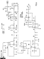
- Fig. 4 illustrates components used on the circuit board 10 (Fig. 2), it may be appropriate to read Figs. 3 and 4 together.
- energy is conducted from respective ends of the directional coupler 4 to a circuit board that has a first attenuation circuit as well as an impedance transformer 30 with an attenuation of 15 dB, followed by a second attenuator 31 which although marked as being adjustable is in practice set in manufacture by appropriate component selection to achieve normalization and compensation of manufacturing tolerances.
- amplifiers 32, 34 which are separated by an attenuator to prevent self-oscillation.
- the thus amplified power signal is now conducted to a voltage-controlled attenuator 35 (AT-109 from M/A-COM, Lowell, U.S.A.).
- This component is based on field effect transistors and is able to attenuate frequencies of between 0.5 and 2 GHz by between 0 and -35 dB and is generally linear, expressed in dB/V.
- detector diode 36 with associated filter.
- a similar diode 37 is provided by the side of the diode 36 and is supplied with direct current as like as is possible, which results in a reference voltage Fwd ref, and the two voltages are each delivered to a respective input on differential amplifier 38, thereby obtaining temperature compensation for the detection.
- the temperature compensated signal thus obtained is passed to further amplifiers 40 and 41 via a lowpass filter and the output signal Vfwd is fed back to the voltage-controlled attenuator 35.
- the diode D1 (Fig. 4) prevents the control voltage of the voltage-controlled attenuator from becoming higher than its supply voltage and therefore protects the attenuator.
- the output voltage will now be a logarithmic measure of the power delivered by the directional coupler.
- Attenuation of the voltage-controlled attenuator is monotonously dependent on its control voltage, it is not fully linear but can exhibit a linearity error in the order of ⁇ 1 dB in relation to absolute linearity. Consequently, it is suitable to include a compensation factor in subsequent evaluation circuits, in the form of a look-up table for instance. Since such evaluation circuits are well known to the person skilled in this art, they will not be described in detail here.
- a fully decisive part of the invention lies in the optimized adaptation of the ends of the directional coupler which enables only one propagation direction to be actually measured at both ends.
- the manufactured embodiment will therefore be described thoroughly in detail.
- Fig. 5A shows part of the circuit board 10 (Fig. 2) that contains the attenuating and impedance-transforming circuit 30, this illustration being drawn roughly to a scale of 10:1.
- the full lines denote conductors and solder pads in the uppermost layer of a standard epoxy-board, or card, having four conductive layers, type FR4.
- the positions of the layers are shown in the sectioned view of Fig. 5B, starting from the top with a signal conductor layer A, followed immediately by a first earth plane layer E1, a second conductor layer B and a second earth plane layer E2.
- the configuration of the various layers has been shown in a smaller scale in Figs. 6A-D within the region of the attenuating and impedance-transforming circuit.
- layer A includes the carrier cylinder (full lines) and that the cylinder is soldered to a first microstrip-conductor which has a width of 0.8 mm as evident from the Figure.
- Only the earth plane E2 is active over the whole of the sectioned areas, while remaining inner conductor layers are removed, as will be seen from Fig. 6B (the layer El), Fig. 6C (the layer B) and Fig. 6D (the layer E2).
- the impedance is then 75 ⁇ .
- the through-extending carrier cylinder enters from beneath through a circular opening 60 in the earth plane E2 (Fig. 6D), and passes beyond two through-penetrating screw fasteners 11 (one of which is shown in Fig.
- Fig. 5 consist of tin-coated surfaces on which resistors R51-55 are surface-mounted (Fig. 4), the values of which are also shown in Fig. 5A.
- the resistors are surface-mounted resistors of the type/size 0805, meaning that the resistors have a width of 1.25 mm among other things.
- Fig. 5A also gives the widths of the intermediate microstrip conductors and the lengths of the adapted connection conductors.
- the various conductors are therewith adapted and essentially reflection-free.
- the two earth planes E1 and E2 are mutually joined by screws located in the holes 11', said holes being plated, as are also the edges of the opening in the earth plane E1 (Fig. 6B) by through-plated holes which also join with rings 50 and pads 51.
- the small recesses around the holes 50 in the earth plane E1 (Fig. 6B) are provided with the intention of reducing heat transportation therein as the resistors are soldered in place.
- the small pads shown at 52 were originally constructed to enable soldering to be effected on the conductor (stub) in the event of matching being unsatisfactory, although this was found to be unnecessary in the case of the practical embodiment.
- Tests carried out on the constructed measuring line within the intended frequency range of 800-960 MHz showed a loss of less than 0.1 dB, VSWR introduced below 1.1:1, and could transport 1,000 W without being destroyed.
- the power measuring range was 0.2-600 W (dynamic interval 35 dB).
- Directivity for the combination as a whole was better than 30 dB.
- the invention can also be applied at other chosen frequency bands, for instance around 1,800 MHz.
Landscapes
- Physics & Mathematics (AREA)
- General Physics & Mathematics (AREA)
- Measurement Of Resistance Or Impedance (AREA)
Claims (7)
- Messleitung zum Bestimmen eines Energiedurchflusses und Stehwellenverhältnisses in einem Koaxialleiter, umfassend:zwei Koaxialverbindungen (2) mit einer Impedanz, die für einen Koaxialleiter angepasst ist;einen zwischenliegenden Hohlleiter, der einen inneren Leiter (3) inkludiert, der mit dem Mittelleiter der Koaxialverbindungen verbunden ist und der zu der Impedanz angepasst ist;gerichtete Kopplungseinrichtungen (4, 8) in dem Hohlleiter zum Entnehmen zweier elektrischer Signale, jedes entsprechend einer jeweiligen Ausbreitungsrichtung von elektrischen Wellen zwischen den Koaxialverbindungen;und eine Detektorschaltung (5-7) für jeweilige elektrische Signale, wobei die Detektorschaltungen funktionieren, um eingehende Signale abzugeben, um die Messwerte der Energien von jeweiligen Ausbreitungsrichtungen zu erhalten, gekennzeichnet dadurch, dass die gerichtete Kopplungseinrichtung einen einzelnen gerichteten Koppler (4) umfasst, der innerhalb des Hohlleiters angebracht ist, und der zu seinem inneren Leiter (3) parallel ist und der symmetrisch angeordnete Zweigleitungen (8) hat, die durch Öffnungen (9) in einer Wand des Hohlleiters gezogen sind, und jede von denen sich zu einem jeweiligen Streifenleitungsleiter oder Mikrostreifenleiter auf einer Schaltplatte (10) erstreckt, die außerhalb der Wand angebracht ist, wobei jeweilige Zweigleitungen (8) und Streifenleitungen oder Mikrostreifenleitungen eine angepasste Impedanz aufweisen, die höher als die Impedanz des Koaxialkabels ist, wobei die Streifenleitungsleiter oder Mikrostreifenleiter mit Eingängen von dämpfenden und impedanzwandelnden Schaltungen (30) verbunden sind, die Eingänge haben, die zu der höheren Impedanz angepasst sind, und die Ausgänge haben, die zu einer Impedanz angepasst sind, die kleiner als die der dämpfenden und impedanzwandelnden Schaltungen (30) sind und die über Streifenleitungsleiter oder Mikrostreifenleiter mit den Detektorschaltungen verbunden sind.
- Messleitung nach Anspruch 1, gekennzeichnet dadurch, dass die Schaltplatte an den Zweigleitungen (8) und die dämpfenden und impedanzwandelnden Schaltungen (30) eine untere Erdungsebene (E2) unter einem Mikrostreifenleiter umfassen, platziert auf einer oberen Seite der Schaltplatte (10), wobei die untere Erdungsebene (E2) mit einer oberen Erdungsebene (E1) verbunden ist, die sich zwischen der oberen Seite der Schaltplatte und der unteren Erdungsebene (E2) befindet und die in anderen Teilen der Platte.aktiv ist, wobei dadurch eine Impedanzanpassung für unterschiedliche Impedanz erhalten wird.
- Messleitung nach Anspruch 1 oder Anspruch 2, gekennzeichnet dadurch, dass jede der Detektorschaltungen eine jeweilige spannungsgesteuerte Dämpfungseinrichtung (34) mit einem Eingang, einem Ausgang und einem spannungsgesteuerten Eingang (42), eine Gleichrichtungsdiode (36), einen Verstärker (38, 40, 41) und einen Tiefpassfilter (39) inkludiert, wobei das Eingangssignal von jeweiligen dämpfenden und impedanzwandelnden Schaltungen an den Eingang der spannungsgesteuerten Dämpfungseinrichtung (35) angelegt wird, deren Ausgang mit der Gleichrichtungsdiode (36) verbunden ist, deren gleichgerichtetes Signal über den Verstärker (38, 40, 41) und den Tiefpassfilter zu dem Steuerspannungseingang (42) der spannungsgesteuerten Dämpfungseinrichtung und zu einem Ausgang (43) für jeweilige Detektorschaltungen weitergegeben wird, deren Ausgangsignale logarithmische Messungen der Energien der gerichteten Kopplungseinrichtung (4) in jeweiligen Richtungen bilden.
- Messleitung nach einem beliebigen der vorangehenden Ansprüche, gekennzeichnet dadurch, dass der Hohlleiter (1) ein Plattenformungsleiter ist und der gerichtete Koppler (4) an einer Seite von seinem inneren Leiter (3) angebracht ist, während eine Testleitung (5) an seiner entgegengesetzten Seite angebracht ist, wobei ein Ende der Testleitung mit einem passenden Widerstand geerdet ist und ihr anderes Ende über eine Koaxialverbindung (6) deaktiviert ist.
- Messleitung nach Anspruch 2, gekennzeichnet dadurch, dass die transversalen zylindrischen Zweigleitungen (8)
durch Löcher (9) in äußeren Wänden des Hohlleiters herausgezogen sind, wobei die Löcher (9) impedanzangepasste Durchmesser aufweisen, und
die Schaltplatte (10) mit einer Impedanzanpassung zwischen zwei geerdeten Stäben (11) durchlaufen, die durch die Schaltplatte gezogen sind, und
zu einem Mikrostreifen auf einer oberen Ebene oder Fläche (A) hochgezogen sind, die gemeinsam mit der unteren Erdungsebene (E2) die gleiche Impedanz wie die Impedanz des gerichteten Kopplers ergibt und die zu einem Spannungsteiler (R51-55) führt, der in einer Mikrostreifen-Technik ausgelegt ist, mit einer Eingangsimpedanz, die mit der Impedanz des gerichteten Kopplers übereinstimmt, und mit einem Ausgangsleiter in Form eines Mikrostreifens, der mit der oberen Erdungsebene (E1) gemeinsam agiert, der eine Ausgangsimpedanz aufweist, die kleiner als die Impedanz des gerichteten Kopplers ist. - Messleitung nach Anspruch 5, gekennzeichnet dadurch, dass die Impedanz des gerichteten Kopplers 60-90 Ω, vorzugsweise ungefähr 75 Ω ist, und eine Kopplungswirkung von 35-55 dB hat, und dadurch, dass die Dämpfungsschaltung (30) eine Dämpfung von 10-20 dB, vorzugsweise ungefähr 15 dB hat, und dadurch, dass der Ausgang der Dämpfungsschaltung eine Ausgangsimpedanz von annähernd 50 Ω hat.
- Messleitung nach Anspruch 3, gekennzeichnet dadurch, dass eine Bezugsdiode (37; D28), die mit einer fixierten Spannung versorgt wird, funktioniert, ein Bezugsignal abzugeben, das mit einem Eingang eines Differenzialverstärkers (38) gekoppelt ist, wobei das Ausgangssignal von der Detektordiode (36) mit dem anderen Eingang des Differenzialverstärkers (38) gekoppelt ist.
Applications Claiming Priority (3)
| Application Number | Priority Date | Filing Date | Title |
|---|---|---|---|
| SE9403985A SE503922C2 (sv) | 1994-11-17 | 1994-11-17 | Mätledning för en koaxialleding för bestämning av genomgående energiflöde och ståendevågförhållande |
| SE9403985 | 1994-11-17 | ||
| PCT/SE1995/001359 WO1996016337A1 (en) | 1994-11-17 | 1995-11-15 | A measuring line for a coaxial conductor for determining energy throughflow and standing wave ratios |
Publications (2)
| Publication Number | Publication Date |
|---|---|
| EP0792464A1 EP0792464A1 (de) | 1997-09-03 |
| EP0792464B1 true EP0792464B1 (de) | 2004-08-18 |
Family
ID=20396025
Family Applications (1)
| Application Number | Title | Priority Date | Filing Date |
|---|---|---|---|
| EP95937291A Expired - Lifetime EP0792464B1 (de) | 1994-11-17 | 1995-11-15 | Messanordnung für einen koaxialleiter zur bestimmung des energiedurchflusses und des welligkeitsverhältnisses |
Country Status (6)
| Country | Link |
|---|---|
| US (1) | US5864259A (de) |
| EP (1) | EP0792464B1 (de) |
| AU (1) | AU3944295A (de) |
| FI (1) | FI109838B (de) |
| SE (1) | SE503922C2 (de) |
| WO (1) | WO1996016337A1 (de) |
Cited By (1)
| Publication number | Priority date | Publication date | Assignee | Title |
|---|---|---|---|---|
| US9651576B2 (en) | 2013-10-17 | 2017-05-16 | Thermo Keytek LLC | Low-side coaxial current probe |
Families Citing this family (4)
| Publication number | Priority date | Publication date | Assignee | Title |
|---|---|---|---|---|
| US6624722B2 (en) | 2001-09-12 | 2003-09-23 | Radio Frequency Systems, Inc. | Coplanar directional coupler for hybrid geometry |
| US9606156B1 (en) | 2014-12-10 | 2017-03-28 | Barry Andrew Smith | Method for evaluating signal attenuation by comparing a measured attenuation against an ideal attenuation |
| EP3293530B1 (de) * | 2016-09-08 | 2022-03-30 | Rohde & Schwarz GmbH & Co. KG | Abtasteinheit, richtkoppler und messsystem |
| AT521038B1 (de) * | 2018-10-02 | 2019-10-15 | Siemens Mobility GmbH | Verfahren und Vorrichtung zur Detektion von Störungen eines Sensors |
Family Cites Families (7)
| Publication number | Priority date | Publication date | Assignee | Title |
|---|---|---|---|---|
| GB1148302A (en) * | 1965-04-02 | 1969-04-10 | Microtherm Ltd | Improvements in or relating to Standing Wave Ratio Detectors |
| US4211911A (en) * | 1979-01-16 | 1980-07-08 | General Electric Company | Microwave directional coupler and detector module |
| US4859971A (en) * | 1987-04-15 | 1989-08-22 | Rockwell International Corporation | R-segment transmission line directional coupler |
| US4990858A (en) * | 1989-05-25 | 1991-02-05 | General Atomics | Coaxial microwave asborption diagnostic |
| JPH04236362A (ja) * | 1991-01-19 | 1992-08-25 | Hitachi Home Tec Ltd | 定在波分布測定器 |
| GB2266155A (en) * | 1992-04-14 | 1993-10-20 | Filtronics Components | Measuring standing wave ratios |
| US5325064A (en) * | 1992-12-21 | 1994-06-28 | Harris Corporation | Wideband flat power detector |
-
1994
- 1994-11-17 SE SE9403985A patent/SE503922C2/sv not_active IP Right Cessation
-
1995
- 1995-11-15 US US08/836,637 patent/US5864259A/en not_active Expired - Lifetime
- 1995-11-15 WO PCT/SE1995/001359 patent/WO1996016337A1/en not_active Ceased
- 1995-11-15 EP EP95937291A patent/EP0792464B1/de not_active Expired - Lifetime
- 1995-11-15 AU AU39442/95A patent/AU3944295A/en not_active Abandoned
-
1997
- 1997-05-16 FI FI972116A patent/FI109838B/fi not_active IP Right Cessation
Cited By (1)
| Publication number | Priority date | Publication date | Assignee | Title |
|---|---|---|---|---|
| US9651576B2 (en) | 2013-10-17 | 2017-05-16 | Thermo Keytek LLC | Low-side coaxial current probe |
Also Published As
| Publication number | Publication date |
|---|---|
| FI109838B (fi) | 2002-10-15 |
| FI972116A0 (fi) | 1997-05-16 |
| SE9403985D0 (sv) | 1994-11-17 |
| AU3944295A (en) | 1996-06-17 |
| SE503922C2 (sv) | 1996-09-30 |
| WO1996016337A1 (en) | 1996-05-30 |
| FI972116L (fi) | 1997-05-16 |
| SE9403985L (sv) | 1996-05-18 |
| EP0792464A1 (de) | 1997-09-03 |
| US5864259A (en) | 1999-01-26 |
Similar Documents
| Publication | Publication Date | Title |
|---|---|---|
| EP0850495B1 (de) | Streifenleitungs-richtkoppler mit toleranz für substratvariationen | |
| JP5424220B2 (ja) | 受動相互変調ひずみの測定方法および測定システム | |
| US5371509A (en) | Planar microwave transceiver employing shared-ground-plane antenna | |
| US5140288A (en) | Wide band transmission line impedance matching transformer | |
| US4535307A (en) | Microwave circuit device package | |
| US6600307B2 (en) | Method and apparatus for measuring true transmitted power using a broadband dual directional coupler | |
| US6066994A (en) | Broadband directional coupler including amplifying, sampling and combining circuits | |
| US4789840A (en) | Integrated capacitance structures in microwave finline devices | |
| US20260051926A1 (en) | High-performance probe for near-field antenna measurement | |
| US4415867A (en) | Hybrid coupled microstrip amplifier | |
| US5864259A (en) | Measuring line for a coaxial conductor for determining energy throughflow and standing wave ratios | |
| US9184483B2 (en) | Directional coupler | |
| GB2324657A (en) | Aerial coupler for mobile telephones | |
| EP2351143B1 (de) | Kompakter hochfrequenzkoppler | |
| US6518853B1 (en) | Wideband compact large step circular waveguide transition apparatus | |
| Lacombe | A Multioctave Microstrip 50-/spl Omega/Termination (Short Papers) | |
| JPH06164214A (ja) | マイクロ波回路 | |
| JP7772728B2 (ja) | 高周波回路とその測定方法 | |
| Shirakawa et al. | Small and planar termination for non-contact PIM measurement using planar balanced-transmission line | |
| Kurzrok | Design of Interstage Coupling Apertures for Narrow-Band Tunable Coaxial Band-Pass Filters (Correspondence) | |
| JPS61274401A (ja) | ストリツプ線路型方向性結合器 | |
| GB2266155A (en) | Measuring standing wave ratios | |
| Shiping et al. | Calibration method and device of surface current probe | |
| GB2129944A (en) | Microwave moisture sensor | |
| GB2192494A (en) | Strip transmission line impedance transformation |
Legal Events
| Date | Code | Title | Description |
|---|---|---|---|
| PUAI | Public reference made under article 153(3) epc to a published international application that has entered the european phase |
Free format text: ORIGINAL CODE: 0009012 |
|
| 17P | Request for examination filed |
Effective date: 19970528 |
|
| AK | Designated contracting states |
Kind code of ref document: A1 Designated state(s): DK ES FR GB IT |
|
| GRAP | Despatch of communication of intention to grant a patent |
Free format text: ORIGINAL CODE: EPIDOSNIGR1 |
|
| RIN1 | Information on inventor provided before grant (corrected) |
Inventor name: PERSSON, GUNNAR |
|
| GRAS | Grant fee paid |
Free format text: ORIGINAL CODE: EPIDOSNIGR3 |
|
| GRAA | (expected) grant |
Free format text: ORIGINAL CODE: 0009210 |
|
| AK | Designated contracting states |
Kind code of ref document: B1 Designated state(s): DK ES FR GB IT |
|
| REG | Reference to a national code |
Ref country code: GB Ref legal event code: FG4D |
|
| PG25 | Lapsed in a contracting state [announced via postgrant information from national office to epo] |
Ref country code: DK Free format text: LAPSE BECAUSE OF FAILURE TO SUBMIT A TRANSLATION OF THE DESCRIPTION OR TO PAY THE FEE WITHIN THE PRESCRIBED TIME-LIMIT Effective date: 20041118 |
|
| PG25 | Lapsed in a contracting state [announced via postgrant information from national office to epo] |
Ref country code: ES Free format text: LAPSE BECAUSE OF FAILURE TO SUBMIT A TRANSLATION OF THE DESCRIPTION OR TO PAY THE FEE WITHIN THE PRESCRIBED TIME-LIMIT Effective date: 20041129 |
|
| RAP2 | Party data changed (patent owner data changed or rights of a patent transferred) |
Owner name: POWERWAVE TECHNOLOGIES SWEDEN AB |
|
| PLBE | No opposition filed within time limit |
Free format text: ORIGINAL CODE: 0009261 |
|
| STAA | Information on the status of an ep patent application or granted ep patent |
Free format text: STATUS: NO OPPOSITION FILED WITHIN TIME LIMIT |
|
| ET | Fr: translation filed | ||
| 26N | No opposition filed |
Effective date: 20050519 |
|
| REG | Reference to a national code |
Ref country code: FR Ref legal event code: PLFP Year of fee payment: 20 |
|
| PGFP | Annual fee paid to national office [announced via postgrant information from national office to epo] |
Ref country code: IT Payment date: 20150123 Year of fee payment: 20 |
|
| PGFP | Annual fee paid to national office [announced via postgrant information from national office to epo] |
Ref country code: GB Payment date: 20150114 Year of fee payment: 20 Ref country code: FR Payment date: 20150123 Year of fee payment: 20 |
|
| REG | Reference to a national code |
Ref country code: GB Ref legal event code: PE20 Expiry date: 20151114 |
|
| PG25 | Lapsed in a contracting state [announced via postgrant information from national office to epo] |
Ref country code: GB Free format text: LAPSE BECAUSE OF EXPIRATION OF PROTECTION Effective date: 20151114 |
|
| REG | Reference to a national code |
Ref country code: GB Ref legal event code: 732E Free format text: REGISTERED BETWEEN 20160707 AND 20160713 |
|
| REG | Reference to a national code |
Ref country code: GB Ref legal event code: 732E Free format text: REGISTERED BETWEEN 20160811 AND 20160817 |
|
| REG | Reference to a national code |
Ref country code: GB Ref legal event code: 732E Free format text: REGISTERED BETWEEN 20161013 AND 20161019 |