EP0791876A2 - Current mirror circuit and signal processing circuit - Google Patents
Current mirror circuit and signal processing circuit Download PDFInfo
- Publication number
- EP0791876A2 EP0791876A2 EP96114473A EP96114473A EP0791876A2 EP 0791876 A2 EP0791876 A2 EP 0791876A2 EP 96114473 A EP96114473 A EP 96114473A EP 96114473 A EP96114473 A EP 96114473A EP 0791876 A2 EP0791876 A2 EP 0791876A2
- Authority
- EP
- European Patent Office
- Prior art keywords
- terminal
- current
- field effect
- effect transistor
- fet
- Prior art date
- Legal status (The legal status is an assumption and is not a legal conclusion. Google has not performed a legal analysis and makes no representation as to the accuracy of the status listed.)
- Granted
Links
Images


Classifications
-
- G—PHYSICS
- G05—CONTROLLING; REGULATING
- G05F—SYSTEMS FOR REGULATING ELECTRIC OR MAGNETIC VARIABLES
- G05F3/00—Non-retroactive systems for regulating electric variables by using an uncontrolled element, or an uncontrolled combination of elements, such element or such combination having self-regulating properties
- G05F3/02—Regulating voltage or current
- G05F3/08—Regulating voltage or current wherein the variable is dc
- G05F3/10—Regulating voltage or current wherein the variable is dc using uncontrolled devices with non-linear characteristics
- G05F3/16—Regulating voltage or current wherein the variable is dc using uncontrolled devices with non-linear characteristics being semiconductor devices
- G05F3/20—Regulating voltage or current wherein the variable is dc using uncontrolled devices with non-linear characteristics being semiconductor devices using diode- transistor combinations
- G05F3/26—Current mirrors
- G05F3/262—Current mirrors using field-effect transistors only
Definitions
- the present invention relates to a semiconductor circuit including field effect transistors (hereinafter referred to as FETs) and, more particularly, to a current mirror circuit having electrical characteristics independent of drain conductances of the FETs.
- FETs field effect transistors
- the present invention also relates to a signal processing circuit employing the current mirror circuit.
- FIG 14 is a diagram illustrating a prior art current mirror circuit.
- the current mirror circuit includes an input terminal 1 through which a current I 1 flows, an output terminal 2 receiving a current I 2 proportional to the current I 1 , a power supply terminal 5 to which a positive power supply voltage V DD is applied, a power supply terminal 6 to which a negative power supply voltage is applied, and a current source 10 supplying the current I 1 .
- the power supply terminal 6 is connected to the ground GND.
- the current mirror circuit includes enhancement type MESFETs A11, A12, and A13, a level shift circuit LS, and a resistor Z1.
- the MESFETs A11, A12, and A13 are formed in a GaAs integrated circuit (hereinafter referred to as GaAs IC) or the like and have the same gate length and the same threshold voltage V th .
- the level shift circuit LS comprises a single diode or a plurality of diodes connected in series. For example, when a forward bias voltage of the diode is 0.6V, the level shift circuit comprises one diode or two diodes.
- the resistor Z1 is set at a value in a range from 200 ⁇ to 1k ⁇ when a current of 1mA flows through the resistor Z1.
- a drain terminal of the FET A11 is connected to the input terminal 1, and a source terminal thereof is connected to the negative power supply terminal 6.
- An end (first end) of the resistor Z1 is connected to a gate terminal of the FET A11, and the other end thereof (second end) is connected to the power supply terminal 6.
- a drain terminal of the FET A13 is connected to the positive power supply terminal 5, and a gate terminal thereof is connected to the drain terminal of the FET A11.
- a high potential end of the level shift circuit LS is connected to a source terminal of the FET A13, and a low potential end thereof is connected to a node between the first end of the resistor Z1 and the gate terminals of the FETs A11 and A12.
- a drain terminal of the FET A12 is connected to the output terminal 2
- a gate terminal thereof is connected to the gate terminal of the FET A11 and to a node between the low potential end of the level shift circuit LS and the first end of the resistor Z1, and a source electrode thereof is connected to the power supply terminal 6.
- the power supply terminal 5 is connected to a power source generating the power supply voltage V DD
- the power supply terminal 6 is connected to the ground GND.
- the current supply 10 is connected between the power supply terminal 5 and the input terminal 1.
- the level shift circuit LS comprises a single diode or a plurality of diodes connected in series
- a forward current flows through the level shift circuit LS
- a drain current flows through the FET A13 connected to the level shift circuit LS
- the gate-source voltage of the FET A13 is positive
- the gate potential of the FET A13 i.e., the drain voltage of the FET A11
- the level shift quantity of the level shift circuit LS is adjusted in advance by, for example, connecting a plurality of diodes in series.
- V gsA11 is the gate-source voltage of the FET
- K 0 is the gain parameter of the FET
- ⁇ is the channel length modulation parameter of the FET.
- the drain terminal of the FET A12 is connected to the output terminal 2, the source terminal thereof is connected to the power supply terminal 6, and the gate terminal thereof is connected to a node between the FET A11 and the resistor Z1.
- FIG 16 is a diagram illustrating a prior art current driver circuit using a current mirror circuit identical to the current mirror circuit shown in figure 14 as a constant current source and including a differential amplifier that has two inputs and produces an output signal that is a function of the difference between the inputs.
- FETs A1 and A2 are differential pair transistors, source terminals of which are connected to each other.
- these FETs A1 and A2 form an open drain circuit 40, i.e., drain terminals thereof are connected to output terminals OUT and OUT ⁇ of the current driver circuit, respectively.
- a load resistor Z2 is connected between the output terminal OUT and the ground GND
- a load resistor Z3 is connected between the output terminal OUT ⁇ and the ground GND.
- An input buffer 7 comprises a differential amplifier (not shown) and a level shift circuit (not shown) and amplifies a pair of input signals to amplitudes required for inputs of the open drain circuit 40, i.e., gate inputs of the FETs A1 and A2.
- a current driver circuit 20 comprises the input buffer 7 and the open drain circuit 40.
- a constant current source 30 comprises a current mirror circuit identical to the current mirror circuit shown in figure 14, and a voltage at an output terminal 2 of the current mirror circuit is equal to a difference between the output level of the output OUT ( OUT ⁇ ) from the input buffer 7 and the gate-source voltage of the FET A1 (FET A2).
- the current driver circuit includes a power supply terminal 5 connected to the ground GND and a power supply terminal 6 connected to a negative terminal of a power supply V SS .
- a positive terminal of the power supply V SS is connected to the ground GND.
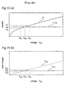
- Figures 15(a) and 15(b) show output current characteristics of the prior art current mirror circuit. More specifically, figure 15(a) shows variations in the output current I 2 when the input current I 1 is constant and the voltage at the output terminal V 2 varies. In figure 15(a), the ratio of the gate width of the FET A11 to the gate width of the FET A12 is 1 : 1.
- Figure 15(b) shows the relationship between the voltage at the input terminal 1 and the voltage at the output terminal 2.
- Figures 17(a)-17(c) are diagrams for explaining drawbacks in the prior art current driver circuit.
- the input signal Sig is an SIN wave of 10GHz.
- the gate width of the FET A11 is 200 ⁇ m, and the gate width of the FET A12 is 600 ⁇ m.
- Figure 17(a) shows the node voltages in the current mirror circuit, wherein the solid line and the dashed line show the signals input to the current mirror circuit from the input buffer 7, the alternate long and short dash line shows the output terminal voltage V (2) , i.e., the drain voltage of the FET A12, and the dotted line shows the input terminal voltage V (1) , i.e., the drain voltage of the FET A11.
- the drain-source voltage of the FET A12 that divides the power supply voltage V SS by resistances varies, whereby the change of the voltage at the output terminal 2 of the current mirror circuit becomes different from the change of the power supply voltage V SS .
- the output current I 2 varies though the input current I 1 is constant, whereby the modulation amplitude varies.
- a current mirror circuit comprises a current input terminal; a first FET and a second FET, each having a gate terminal, a drain terminal, and a source terminal, the gate terminal of the first FET being connected to the gate terminal of the second FET; a third FET having a source terminal connected to the drain terminal of the first FET, and a drain terminal and a gate terminal connected to each other and to the current input terminal; and a fourth FET having a source terminal connected to the drain terminal of the second FET, a gate terminal connected to the gate terminal of the third FET, and a drain terminal serving as a current output terminal.
- the current mirror circuit comprises FETs having high drain conductances, if the output voltage varies, since the current is almost constant, the circuit is not adversely affected by the variation in the output voltage. As a result, an error in the output current in response to the output voltage is significantly reduced.
- the current mirror circuit includes a positive power supply terminal; a negative power supply terminal; the source terminals of the first FET and the second FET being connected to each other and to the negative power supply terminal; a resistor having a first end connected to the source terminal of the first FET and a second end, opposite the first end, connected to the gate terminal of the first FET; a level shift circuit having a low potential end connected to the gate terminal of the first FET, and a high potential end; a fifth FET having a source terminal connected to the high potential end of the level shift circuit, a gate terminal connected to the gate terminal of the third FET, and a drain terminal connected to the positive side power supply terminal; and a current source connected between the positive power supply terminal and the current input terminal.
- the current mirror circuit includes a bypass capacitor connected between the gate terminal of the second FET and the ground. Therefore, the gate voltage of the second FET that is dominant in deciding the output current is made stable, so that distortion in the output current is sufficiently reduced even when the input current includes high frequency noise.
- the current mirror circuit includes a bypass capacitor connected between the gate terminal and the source terminal of the fourth field effect transistor. Therefore, the gate-source voltage of the fourth FET is kept constant for high frequencies, whereby the drain current of the fourth FET is kept constant and the gate-source voltage of the second FET is fixed in view of an equivalent circuit. So, even when the input current is modulated, distortion in the output current is reduced.
- a signal processing circuit comprises a signal processing circuit body including a differential amplifier for differentially amplifying an input signal; and a constant current source for supplying a constant current to the signal processing circuit body, the constant current source comprising the above-mentioned current mirror circuit.
- the modulation current does not depend on the drain conductances of the FETs but depends on the ratio in the gate widths between the FETs, so that the modulation current is controlled with high accuracy, and the production yield of the circuit is improved.
- the signal processing circuit body comprises an input buffer for amplifying a pair of input signals and outputting a pair of output signals; and an open drain circuit including a pair of differential field effect transistors receiving the output signals from the input buffer, the field effect transistors having source terminals connected to each other. Further, the constant current source supplies a constant current to the source terminals of the differential field effect transistors.
- Figure 1 is a diagram illustrating a current mirror circuit in accordance with a first embodiment of the present invention.
- Figures 2(a) and 2(b) are diagrams for explaining DC characteristics of the current mirror circuit according to the first embodiment.
- Figure 3 is a diagram illustrating a current mirror circuit in accordance with a second embodiment of the present invention.
- Figure 4 is a diagram illustrating a current mirror circuit in accordance with a third embodiment of the present invention.
- Figure 5 is a diagram illustrating a current driver circuit employing the current mirror circuit shown in figure 1 as a constant current source, according to a fourth embodiment of the present invention.
- Figures 6(a) and 6(b) are diagrams illustrating node voltages and input and output currents, respectively, in the current driver circuit shown in figure 5, and figure 6(c) is a diagram illustrating an output current from the current driver circuit shown in figure 5.
- Figure 7 is a diagram illustrating modulation current characteristics of the current driver circuit according to the fourth embodiment in comparison with modulation current characteristics of a prior art current driver circuit.
- Figures 8(a) and 8(b) are diagrams illustrating voltage characteristics at nodes in the current driver circuit according to the fourth embodiment.
- Figure 9 is a diagram illustrating a current driver circuit employing the current mirror circuit shown in figure 3 as a constant current source, according to a fifth embodiment of the invention.
- Figures 10(a) and 10(b) are diagrams illustrating node voltages and input and output currents, respectively, in the current driver circuit shown in figure 5, and figure 10(c) is a diagram illustrating an output current from the current driver circuit shown in figure 5, when a high frequency component is superposed on an input current of the current driver circuit.
- Figures 11(a) and 11(b) are diagrams illustrating node voltages and input and output currents, respectively, in the current driver circuit shown in figure 9, and figure 11(c) is a diagram illustrating an output current from the current driver circuit shown in figure 9, when a high frequency component is superposed on an input current of the current driver circuit.
- Figure 12 is a diagram illustrating a current driver circuit employing the current mirror circuit shown in figure 4 as a constant current source, according to a sixth embodiment of the present invention.
- Figures 13(a) and 13(b) are diagrams illustrating node voltages and input and output currents, respectively, in the current driver circuit shown in figure 12, and figure 13(c) is a diagram illustrating an output current from the current driver circuit shown in figure 12.
- Figure 14 is a diagram illustrating a prior art current mirror circuit.
- Figures 15(a) and 15(b) are diagrams for explaining DC characteristics of the prior art current mirror circuit.
- Figure 16 is a diagram illustrating a prior art current driver circuit employing the current mirror circuit shown in figure 14.
- Figures 17(a) and 17(b) are diagrams illustrating node voltages and input and output currents, respectively, in the current driver circuit shown in figure 16, and figure 17(c) is a diagram illustrating an output current from the current driver circuit shown in figure 16.
- Figure 1 is a diagram illustrating a current mirror circuit in accordance with a first embodiment of the present invention.
- the current mirror circuit includes an input terminal I 1 through which a current I 1 flows, an output terminal 2 receiving a current I 2 proportional to the current I 1 , a power supply terminal 5 to which a positive power supply voltage V DD is applied, a power supply terminal 6 to which a negative power supply voltage is applied, and a current source 10 supplying the current I 1 .
- the power supply terminal 6 is connected to the ground GND.
- the current mirror circuit includes enhancement type MESFETs A11, A12, A21, and A22, a level shift circuit LS, and a resistor Z1.
- the MESFETs A11, A12, A21, and A22 are formed in a GaAs IC or the like and have the same gate length and the same threshold voltage V th .
- the level shift circuit LS comprises a single diode or a plurality of diodes connected in series. For example, when a forward bias voltage of the diode is 0.6V, the level shift circuit comprises one diode or two diodes.
- the resistor Z1 is set at a value in a range from 200 ⁇ to 1k ⁇ when a current of 1mA flows through the resistor Z1.
- all the FETs have the same gate length and the same threshold voltage V th .
- a drain terminal and a gate terminal of the FET A21 are short-circuited, and the gate terminal is connected to a gate terminal of the FET A13.
- a source terminal of the FET A21 is connected to a drain terminal of the FET A11.
- a drain terminal of the FET A22 is connected to the output terminal 2, a gate terminal thereof is connected to the drain terminal and the gate terminal of the FET A21 and to the gate terminal of the FET A13, and a source terminal thereof is connected to a drain terminal of the FET A12.
- a source terminal of the FET A11 is connected to the power supply terminal 6.
- An end of the resistor Z1 (first end) is connected to a node between the gate terminals of the FETs A11 and A12 and a low potential end of the level shift circuit LS, and the other end (second end) is connected to the power supply terminal 6.
- a drain terminal of the FET A13 is connected to the power supply terminal 5, and a gate terminal thereof is connected to the drain terminal and the gate terminal of the FET A21 and to the gate terminal of the FET A22.
- a high potential end of the level shift circuit LS is connected to the source terminal of the FET A13, and a low potential end thereof is connected to a node between the first end of the resistor Z1 and the gate terminals of the FETs A11 and A12. Further, a gate terminal of the FET A12 is connected to the gate terminal of the FET A11 and to a node between the low potential end of the level shift circuit LS and the first end of the resistor Z1, and a source terminal thereof is connected to the negative voltage supply terminal 6.
- the power supply terminal 5 is connected to a power supply generating a power supply voltage V DD , and the negative voltage supply terminal 6 is connected to the ground GND. Furthermore, the current supply 10 is connected between the power supply terminal 5 and the input terminal 1.
- the ratio of the gate width of the FET A11 to the gate width of the FET A12 is equal to the ratio of the gate width of the FET A21 to the gate width of the FET A22. Since the FET A21 is an enhancement type FET having a threshold voltage about 0V and the gate and the drain of the FET A21 are short-circuited, it operates in a saturation region ( 0 ⁇ V gs - V th ⁇ V ds ). Therefore, the same gate bias as that applied to the gate electrode of the FET A21 is applied to the gate electrode of the FET A22 which is connected to the gate electrode of the FET A21, so that the FET A22 also operates in the saturation region.
- the FET A11 is originally set so as to operate in the saturation region by the resistor Z1, the level shift circuit LS, and the FET A13. Since the gate electrode of the FET A11 is connected to the gate electrode of the FET A12, the same gate bias as that applied to the FET A11 is applied to the FET A12, so that the FET A12 also operates in the saturation region.
- Figures 2(a) and 2(b) are diagrams for explaining output current characteristics of the current mirror circuit shown in figure 1. These figures show variations in current and voltage when the voltage at the output terminal V 2 varies and the input current I 1 is constant.
- a node between the drain terminal of the FET A11 and the source terminal of the FET A21 is denoted by 3
- a node between the drain terminal of the FET A12 and the source terminal of the FET A22 is denoted by 4 as shown in figure 1.
- the ratio of the gate width of the FET A11 to the gate width of the FET A12 is 1 : 1.
- Figure 2(a) shows the respective currents flowing in the circuit
- figure 2(b) shows the relationship between voltages at the nodes 3 and 4 and the output voltage.
- the terminal voltage V (1) i.e., the gate voltage of the FET A22
- the terminal voltage V (2) i.e., the drain voltage of the FET A22
- the input current I 1 flows as a diode current between the gate and the drain of the FET A22 which has the lowest impedance at this time, so that the current I 3 does not flow through the node 3.
- the terminal voltage V (3) at the node 3, i.e., the terminal voltage V (1) at the input terminal 1, has an offset equivalent to a forward current rising voltage in the diode characteristics of the FET. This offset is about 0.6 V in the figure.
- the terminal voltage V (1) and the terminal voltage V (3) increase while maintaining the offset voltage with an increase in the terminal voltage V (2) at the output terminal 2.
- a current flows through a path comprising the FET A13, the level shift circuit LS, and the resistor Z1 in response to the gate-source voltage of the FET A13, and the gate voltages of the FETs A11 and A12 increase.
- a current I 2 equal to the current I 1 flows through the FET A21, and a voltage equal to the drain-source voltage of the FET A22 produced by the flow of the current I 2 through the FET A22 appears between the drain and the source of the FET A21. Then, a current equal to the current I 1 flowing through the FET A21 flows through the FET A11, and a current equal to the current I 2 flowing through the FET A22 flows through the FET A12. Therefore, a cascade circuit comprising the FETs A11 and A21 and a cascade circuit comprising the FETs A12 and A22 operate under the condition that these FETs have the same drain-source voltage and the same gate bias voltage.
- V (3) is equal to V (4) and I 1 is equal to I 2 , and the FETs A21 and A22 operate as a buffer for the FETs A11 and A12.
- the current mirror circuit since the reference current I 1 and the output current I 2 do not depend on the drain conductance G d of the FET but depend on the gate width of the FET, the current controllability is significantly improved. Further, since the current mirror circuit includes two cascade circuits, each comprising two MESFETs connected in series, a constant current flows even when the output terminal voltage V (2) varies, whereby an output current resistant to variations in the voltage at the output terminal and proportional to the input current can be obtained.
- enhancement type MESFETs are employed in this first embodiment, depletion type MESFETs may be employed with the same effects as described above.
- Figure 3 is a diagram illustrating a current mirror circuit in accordance with the second embodiment of the present invention.
- the current mirror circuit shown in figure 3 is fundamentally identical to the current mirror circuit according to the first embodiment except that a capacitor C1 is connected between the gate terminal of the FET A12 and the ground.
- the input current I 1 applied to the input terminal 1 is a constant current.
- a high frequency component i 1 is superposed on the input current I 1 because of power supply noise.
- bypass capacitor C1 is connected between the gate terminal of the FET A12 and the ground GND, the variation in the gate voltage is suppressed, whereby the output current distortion is sufficiently reduced.
- Figure 4 is a diagram illustrating a current mirror circuit in accordance with a third embodiment of the present invention.
- the current mirror circuit shown in figure 4 is fundamentally identical to the current mirror circuit according to the first embodiment except that a capacitor C2 is connected to the current input terminal 1 at an end and to a node between the source terminal of the FET A22 and the drain terminal of the FET A12 at the other end.
- the drain-source current of the FET A12 is kept constant, whereby the drain-source current of the FET A22 is kept constant.
- the gate-source voltage of the FET A22 is kept constant. Therefore, when the bypass capacitor C2 is connected between the gate and the source of the FET A22, the gate-source voltage of the FET A22 is kept constant for high frequencies, and the drain current of the FET A22 is made constant, whereby the gate-source voltage of the FET A12 is fixed in view of an equivalent circuit.
- bypass capacitor C2 reduces distortion in the output current when the input current is subjected to a modulation.
- Figure 5 is a diagram illustrating an open drain type current driver circuit employing a current mirror circuit according to the first embodiment of the invention as a constant current source for a differential circuit.
- the current driver circuit shown in figure 5 is used in optical communication systems as a driving circuit for a laser diode that converts a current signal to a light signal or a driving circuit for a light modulator that switches transmission and absorption of light in response to an input voltage.
- a driving circuit for a laser diode that converts a current signal to a light signal
- a driving circuit for a light modulator that switches transmission and absorption of light in response to an input voltage.
- the modulation current since the ratio of the magnitude of modulation current to the light output is about 1 : 1, the modulation current must be controlled accurately to obtain specified average light output and extinction coefficient.
- FETs A1 and A2 are differential pair transistors, source terminals of which are connected to each other.
- these FETs A1 and A2 form an open drain circuit 40, i.e., drain terminals thereof are connected to output terminals OUT and OUT ⁇ of the current driver circuit, respectively.
- a load resistor Z2 is connected between the output terminal OUT and the ground terminal GND, and a load resistor Z3 is connected between the output terminal OUT ⁇ and the ground terminal GND.
- An input buffer 7 comprises a differential amplifier (not shown) and a level shift circuit (not shown) and amplifies a pair of input signals to amplitudes required for inputs of the open drain circuit 40, i.e., gate inputs of the FETs A1 and A2.
- a current driver circuit (signal processing circuit) 20 comprises the input buffer 7 and the open drain circuit 40.
- a constant current source 30a comprises a current mirror circuit identical to the current mirror circuit shown in figure 1, and a voltage at the output terminal 2 of the current mirror circuit is equal to a difference between the output level of the output OUT ( OUT ⁇ ) from the input buffer 7 and the gate-source voltage of the FET A1 (FET A2).
- the current driver circuit includes a power supply terminal 5 connected to the ground GND and a power supply terminal 6 connected to a negative terminal of a power supply V SS .
- a positive terminal of the power supply V SS is connected to the ground GND.
- a current I 1 is supplied from the current source 10 to the input terminal 1
- a current I 2 proportional to the current I 1 flows through the source terminals of the FETs A1 and A2 constituting the open drain circuit 40.
- the positive phase input terminal IN of the input buffer 7 is connected to a signal source Sig, and the opposite phase input terminal IN ⁇ of the input buffer 7 is connected to a negative terminal of a reference voltage supply V REF .
- An input signal from the signal source Sig is amplified in the input buffer 7, whereby the FET A1 and the FET A2 alternatingly turn ON and OFF in response to the levels (high and low) of the signal from the signal source Sig and the reference voltage from the reference voltage supply V REF .
- the input signal Sig is a sinusoidal wave of 10GHz.
- the gate width of the FET A11 is 200 ⁇ m, and the gate width of the FET A12 is 600 ⁇ m.
- Figure 6(a) shows the node voltages in the current mirror circuit 30a, wherein the solid line and the dashed line show the signals input to the current mirror circuit from the input buffer 7, the alternate long and short dash line shows the output terminal voltage V (2) , the alternate long and two short dashes line shows the drain voltage V (4) of the FET A12, and the dotted line shows the drain voltage V (3) of the FET A11.
- the drain voltage of the FET A11 is almost equal to the drain voltage of the FET A12.
- Figure 6(c) shows waveforms of output currents from the output terminals OUT and OUT ⁇ of the current driver circuit.
- the drain voltage V (3) is almost equal to the drain voltage V (4)
- the current I 2 is output from the current mirror circuit in response to the ratio of the size of the FET A11 to the size of the FET A12 (1 : 3), i.e., the output current I 2 is 15 mA.
- an error of the output current amplitude from the set value is less than several percents.
- Figure 7 is a diagram for explaining dependence of the modulation current I 2 on the power supply voltage.
- the solid line shows the modulation current obtained in the current driver circuit according to this fourth embodiment
- the dotted line shows the modulation current obtained in the prior art current driver circuit including no power supply voltage compensating circuit.
- the calculated current value on the ordinate is a value obtained by the reference current I 1 and the ratio of the gate width of the FET A11 and the gate width of the FET A12.
- FIGs 8(a) and 8(b) are diagrams illustrating variations in the node voltages in the current mirror circuit when the power supply voltage varies.
- the voltage V (1) at the node 1 increases or decreases in response to the variation in the power supply voltage, i.e., it varies in a range of V SS x 10 %. Therefore, the voltage difference V (1) - V SS , i.e., the drain-source voltage of the reference FET A11 hardly varies.
- the voltage V (2) at the node 2 is almost constant regardless of the variation in the power supply voltage, the drain-source voltage of the FET A12 varies. As a result, the output current I 2 varies.
- a current mirror circuit according to the first embodiment of the invention is used as a constant current source 30a for the current driver circuit 20 comprising the input buffer 7 and the open drain circuit 40, and a current output terminal of the current mirror circuit is connected to the sources of the MESFETs A1 and A2 constituting the open drain circuit 40. Therefore, the modulation current does not depend on the drain conductances of the FETs but depends on the gate width ratio between the FETs, whereby the current controllability is improved and the production yield of the circuit is increased.
- Figure 9 is a diagram illustrating an open drain type current driver circuit employing a current mirror circuit according to the second embodiment of the invention as a constant current source for a differential circuit, according to a fifth embodiment of the present invention.
- reference numeral 30b designates a constant current source comprising a current mirror circuit similar to the current mirror circuit shown in figure 3.
- the voltage at the output terminal 2 is equal to a difference between the output level at the output terminal OUT ( OUT ⁇ ) of the input buffer 7 and the gate-source voltage of the FET A1 (FET A2).
- a bypass capacitor C1 is connected between the gate terminal of the FET A12 and the ground GND, whereby distortion in output current characteristics is reduced.
- a high frequency component i 1 is superposed on the input current I 1 because of power supply noise.
- Figures 10(a), 10(b), and 10(c) are diagrams illustrating the node voltage, the input and output currents I 1 and I 2 , and the output current from the driver circuit, respectively, when a high frequency component is superposed on the input current I 1 in the current mirror circuit in the current driver circuit according to the fourth embodiment.
- the input signal Sig is a sinusoidal wave of 10 GHz.
- the gate width of the FET A11 in the current mirror circuit is 200 ⁇ m, and the gate width of the FET A12 is 600 ⁇ m.
- the input current I 1 is 5 mA, and the high frequency component is ⁇ 1 mA and a sinusoidal wave of 10 GHz.
- Figure 10(a) shows the gate voltage of the FET A12.
- Figure 10(c) shows the output current waveform from the output terminals OUT and OUT ⁇ of the driver circuit.
- figures 11(a), 11(b), and 11(c) are diagrams illustrating the node voltage, the input and output currents I 1 and I 2 , and the output current from the driver circuit, respectively, when a high frequency component is superposed on the input current I 1 in the current mirror circuit in the current driver circuit according to this fifth embodiment.
- the input signal Sig is a sinusoidal wave of 10 GHz.
- the gate width of the FET A11 in the current mirror circuit is 200 ⁇ m, and the gate width of the FET A12 is 600 ⁇ m.
- the input current I 1 is 5 mA, and the high frequency component is ⁇ 1 mA.
- the bypass capacitor C1 is 40 pF.
- Figure 11(a) shows the gate voltage of the FET A12.
- Figure 11(c) shows a waveform of the output current from the output terminals OUT and OUT ⁇ of the driver circuit.
- the variation in the output current I 2 from the current mirror circuit is less than 1 mA, whereby the symmetry of the output current amplitude from the driver circuit is significantly improved.
- the constant current source 30b having the bypass capacitor C1 can sufficiently reduce the distortion in the output current, and the signal processing circuit employing this constant current source 30b is hardly affected by the power supply noise.
- the bypass capacitor C1 is connected between the gate terminal of the FET A12, which is an constituent of the constant current source 30b, and the ground GND, variations in the gate voltage are suppressed, whereby distortion in output current characteristics of the constant current source 30b is reduced. Therefore, the signal processing circuit including this constant current source 30b is hardly affected by power supply noise, whereby the modulation current is controlled with high accuracy.
- Figure 12 is a diagram illustrating an open drain type current driver circuit employing a current mirror circuit according to the third embodiment of the invention as a constant current source for a differential circuit, according to a sixth embodiment of the present invention.
- reference numeral 30c designates a constant current source comprising a current mirror circuit similar to the current mirror circuit shown in figure 4.
- the voltage at the output terminal 2 is equal to a difference between the output level at the output terminal OUT ( OUT ⁇ ) of the input buffer 7 and the gate-source voltage of the FET A1 (FET A2).
- a bypass capacitor C2 is connected between the gate terminal and the source terminal of the FET A22, whereby distortion in output current characteristics is reduced.
- the bypass capacitor C1 since the bypass capacitor C1 is connected to the FET A12 in the constant current source 30b, the drain-source current of the FET A12 is kept constant, whereby the drain-source current of the FET A22 is kept constant. In other words, the gate-source voltage of the FET A22 is kept constant. Therefore, when the bypass capacitor C2 is connected between the gate and the source of the FET A22, the gate-source voltage of the FET A22 is kept constant for high frequencies, and the drain current of the FET A22 is made constant, whereby the gate-source potential of the FET A12 is fixed in view of an equivalent circuit.
- Figures 13(a), 13(b), and 13(c) are diagrams illustrating a node voltage, input and output currents I 1 and I 2 , and an output current from the driver circuit, respectively, when a high frequency component is superposed on the input current I 1 in the current mirror circuit in the current driver circuit according to this sixth embodiment.
- the input signal Sig is a sinusoidal wave of 10 GHz.
- the gate width of the FET A11 in the current mirror circuit is 200 ⁇ m, and the gate width of the FET A12 is 600 ⁇ m.
- the input current I 1 is 5 mA, and the high frequency component is ⁇ 1 mA.
- the bypass capacitor C2 is 40 pF.
- Figure 13(a) shows the gate voltage of the FET A12.
- Figure 13(c) shows waveforms of the output current from the output terminals OUT and OUT ⁇ of the driver circuit.
- the variation in the output current I 2 from the current mirror circuit is reduced, whereby the symmetry of the output current amplitude in the driver circuit is significantly improved.
- bypass capacitor C2 can reduce distortion in output current when the input current is subjected to modulation.
- the constant current source 30c including the bypass capacitor C2 can sufficiently reduce distortion in output current, and the signal processing circuit including this constant current source 30c is hardly affected by power supply noise.
- bypass capacitor C2 is connected between the gate terminal and the source terminal of the FET A12 which is an constituent of the constant current source 30c, variations in the gate voltage are suppressed, whereby distortion in output current characteristics of the constant current source 30c is reduced. Therefore, the signal processing circuit including the constant current source 30c is hardly affected by power supply noise, whereby the modulation current is controlled with high accuracy.
Abstract
Description
- The present invention relates to a semiconductor circuit including field effect transistors (hereinafter referred to as FETs) and, more particularly, to a current mirror circuit having electrical characteristics independent of drain conductances of the FETs. The present invention also relates to a signal processing circuit employing the current mirror circuit.
- Figure 14 is a diagram illustrating a prior art current mirror circuit. The current mirror circuit includes an
input terminal 1 through which a current I1 flows, anoutput terminal 2 receiving a current I2 proportional to the current I1, apower supply terminal 5 to which a positive power supply voltage VDD is applied, apower supply terminal 6 to which a negative power supply voltage is applied, and acurrent source 10 supplying the current I1. Thepower supply terminal 6 is connected to the ground GND. Further, the current mirror circuit includes enhancement type MESFETs A11, A12, and A13, a level shift circuit LS, and a resistor Z1. The MESFETs A11, A12, and A13 are formed in a GaAs integrated circuit (hereinafter referred to as GaAs IC) or the like and have the same gate length and the same threshold voltage Vth. The level shift circuit LS comprises a single diode or a plurality of diodes connected in series. For example, when a forward bias voltage of the diode is 0.6V, the level shift circuit comprises one diode or two diodes. The resistor Z1 is set at a value in a range from 200Ω to 1kΩ when a current of 1mA flows through the resistor Z1. - In the prior art current mirror circuit shown in figure 14, a drain terminal of the FET A11 is connected to the
input terminal 1, and a source terminal thereof is connected to the negativepower supply terminal 6. An end (first end) of the resistor Z1 is connected to a gate terminal of the FET A11, and the other end thereof (second end) is connected to thepower supply terminal 6. A drain terminal of the FET A13 is connected to the positivepower supply terminal 5, and a gate terminal thereof is connected to the drain terminal of the FET A11. A high potential end of the level shift circuit LS is connected to a source terminal of the FET A13, and a low potential end thereof is connected to a node between the first end of the resistor Z1 and the gate terminals of the FETs A11 and A12. Further, a drain terminal of the FET A12 is connected to theoutput terminal 2, a gate terminal thereof is connected to the gate terminal of the FET A11 and to a node between the low potential end of the level shift circuit LS and the first end of the resistor Z1, and a source electrode thereof is connected to thepower supply terminal 6. Furthermore, thepower supply terminal 5 is connected to a power source generating the power supply voltage VDD, and thepower supply terminal 6 is connected to the ground GND. Thecurrent supply 10 is connected between thepower supply terminal 5 and theinput terminal 1. - A description is given of the operation. Since the input impedance of the MESFET viewed from the gate is large, the current I1 from the
current source 10 does not flow into the gate of the FET A13 but flows into the drain terminal of the FET A11. Since the FET A11 is an enhancement type MESFET (Vth > 0) and the drain-source current Ids is equal to the current I1 (> 0), the gate-source voltage Vgs is larger than 0, so that a current flows through the resistor Z1 connected between the gate and the source of the FET A11 and, simultaneously, a current flows through the level shift circuit LS. - Since the level shift circuit LS comprises a single diode or a plurality of diodes connected in series, when a forward current flows through the level shift circuit LS, a constant forward voltage is generated, whereby the source potential of the FET A13 increases. Further, when a current flows through the level shift circuit LS and a drain current flows through the FET A13 connected to the level shift circuit LS, since the gate-source voltage of the FET A13 is positive, the gate potential of the FET A13, i.e., the drain voltage of the FET A11, increases. At this time, in order to make the FET A11 operate in a saturation region, the level shift quantity of the level shift circuit LS is adjusted in advance by, for example, connecting a plurality of diodes in series. Thereby, the drain-source current Ids of the FET A11 in the saturation region (


- On the other hand, the drain terminal of the FET A12 is connected to the
output terminal 2, the source terminal thereof is connected to thepower supply terminal 6, and the gate terminal thereof is connected to a node between the FET A11 and the resistor Z1. When the ratio of the gate width of the FET A11 to the gate width of the FET A12 is 1 : m (m > 0) and a voltage that makes the FET A12 operate in the saturation region is applied to theoutput terminal 2, the drain current of the FET A12, i.e., the output current I2, is given by

- In equation (2), when the drain conductance

output terminal 2 is given by
- Figure 16 is a diagram illustrating a prior art current driver circuit using a current mirror circuit identical to the current mirror circuit shown in figure 14 as a constant current source and including a differential amplifier that has two inputs and produces an output signal that is a function of the difference between the inputs. In the figure, FETs A1 and A2 are differential pair transistors, source terminals of which are connected to each other. In addition, these FETs A1 and A2 form an
open drain circuit 40, i.e., drain terminals thereof are connected to output terminals OUT and

input buffer 7 comprises a differential amplifier (not shown) and a level shift circuit (not shown) and amplifies a pair of input signals to amplitudes required for inputs of theopen drain circuit 40, i.e., gate inputs of the FETs A1 and A2. Acurrent driver circuit 20 comprises theinput buffer 7 and theopen drain circuit 40. A constantcurrent source 30 comprises a current mirror circuit identical to the current mirror circuit shown in figure 14, and a voltage at anoutput terminal 2 of the current mirror circuit is equal to a difference between the output level of the output OUT (
input buffer 7 and the gate-source voltage of the FET A1 (FET A2). Furthermore, the current driver circuit includes apower supply terminal 5 connected to the ground GND and apower supply terminal 6 connected to a negative terminal of a power supply VSS. A positive terminal of the power supply VSS is connected to the ground GND. - A description is given of the operation. When a current I1 from the
current source 10 is applied to theinput terminal 1, a current I2 proportional to the current I1 flows through the source terminals of the FETs A1 and A2 constituting theopen drain circuit 40. The positive phase input terminal IN of theinput buffer 7 is connected to a signal source Sig, and the opposite phase input terminal
input buffer 7 is connected to a negative terminal of a reference voltage supply VREF. An input signal from the signal source Sig is amplified in theinput buffer 7, whereby the FET A1 and the FET A2 alternatingly turn ON and OFF in response to the level of the signal voltage from the signal source Sig and the level of the reference voltage from the reference voltage supply VREF. By the alternating ON and OFF switching of the FETs A1 and A2, the current path of the current I2 is changed, and a modulation current having an amplitude equivalent to that of the current I2 is output from the output terminals OUT and
- In the prior art current mirror circuit shown in figure 14, however, substantial drain conductances of the MESFETs are large and adversely affect the circuit characteristics. Figures 15(a) and 15(b) show output current characteristics of the prior art current mirror circuit. More specifically, figure 15(a) shows variations in the output current I2 when the input current I1 is constant and the voltage at the output terminal V2 varies. In figure 15(a), the ratio of the gate width of the FET A11 to the gate width of the FET A12 is 1 : 1. Figure 15(b) shows the relationship between the voltage at the
input terminal 1 and the voltage at theoutput terminal 2. - In the circuit structure shown in figure 14, since a constant gate voltage is given to the FET A12, the I2 - V2 characteristics are identical to the Ids - Vds characteristics of the single FET A12 itself. Only when V1 is equal to V2 (V2b in the figure), I1 is equal to I2, i.e., the current ratio is equal to the gate width ratio.
- As described above, in the prior art current mirror circuit, since only the gate-source voltage of the FET A12 through which the input current I1 flows is secured for the input current I1, the voltage at the
output terminal 2 varies in an element having a high drain conductance, resulting in an error in the output current I2. - Furthermore, in the prior art current driver circuit including the current mirror circuit as a constant current source, since the output terminal voltage V(2) of the current mirror circuit depends on the output voltage from the
input buffer 7, the output terminal voltage V(2) is not always equal to the input terminal voltage V(1), so that the modulation current I2 has an error with respect to the constant reference current I1. - Figures 17(a)-17(c) are diagrams for explaining drawbacks in the prior art current driver circuit. In the current driver circuit, the input signal Sig is an SIN wave of 10GHz. The gate width of the FET A11 is 200 µm, and the gate width of the FET A12 is 600 µm. Figure 17(a) shows the node voltages in the current mirror circuit, wherein the solid line and the dashed line show the signals input to the current mirror circuit from the
input buffer 7, the alternate long and short dash line shows the output terminal voltage V(2), i.e., the drain voltage of the FET A12, and the dotted line shows the input terminal voltage V(1), i.e., the drain voltage of the FET A11. As shown in figure 17(a), a difference between the drain voltage V(1) of the FET A11 and the drain voltage V(2) of the FET A12 is about 1.5 V. Figure 17(b) shows the input current I1 and the output current I2 of the current mirror circuit, wherein the solid line shows the input current I1 (= 5 mA) and the dashed line shows the output current I2. Figure 17(c) shows waveforms of the output currents from the output terminals OUT and
- Further, when the power supply voltage VSS varies, the drain-source voltage of the FET A12 that divides the power supply voltage VSS by resistances varies, whereby the change of the voltage at the
output terminal 2 of the current mirror circuit becomes different from the change of the power supply voltage VSS. As the result, the output current I2 varies though the input current I1 is constant, whereby the modulation amplitude varies. - In order to prevent the above-mentioned problems in the prior art current driver circuit, it is necessary to cancel the variation in the modulation amplitude using a power supply voltage compensation circuit which monitors the output amplitude of the current driver circuit (for example, the output amplitude at the output terminal

- It is an object of the present invention to provide a current mirror circuit that can suppress an error in an output current in response to an output voltage even when the circuit comprises semiconductor elements having high drain conductances.
- It is another object of the present invention to provide a signal processing circuit that can suppress a variation in a modulation amplitude without a power supply voltage compensation circuit.
- Other objects and advantages of the invention will become apparent from the detailed description that follows. The detailed description and specific embodiments described are provided only for illustration since various additions and modifications within the scope of the invention will be apparent to those of skill in the art from the detailed description.
- According to a first aspect of the present invention, a current mirror circuit comprises a current input terminal; a first FET and a second FET, each having a gate terminal, a drain terminal, and a source terminal, the gate terminal of the first FET being connected to the gate terminal of the second FET; a third FET having a source terminal connected to the drain terminal of the first FET, and a drain terminal and a gate terminal connected to each other and to the current input terminal; and a fourth FET having a source terminal connected to the drain terminal of the second FET, a gate terminal connected to the gate terminal of the third FET, and a drain terminal serving as a current output terminal. Therefore, when the current mirror circuit comprises FETs having high drain conductances, if the output voltage varies, since the current is almost constant, the circuit is not adversely affected by the variation in the output voltage. As a result, an error in the output current in response to the output voltage is significantly reduced.
- According to a second aspect of the present invention, the current mirror circuit includes a positive power supply terminal; a negative power supply terminal; the source terminals of the first FET and the second FET being connected to each other and to the negative power supply terminal; a resistor having a first end connected to the source terminal of the first FET and a second end, opposite the first end, connected to the gate terminal of the first FET; a level shift circuit having a low potential end connected to the gate terminal of the first FET, and a high potential end; a fifth FET having a source terminal connected to the high potential end of the level shift circuit, a gate terminal connected to the gate terminal of the third FET, and a drain terminal connected to the positive side power supply terminal; and a current source connected between the positive power supply terminal and the current input terminal.
- According to a third aspect of the present invention, the current mirror circuit includes a bypass capacitor connected between the gate terminal of the second FET and the ground. Therefore, the gate voltage of the second FET that is dominant in deciding the output current is made stable, so that distortion in the output current is sufficiently reduced even when the input current includes high frequency noise.
- According to a fourth aspect of the present invention, the current mirror circuit includes a bypass capacitor connected between the gate terminal and the source terminal of the fourth field effect transistor. Therefore, the gate-source voltage of the fourth FET is kept constant for high frequencies, whereby the drain current of the fourth FET is kept constant and the gate-source voltage of the second FET is fixed in view of an equivalent circuit. So, even when the input current is modulated, distortion in the output current is reduced.
- According to a fifth aspect of the present invention, a signal processing circuit comprises a signal processing circuit body including a differential amplifier for differentially amplifying an input signal; and a constant current source for supplying a constant current to the signal processing circuit body, the constant current source comprising the above-mentioned current mirror circuit. In this case, the modulation current does not depend on the drain conductances of the FETs but depends on the ratio in the gate widths between the FETs, so that the modulation current is controlled with high accuracy, and the production yield of the circuit is improved. Further, when the power supply voltage varies, since the variations in the voltages at the node between the first FET and the second FET and at the node between the second FET and the fourth FET are approximately equal to the variation in the power supply voltage, the output current does not vary even though the voltage at the output terminal of the current mirror circuit varies. Therefore, a compensating circuit is dispensed with, and the size of the circuit is reduced.
- According to a sixth aspect of the present invention, the signal processing circuit body comprises an input buffer for amplifying a pair of input signals and outputting a pair of output signals; and an open drain circuit including a pair of differential field effect transistors receiving the output signals from the input buffer, the field effect transistors having source terminals connected to each other. Further, the constant current source supplies a constant current to the source terminals of the differential field effect transistors.
- Figure 1 is a diagram illustrating a current mirror circuit in accordance with a first embodiment of the present invention.
- Figures 2(a) and 2(b) are diagrams for explaining DC characteristics of the current mirror circuit according to the first embodiment.
- Figure 3 is a diagram illustrating a current mirror circuit in accordance with a second embodiment of the present invention.
- Figure 4 is a diagram illustrating a current mirror circuit in accordance with a third embodiment of the present invention.
- Figure 5 is a diagram illustrating a current driver circuit employing the current mirror circuit shown in figure 1 as a constant current source, according to a fourth embodiment of the present invention.
- Figures 6(a) and 6(b) are diagrams illustrating node voltages and input and output currents, respectively, in the current driver circuit shown in figure 5, and figure 6(c) is a diagram illustrating an output current from the current driver circuit shown in figure 5.
- Figure 7 is a diagram illustrating modulation current characteristics of the current driver circuit according to the fourth embodiment in comparison with modulation current characteristics of a prior art current driver circuit.
- Figures 8(a) and 8(b) are diagrams illustrating voltage characteristics at nodes in the current driver circuit according to the fourth embodiment.
- Figure 9 is a diagram illustrating a current driver circuit employing the current mirror circuit shown in figure 3 as a constant current source, according to a fifth embodiment of the invention.
- Figures 10(a) and 10(b) are diagrams illustrating node voltages and input and output currents, respectively, in the current driver circuit shown in figure 5, and figure 10(c) is a diagram illustrating an output current from the current driver circuit shown in figure 5, when a high frequency component is superposed on an input current of the current driver circuit.
- Figures 11(a) and 11(b) are diagrams illustrating node voltages and input and output currents, respectively, in the current driver circuit shown in figure 9, and figure 11(c) is a diagram illustrating an output current from the current driver circuit shown in figure 9, when a high frequency component is superposed on an input current of the current driver circuit.
- Figure 12 is a diagram illustrating a current driver circuit employing the current mirror circuit shown in figure 4 as a constant current source, according to a sixth embodiment of the present invention.
- Figures 13(a) and 13(b) are diagrams illustrating node voltages and input and output currents, respectively, in the current driver circuit shown in figure 12, and figure 13(c) is a diagram illustrating an output current from the current driver circuit shown in figure 12.
- Figure 14 is a diagram illustrating a prior art current mirror circuit.
- Figures 15(a) and 15(b) are diagrams for explaining DC characteristics of the prior art current mirror circuit.
- Figure 16 is a diagram illustrating a prior art current driver circuit employing the current mirror circuit shown in figure 14.
- Figures 17(a) and 17(b) are diagrams illustrating node voltages and input and output currents, respectively, in the current driver circuit shown in figure 16, and figure 17(c) is a diagram illustrating an output current from the current driver circuit shown in figure 16.
- Figure 1 is a diagram illustrating a current mirror circuit in accordance with a first embodiment of the present invention. In the figure, the current mirror circuit includes an input terminal I1 through which a current I1 flows, an
output terminal 2 receiving a current I2 proportional to the current I1, apower supply terminal 5 to which a positive power supply voltage VDD is applied, apower supply terminal 6 to which a negative power supply voltage is applied, and acurrent source 10 supplying the current I1. Thepower supply terminal 6 is connected to the ground GND. Further, the current mirror circuit includes enhancement type MESFETs A11, A12, A21, and A22, a level shift circuit LS, and a resistor Z1. The MESFETs A11, A12, A21, and A22 are formed in a GaAs IC or the like and have the same gate length and the same threshold voltage Vth. The level shift circuit LS comprises a single diode or a plurality of diodes connected in series. For example, when a forward bias voltage of the diode is 0.6V, the level shift circuit comprises one diode or two diodes. The resistor Z1 is set at a value in a range from 200Ω to 1kΩ when a current of 1mA flows through the resistor Z1. - In this current mirror circuit, all the FETs have the same gate length and the same threshold voltage Vth. A drain terminal and a gate terminal of the FET A21 are short-circuited, and the gate terminal is connected to a gate terminal of the FET A13. A source terminal of the FET A21 is connected to a drain terminal of the FET A11. A drain terminal of the FET A22 is connected to the
output terminal 2, a gate terminal thereof is connected to the drain terminal and the gate terminal of the FET A21 and to the gate terminal of the FET A13, and a source terminal thereof is connected to a drain terminal of the FET A12. - Further, a source terminal of the FET A11 is connected to the
power supply terminal 6. An end of the resistor Z1 (first end) is connected to a node between the gate terminals of the FETs A11 and A12 and a low potential end of the level shift circuit LS, and the other end (second end) is connected to thepower supply terminal 6. A drain terminal of the FET A13 is connected to thepower supply terminal 5, and a gate terminal thereof is connected to the drain terminal and the gate terminal of the FET A21 and to the gate terminal of the FET A22. A high potential end of the level shift circuit LS is connected to the source terminal of the FET A13, and a low potential end thereof is connected to a node between the first end of the resistor Z1 and the gate terminals of the FETs A11 and A12. Further, a gate terminal of the FET A12 is connected to the gate terminal of the FET A11 and to a node between the low potential end of the level shift circuit LS and the first end of the resistor Z1, and a source terminal thereof is connected to the negativevoltage supply terminal 6. Thepower supply terminal 5 is connected to a power supply generating a power supply voltage VDD, and the negativevoltage supply terminal 6 is connected to the ground GND. Furthermore, thecurrent supply 10 is connected between thepower supply terminal 5 and theinput terminal 1. - A description is given of the operation. The ratio of the gate width of the FET A11 to the gate width of the FET A12 is equal to the ratio of the gate width of the FET A21 to the gate width of the FET A22. Since the FET A21 is an enhancement type FET having a threshold voltage about 0V and the gate and the drain of the FET A21 are short-circuited, it operates in a saturation region (

- Further, the FET A11 is originally set so as to operate in the saturation region by the resistor Z1, the level shift circuit LS, and the FET A13. Since the gate electrode of the FET A11 is connected to the gate electrode of the FET A12, the same gate bias as that applied to the FET A11 is applied to the FET A12, so that the FET A12 also operates in the saturation region.
- Figures 2(a) and 2(b) are diagrams for explaining output current characteristics of the current mirror circuit shown in figure 1. These figures show variations in current and voltage when the voltage at the output terminal V2 varies and the input current I1 is constant. Hereinafter, a node between the drain terminal of the FET A11 and the source terminal of the FET A21 is denoted by 3, and a node between the drain terminal of the FET A12 and the source terminal of the FET A22 is denoted by 4 as shown in figure 1. In addition, the ratio of the gate width of the FET A11 to the gate width of the FET A12 is 1 : 1.
- Figure 2(a) shows the respective currents flowing in the circuit, and figure 2(b) shows the relationship between voltages at the
nodes output terminal 2 is not higher than 0.6 V, the terminal voltage V(1), i.e., the gate voltage of the FET A22, is higher than the terminal voltage V(2), i.e., the drain voltage of the FET A22, and the input current I1 flows as a diode current between the gate and the drain of the FET A22 which has the lowest impedance at this time, so that the current I3 does not flow through thenode 3. Thereby, the terminal voltage V(3) at thenode 3, i.e., the terminal voltage V(1) at theinput terminal 1, has an offset equivalent to a forward current rising voltage in the diode characteristics of the FET. This offset is about 0.6 V in the figure. The terminal voltage V(1) and the terminal voltage V(3) increase while maintaining the offset voltage with an increase in the terminal voltage V(2) at theoutput terminal 2. After the terminal voltage V(2) exceeds about 0.7 V, a current flows through a path comprising the FET A13, the level shift circuit LS, and the resistor Z1 in response to the gate-source voltage of the FET A13, and the gate voltages of the FETs A11 and A12 increase. When the FETs A11 and A12 turn on and the impedance reduces, a drain current flows through this path and, simultaneously, a current flows between the drain and the source of the FET A21 and between the drain and the source of the FET A22. When the terminal voltage V(2) at theoutput terminal 2 becomes equal to the terminal voltage V(1) at the input terminal 1 (in figure 2(b),


- When these FETs A11, A12, A21, and A22 operate under the same condition mentioned above, V(3) is equal to V(4) and I1 is equal to I2, and the FETs A21 and A22 operate as a buffer for the FETs A11 and A12.
- This buffer functions as follows. That is, as illustrated in figure 2(b), when V(2) exceeds V2b and increases, if the drain conductance of the FET A22 is Gd and the transconductance thereof is


node 4 hardly changes though the output terminal voltage V(2) increases. - Therefore, even in a range of V(2) > V(1) (for example, V2c in figure 2(b)), since V(4) is equal to V(3),

output terminal 2 and proportional to the input current is obtained. - As described above, in the current mirror circuit according to the first embodiment of the invention, since the reference current I1 and the output current I2 do not depend on the drain conductance Gd of the FET but depend on the gate width of the FET, the current controllability is significantly improved. Further, since the current mirror circuit includes two cascade circuits, each comprising two MESFETs connected in series, a constant current flows even when the output terminal voltage V(2) varies, whereby an output current resistant to variations in the voltage at the output terminal and proportional to the input current can be obtained.
- Although enhancement type MESFETs are employed in this first embodiment, depletion type MESFETs may be employed with the same effects as described above.
- Figure 3 is a diagram illustrating a current mirror circuit in accordance with the second embodiment of the present invention. The current mirror circuit shown in figure 3 is fundamentally identical to the current mirror circuit according to the first embodiment except that a capacitor C1 is connected between the gate terminal of the FET A12 and the ground.
- In the first embodiment of the invention, it is assumed that the input current I1 applied to the
input terminal 1 is a constant current. In an actual IC, however, a high frequency component i1 is superposed on the input current I1 because of power supply noise. In the current mirror circuit, the high frequency component i1 in the input current I1 is amplified at the ratio m (m > 0) of the gate widths between the FETs, and a high frequency component
- By the way, in the current mirror circuit according to the first embodiment, the output current I2 depends on both the gate voltage and the drain voltage of the FET A12, but the variation in the gate voltage dominates the output current distortion because a relationship of


- In this second embodiment of the invention, since the bypass capacitor C1 is connected between the gate terminal of the FET A12 and the ground GND, the variation in the gate voltage is suppressed, whereby the output current distortion is sufficiently reduced.
- Figure 4 is a diagram illustrating a current mirror circuit in accordance with a third embodiment of the present invention. The current mirror circuit shown in figure 4 is fundamentally identical to the current mirror circuit according to the first embodiment except that a capacitor C2 is connected to the
current input terminal 1 at an end and to a node between the source terminal of the FET A22 and the drain terminal of the FET A12 at the other end. - When the bypass capacitor C1 is used in the second embodiment of the invention, the drain-source current of the FET A12 is kept constant, whereby the drain-source current of the FET A22 is kept constant. In other words, the gate-source voltage of the FET A22 is kept constant. Therefore, when the bypass capacitor C2 is connected between the gate and the source of the FET A22, the gate-source voltage of the FET A22 is kept constant for high frequencies, and the drain current of the FET A22 is made constant, whereby the gate-source voltage of the FET A12 is fixed in view of an equivalent circuit.
- In this way, the bypass capacitor C2 reduces distortion in the output current when the input current is subjected to a modulation.
- Figure 5 is a diagram illustrating an open drain type current driver circuit employing a current mirror circuit according to the first embodiment of the invention as a constant current source for a differential circuit.
- The current driver circuit shown in figure 5 is used in optical communication systems as a driving circuit for a laser diode that converts a current signal to a light signal or a driving circuit for a light modulator that switches transmission and absorption of light in response to an input voltage. In this case, since the ratio of the magnitude of modulation current to the light output is about 1 : 1, the modulation current must be controlled accurately to obtain specified average light output and extinction coefficient.
- In figure 5, FETs A1 and A2 are differential pair transistors, source terminals of which are connected to each other. In addition, these FETs A1 and A2 form an
open drain circuit 40, i.e., drain terminals thereof are connected to output terminals OUT and

input buffer 7 comprises a differential amplifier (not shown) and a level shift circuit (not shown) and amplifies a pair of input signals to amplitudes required for inputs of theopen drain circuit 40, i.e., gate inputs of the FETs A1 and A2. A current driver circuit (signal processing circuit) 20 comprises theinput buffer 7 and theopen drain circuit 40. A constantcurrent source 30a comprises a current mirror circuit identical to the current mirror circuit shown in figure 1, and a voltage at theoutput terminal 2 of the current mirror circuit is equal to a difference between the output level of the output OUT (
input buffer 7 and the gate-source voltage of the FET A1 (FET A2). Furthermore, the current driver circuit includes apower supply terminal 5 connected to the ground GND and apower supply terminal 6 connected to a negative terminal of a power supply VSS. A positive terminal of the power supply VSS is connected to the ground GND. - A description is give of the operation. When a current I1 is supplied from the
current source 10 to theinput terminal 1, a current I2 proportional to the current I1 flows through the source terminals of the FETs A1 and A2 constituting theopen drain circuit 40. The positive phase input terminal IN of theinput buffer 7 is connected to a signal source Sig, and the opposite phase input terminal
input buffer 7 is connected to a negative terminal of a reference voltage supply VREF. An input signal from the signal source Sig is amplified in theinput buffer 7, whereby the FET A1 and the FET A2 alternatingly turn ON and OFF in response to the levels (high and low) of the signal from the signal source Sig and the reference voltage from the reference voltage supply VREF. By the alternating ON and OFF switching of the FETs A1 and A2, the current path of the current I2 is changed, and a modulation current having an amplitude equivalent to that of the current I2 is output from the output terminals OUT and
- In this current driver circuit, the input signal Sig is a sinusoidal wave of 10GHz. The gate width of the FET A11 is 200 µm, and the gate width of the FET A12 is 600 µm.
- Figure 6(a) shows the node voltages in the
current mirror circuit 30a, wherein the solid line and the dashed line show the signals input to the current mirror circuit from theinput buffer 7, the alternate long and short dash line shows the output terminal voltage V(2), the alternate long and two short dashes line shows the drain voltage V(4) of the FET A12, and the dotted line shows the drain voltage V(3) of the FET A11. In the driver circuit according to this fourth embodiment, the drain voltage of the FET A11 is almost equal to the drain voltage of the FET A12. Figure 6(b) shows the input current I1 and the output current I2 of the current mirror circuit, wherein the solid line shows the input current I1 (= 5 mA) and the dashed line shows the output current I2. Figure 6(c) shows waveforms of output currents from the output terminals OUT and
- Figure 7 is a diagram for explaining dependence of the modulation current I2 on the power supply voltage. In the figure, the solid line shows the modulation current obtained in the current driver circuit according to this fourth embodiment, and the dotted line shows the modulation current obtained in the prior art current driver circuit including no power supply voltage compensating circuit. In addition, the calculated current value on the ordinate is a value obtained by the reference current I1 and the ratio of the gate width of the FET A11 and the gate width of the FET A12.
- In figure 7, when the supply voltage VSS varies by ±5 %, the current I2 also varies by about ±5 % in the prior art circuit. However, in the circuit according to this fourth embodiment using the same FET parameters, the current I2 is almost constant and approximates to the calculated value.
- Figures 8(a) and 8(b) are diagrams illustrating variations in the node voltages in the current mirror circuit when the power supply voltage varies. In the prior art circuit, as shown in figure 8(b), when the power supply voltage VSS varies by ±5 %, the voltage V(1) at the node 1 (see figure 14) increases or decreases in response to the variation in the power supply voltage, i.e., it varies in a range of VSS x 10 %. Therefore, the voltage difference V(1) - VSS, i.e., the drain-source voltage of the reference FET A11 hardly varies. However, since the voltage V(2) at the node 2 (see figure 14) is almost constant regardless of the variation in the power supply voltage, the drain-source voltage of the FET A12 varies. As a result, the output current I2 varies.
- On the other hand, in the current driver circuit according to this fourth embodiment, as shown in figure 8(a), although the voltage at the
node 1 is constant as in the prior art circuit, since the drain voltages of both the FET A11 and the FET A12 increase or decrease by the variation in the power supply voltage, the drain-source voltages of these FETs are always constant. Therefore, the ratio of the current I1 to the current I2 is constant even when the power supply voltage varies. - In this fourth embodiment of the invention, a current mirror circuit according to the first embodiment of the invention is used as a constant
current source 30a for thecurrent driver circuit 20 comprising theinput buffer 7 and theopen drain circuit 40, and a current output terminal of the current mirror circuit is connected to the sources of the MESFETs A1 and A2 constituting theopen drain circuit 40. Therefore, the modulation current does not depend on the drain conductances of the FETs but depends on the gate width ratio between the FETs, whereby the current controllability is improved and the production yield of the circuit is increased. Further, when the power supply voltage VSS varies, since variations in voltages at thenodes output terminal 2 of the current mirror circuit varies. Therefore, a circuit for compensating the variation in the voltage at the output terminal is not necessary, resulting in a reduction in the circuit size. - Figure 9 is a diagram illustrating an open drain type current driver circuit employing a current mirror circuit according to the second embodiment of the invention as a constant current source for a differential circuit, according to a fifth embodiment of the present invention.
- In the figure,
reference numeral 30b designates a constant current source comprising a current mirror circuit similar to the current mirror circuit shown in figure 3. In the current mirror circuit, the voltage at theoutput terminal 2 is equal to a difference between the output level at the output terminal OUT (
input buffer 7 and the gate-source voltage of the FET A1 (FET A2). - In the constant
current source 30b, a bypass capacitor C1 is connected between the gate terminal of the FET A12 and the ground GND, whereby distortion in output current characteristics is reduced. - In an actual IC, a high frequency component i1 is superposed on the input current I1 because of power supply noise. In the current mirror circuit, the high frequency component i1 in the input current I1 is amplified at the ratio m (m > 0) of the gate widths between the FETs, and a high frequency component
- Figures 10(a), 10(b), and 10(c) are diagrams illustrating the node voltage, the input and output currents I1 and I2, and the output current from the driver circuit, respectively, when a high frequency component is superposed on the input current I1 in the current mirror circuit in the current driver circuit according to the fourth embodiment. The input signal Sig is a sinusoidal wave of 10 GHz. The gate width of the FET A11 in the current mirror circuit is 200 µm, and the gate width of the FET A12 is 600 µm. The input current I1 is 5 mA, and the high frequency component is ±1 mA and a sinusoidal wave of 10 GHz. Figure 10(a) shows the gate voltage of the FET A12. This gate voltage varies by about 35 mV due to the high frequency component in the input current I1. Figure 10(b) shows the input current I1 and the output current I2 of the current mirror circuit, wherein the solid line shows the input current I1 (= 5 ± 1 mA) and the dashed line shows the output current I2 from the current mirror circuit. Figure 10(c) shows the output current waveform from the output terminals OUT and

- On the other hand, figures 11(a), 11(b), and 11(c) are diagrams illustrating the node voltage, the input and output currents I1 and I2, and the output current from the driver circuit, respectively, when a high frequency component is superposed on the input current I1 in the current mirror circuit in the current driver circuit according to this fifth embodiment. The input signal Sig is a sinusoidal wave of 10 GHz. The gate width of the FET A11 in the current mirror circuit is 200 µm, and the gate width of the FET A12 is 600 µm. The input current I1 is 5 mA, and the high frequency component is ±1 mA. The bypass capacitor C1 is 40 pF. Figure 11(a) shows the gate voltage of the FET A12. This gate voltage is constant regardless of the high frequency component in the input current I1. Figure 11(b) shows the input current I1 and the output current I2 of the current mirror circuit, wherein the solid line shows the input current I1 (= 5 ± 1 mA) and the dashed line shows the output current I2 from the current mirror circuit. Figure 11(c) shows a waveform of the output current from the output terminals OUT and

- As mentioned above, in the current mirror circuit according to the first embodiment, the output current I2 depends on both the gate voltage and the drain voltage of the FET A12, but the variation in the gate voltage dominates the output current distortion because a relationship of


- Therefore, the constant
current source 30b having the bypass capacitor C1 can sufficiently reduce the distortion in the output current, and the signal processing circuit employing this constantcurrent source 30b is hardly affected by the power supply noise. - As described above, in the signal processing circuit according to this fifth embodiment, since the bypass capacitor C1 is connected between the gate terminal of the FET A12, which is an constituent of the constant
current source 30b, and the ground GND, variations in the gate voltage are suppressed, whereby distortion in output current characteristics of the constantcurrent source 30b is reduced. Therefore, the signal processing circuit including this constantcurrent source 30b is hardly affected by power supply noise, whereby the modulation current is controlled with high accuracy. - Figure 12 is a diagram illustrating an open drain type current driver circuit employing a current mirror circuit according to the third embodiment of the invention as a constant current source for a differential circuit, according to a sixth embodiment of the present invention.
- In the figure,
reference numeral 30c designates a constant current source comprising a current mirror circuit similar to the current mirror circuit shown in figure 4. In the current mirror circuit, the voltage at theoutput terminal 2 is equal to a difference between the output level at the output terminal OUT (
input buffer 7 and the gate-source voltage of the FET A1 (FET A2). - In the constant
current source 30c, a bypass capacitor C2 is connected between the gate terminal and the source terminal of the FET A22, whereby distortion in output current characteristics is reduced. - In the fifth embodiment of the invention, since the bypass capacitor C1 is connected to the FET A12 in the constant
current source 30b, the drain-source current of the FET A12 is kept constant, whereby the drain-source current of the FET A22 is kept constant. In other words, the gate-source voltage of the FET A22 is kept constant. Therefore, when the bypass capacitor C2 is connected between the gate and the source of the FET A22, the gate-source voltage of the FET A22 is kept constant for high frequencies, and the drain current of the FET A22 is made constant, whereby the gate-source potential of the FET A12 is fixed in view of an equivalent circuit. - Figures 13(a), 13(b), and 13(c) are diagrams illustrating a node voltage, input and output currents I1 and I2, and an output current from the driver circuit, respectively, when a high frequency component is superposed on the input current I1 in the current mirror circuit in the current driver circuit according to this sixth embodiment. The input signal Sig is a sinusoidal wave of 10 GHz. The gate width of the FET A11 in the current mirror circuit is 200 µm, and the gate width of the FET A12 is 600 µm. The input current I1 is 5 mA, and the high frequency component is ±1 mA. The bypass capacitor C2 is 40 pF. Figure 13(a) shows the gate voltage of the FET A12. This gate voltage is almost constant regardless of the high frequency component in the input current I1. Figure 13(b) shows the input current I1 and the output current I2 of the current mirror circuit, wherein the solid line shows the input current I1 (= 5 ± 1 mA) and the dashed line shows the output current I2 from the current mirror circuit. Figure 13(c) shows waveforms of the output current from the output terminals OUT and

- In this way, the bypass capacitor C2 can reduce distortion in output current when the input current is subjected to modulation.
- Therefore, the constant
current source 30c including the bypass capacitor C2 can sufficiently reduce distortion in output current, and the signal processing circuit including this constantcurrent source 30c is hardly affected by power supply noise. - As described above, according to the sixth embodiment of the invention, since the bypass capacitor C2 is connected between the gate terminal and the source terminal of the FET A12 which is an constituent of the constant
current source 30c, variations in the gate voltage are suppressed, whereby distortion in output current characteristics of the constantcurrent source 30c is reduced. Therefore, the signal processing circuit including the constantcurrent source 30c is hardly affected by power supply noise, whereby the modulation current is controlled with high accuracy.
Claims (9)
- A current mirror circuit (Fig.1) comprising:a current input terminal (1);a first field effect transistor (A11) and a second field effect transistor (A12), each having a gate terminal, a drain terminal, and a source terminal, the gate terminal of the first field effect transistor (A11) being connected to the gate terminal of the second field effect transistor (A12);a third field effect transistor (A21) having a source terminal connected to the drain terminal of the first field effect transistor (A11), and a drain terminal and a gate terminal connected to each other and to the current input terminal (1); anda fourth field effect transistor (A22) having a source terminal connected to the drain terminal of the second field effect transistor (A12), a gate terminal connected to the gate terminal of the third field effect transistor (A21), and a drain terminal serving as a current output terminal (2).
- The current mirror circuit of claim 1 (Fig.1) including:a positive power supply terminal (5);a negative power supply terminal (6);the source terminals of the first field effect transistor (A11) and the second field effect transistor (A12) being connected to each other and to the negative power supply terminal (6);a resistor (Z1) having a first end connected to the source terminal of the first field effect transistor (A11) and a second end, opposite the first end, connected to the gate terminal of the first field effect transistor (A11);a level shift circuit (LS) having a low potential end connected to the gate terminal of the first field effect transistor (A11), and a high potential end;a fifth field effect transistor (A13) having a source terminal connected to the high potential end of the level shift circuit (LS), a gate terminal connected to the gate terminal of the third field effect transistor (A21), and a drain terminal connected to the positive power supply terminal (5); anda current source (10) connected between the positive power supply terminal (5) and the current input terminal (1).
- The current mirror circuit of claim 1 (Fig.3) further including a bypass capacitor (C1) connected between the gate terminal of the second field effect transistor (A12) and the ground.
- The current mirror circuit of claim 1 (Fig.4) further including a bypass capacitor (C2) connected between the gate terminal and the source terminal of the fourth field effect transistor (A22).
- A signal processing circuit (Fig.5) comprising:a signal processing circuit body (20) including a differential amplifier for differentially amplifying an input signal; anda constant current source (30a) for supplying a constant current to the signal processing circuit body (20), the constant current source comprising a current mirror circuit that comprises;a current input terminal (1),a first field effect transistor (A11) and a second field effect transistor (A12), each having a gate terminal, a drain terminal, and a source terminal, the gate terminal of the first field effect transistor (A11) being connected to the gate terminal of the second field effect transistor (A12),a third field effect transistor (A21) having a source terminal connected to the drain terminal of the first field effect transistor (A11), and a drain terminal and a gate terminal connected to each other and to the current input terminal (1), anda fourth field effect transistor (A22) having a source terminal connected to the drain terminal of the second field effect transistor (A12), a gate terminal connected to the gate terminal of the third field effect transistor (A21), and a drain terminal serving as a current output terminal (2).
- The signal processing circuit of claim 5 (Fig.5) wherein the current mirror circuit includes:a positive power supply terminal (5);a negative power supply terminal (6);the source terminals of the first field effect transistor (A11) and the second field effect transistor (A12) being connected to each other and to the negative power supply terminal (6);a resistor (Z1) having a first end connected to the source terminal of the first field effect transistor (A11) and a second end, opposite the first end, connected to the gate terminal of the first field effect transistor (A11);a level shift circuit (LS) having a low potential end connected to the gate terminal of the first field effect transistor (A11), and a high potential end;a fifth field effect transistor (A13) having a source terminal connected to the high potential end of the level shift circuit (LS), a gate terminal connected to the gate terminal of the third field effect transistor (A21), and a drain terminal connected to the positive power supply terminal (5); anda current source (10) connected between the positive power supply terminal (5) and the current input terminal (1).
- The signal processing circuit of claim 5 (Fig.9) wherein the current mirror circuit includes a bypass capacitor (C1) connected between the gate terminal of the second field effect transistor (A12) and the ground.
- The signal processing circuit of claim 5 (Fig.12) wherein the current mirror circuit includes a bypass capacitor (C2) connected between the gate terminal and the source terminal of the fourth field effect transistor (A22).
- The signal processing circuit of claim 5 (Fig.5) wherein the signal processing circuit body (20) comprises:an input buffer (7) for amplifying a pair of input signals and outputting a pair of output signals; andan open drain circuit (40) including a pair of differential field effect transistors (A1,A2) receiving the output signals from the input buffer (7), the field effect transistors (A1,A2) having source terminals connected to each other; andthe constant current source (30a) supplies a constant current to the source terminals of the differential field effect transistors (A1,A2).
Applications Claiming Priority (3)
| Application Number | Priority Date | Filing Date | Title |
|---|---|---|---|
| JP37623/96 | 1996-02-26 | ||
| JP3762396 | 1996-02-26 | ||
| JP03762396A JP3713324B2 (en) | 1996-02-26 | 1996-02-26 | Current mirror circuit and signal processing circuit |
Publications (3)
| Publication Number | Publication Date |
|---|---|
| EP0791876A2 true EP0791876A2 (en) | 1997-08-27 |
| EP0791876A3 EP0791876A3 (en) | 1998-11-25 |
| EP0791876B1 EP0791876B1 (en) | 2002-03-13 |
Family
ID=12502772
Family Applications (1)
| Application Number | Title | Priority Date | Filing Date |
|---|---|---|---|
| EP96114473A Expired - Lifetime EP0791876B1 (en) | 1996-02-26 | 1996-09-10 | Current mirror circuit and signal processing circuit |
Country Status (4)
| Country | Link |
|---|---|
| US (1) | US5781061A (en) |
| EP (1) | EP0791876B1 (en) |
| JP (1) | JP3713324B2 (en) |
| DE (1) | DE69619792T2 (en) |
Cited By (2)
| Publication number | Priority date | Publication date | Assignee | Title |
|---|---|---|---|---|
| WO2001035182A2 (en) * | 1999-11-11 | 2001-05-17 | Broadcom Corporation | Current mirror with improved current matching |
| US9092042B2 (en) | 2009-01-16 | 2015-07-28 | Semiconductor Energy Laboratory Co., Ltd. | Regulator circuit and RFID tag including the same |
Families Citing this family (8)
| Publication number | Priority date | Publication date | Assignee | Title |
|---|---|---|---|---|
| US6906615B2 (en) * | 1998-09-17 | 2005-06-14 | Intermec Ip Corp | Reference circuit enhancement for passive RFID tags |
| JP3667700B2 (en) * | 2002-03-06 | 2005-07-06 | エルピーダメモリ株式会社 | Input buffer circuit and semiconductor memory device |
| JP2006157644A (en) * | 2004-11-30 | 2006-06-15 | Fujitsu Ltd | Current mirror circuit |
| JP5008846B2 (en) * | 2005-09-02 | 2012-08-22 | Hoya株式会社 | Electronic circuit |
| US20090191821A1 (en) * | 2008-01-25 | 2009-07-30 | Spyridon Charalabos Kavadias | Method and system for transmit path filter and mixer co-design |
| JP5326628B2 (en) * | 2008-03-03 | 2013-10-30 | 富士通株式会社 | Electronic circuit equipment |
| JP2012004627A (en) | 2010-06-14 | 2012-01-05 | Toshiba Corp | Current mirror circuit |
| US8542066B2 (en) * | 2012-02-09 | 2013-09-24 | Analog Devices, Inc. | Apparatus and methods for reducing output noise of a signal channel |
Citations (4)
| Publication number | Priority date | Publication date | Assignee | Title |
|---|---|---|---|---|
| GB2254211A (en) * | 1990-06-07 | 1992-09-30 | Motorola Inc | Current mirrors |
| US5166553A (en) * | 1988-06-20 | 1992-11-24 | Hitachi, Ltd. | Current mirror circuit employing depletion mode FETs |
| EP0606123A1 (en) * | 1993-01-06 | 1994-07-13 | Philips Electronics Uk Limited | Electrical circuit arrangement |
| JPH077204A (en) * | 1993-06-15 | 1995-01-10 | Mitsubishi Electric Corp | Semiconductor-laser-element driving circuit |
Family Cites Families (11)
| Publication number | Priority date | Publication date | Assignee | Title |
|---|---|---|---|---|
| JPS4877131A (en) * | 1972-01-28 | 1973-10-17 | ||
| JPS5760711A (en) * | 1980-09-29 | 1982-04-12 | Seiko Epson Corp | Differential amplifier |
| US4401897A (en) * | 1981-03-17 | 1983-08-30 | Motorola, Inc. | Substrate bias voltage regulator |
| FR2566966B1 (en) * | 1984-06-29 | 1986-12-12 | Radiotechnique Compelec | ADJUSTABLE POLARIZATION AND MICROWAVE LINK CIRCUIT |
| GB8913439D0 (en) * | 1989-06-12 | 1989-08-02 | Inmos Ltd | Current mirror circuit |
| DE58907470D1 (en) * | 1989-07-17 | 1994-05-19 | Siemens Ag | Zero point detector for an optically controllable thyristor. |
| JPH04189007A (en) * | 1990-11-22 | 1992-07-07 | Nec Corp | Differential amplifier circuit |
| US5157322A (en) * | 1991-08-13 | 1992-10-20 | National Semiconductor Corporation | PNP transistor base drive compensation circuit |
| US5227714A (en) * | 1991-10-07 | 1993-07-13 | Brooktree Corporation | Voltage regulator |
| JP2882163B2 (en) * | 1992-02-26 | 1999-04-12 | 日本電気株式会社 | Comparator |
| FR2712127B1 (en) * | 1993-11-02 | 1995-12-01 | Alcatel Radiotelephone | Amplification element with differential structure in current mode. |
-
1996
- 1996-02-26 JP JP03762396A patent/JP3713324B2/en not_active Expired - Lifetime
- 1996-08-13 US US08/696,093 patent/US5781061A/en not_active Expired - Lifetime
- 1996-09-10 EP EP96114473A patent/EP0791876B1/en not_active Expired - Lifetime
- 1996-09-10 DE DE69619792T patent/DE69619792T2/en not_active Expired - Lifetime
Patent Citations (4)
| Publication number | Priority date | Publication date | Assignee | Title |
|---|---|---|---|---|
| US5166553A (en) * | 1988-06-20 | 1992-11-24 | Hitachi, Ltd. | Current mirror circuit employing depletion mode FETs |
| GB2254211A (en) * | 1990-06-07 | 1992-09-30 | Motorola Inc | Current mirrors |
| EP0606123A1 (en) * | 1993-01-06 | 1994-07-13 | Philips Electronics Uk Limited | Electrical circuit arrangement |
| JPH077204A (en) * | 1993-06-15 | 1995-01-10 | Mitsubishi Electric Corp | Semiconductor-laser-element driving circuit |
Non-Patent Citations (1)
| Title |
|---|
| PATENT ABSTRACTS OF JAPAN vol. 095, no. 004, 31 May 1995 & JP 07 007204 A (MITSUBISHI ELECTRIC CORP), 10 January 1995 * |
Cited By (8)
| Publication number | Priority date | Publication date | Assignee | Title |
|---|---|---|---|---|
| WO2001035182A2 (en) * | 1999-11-11 | 2001-05-17 | Broadcom Corporation | Current mirror with improved current matching |
| WO2001035182A3 (en) * | 1999-11-11 | 2002-01-03 | Broadcom Corp | Current mirror with improved current matching |
| US6396335B1 (en) | 1999-11-11 | 2002-05-28 | Broadcom Corporation | Biasing scheme for low supply headroom applications |
| US6531915B2 (en) | 1999-11-11 | 2003-03-11 | Broadcom Corporation | Biasing scheme for low supply headroom applications |
| US6812779B2 (en) | 1999-11-11 | 2004-11-02 | Broadcom Corporation | Biasing scheme for supply headroom applications |
| US7030687B2 (en) | 1999-11-11 | 2006-04-18 | Broadcom Corporation | Biasing scheme for low supply headroom applications |
| US7248101B2 (en) | 1999-11-11 | 2007-07-24 | Broadcom Corporation | Biasing scheme for low supply headroom applications |
| US9092042B2 (en) | 2009-01-16 | 2015-07-28 | Semiconductor Energy Laboratory Co., Ltd. | Regulator circuit and RFID tag including the same |
Also Published As
| Publication number | Publication date |
|---|---|
| EP0791876A3 (en) | 1998-11-25 |
| DE69619792D1 (en) | 2002-04-18 |
| EP0791876B1 (en) | 2002-03-13 |
| DE69619792T2 (en) | 2002-11-21 |
| JP3713324B2 (en) | 2005-11-09 |
| JPH09232881A (en) | 1997-09-05 |
| US5781061A (en) | 1998-07-14 |
Similar Documents
| Publication | Publication Date | Title |
|---|---|---|
| US5463347A (en) | MOS uni-directional, differential voltage amplifier capable of amplifying signals having input common-mode voltage beneath voltage of lower supply and integrated circuit substrate | |
| US5021691A (en) | Level conversion circuit having capability of supplying output signal with controlled logical level | |
| US5266887A (en) | Bidirectional voltage to current converter | |
| US6611157B2 (en) | Differential signal output circuit | |
| KR100235809B1 (en) | Differential amplification and output offset circuit, semiconductor intergrated circuit provided with the offset circuit and noise elimination method | |
| JP2002314398A (en) | Semiconductor integrated circuit | |
| US20050052231A1 (en) | Transimpedance amplifier with adjustable output amplitude and wide input dynamic-range | |
| JP3347615B2 (en) | Semiconductor integrated circuit and optical transmission module | |
| EP0791876B1 (en) | Current mirror circuit and signal processing circuit | |
| US4901031A (en) | Common-base, source-driven differential amplifier | |
| US6246284B1 (en) | Negative feedback amplifier with automatic gain control function | |
| KR0177511B1 (en) | Linear cmos output stage | |
| EP0240114B1 (en) | A comparator for comparing differential input signals and method therefor | |
| EP0730345B1 (en) | Variable gain circuit | |
| JPH0951238A (en) | Microwave amplifier circuit | |
| US5550511A (en) | Differential amplifier having single phase input and two output phases | |
| US6496070B2 (en) | Buffer circuit comprising load, follower transistor and current source connected in series | |
| US6621348B2 (en) | Variable gain amplifier with autobiasing supply regulation | |
| JP2933317B2 (en) | Output amplifier | |
| KR100284628B1 (en) | MOS technology amplifier circuit | |
| JP3147082B2 (en) | Differential amplifier circuit | |
| US20030006842A1 (en) | Split cascode driver | |
| US6798273B2 (en) | Linear power conversion circuit | |
| JP2896029B2 (en) | Voltage-current converter | |
| US5659265A (en) | Driver circuit for the generation of a switching voltage |
Legal Events
| Date | Code | Title | Description |
|---|---|---|---|
| PUAI | Public reference made under article 153(3) epc to a published international application that has entered the european phase |
Free format text: ORIGINAL CODE: 0009012 |
|
| AK | Designated contracting states |
Kind code of ref document: A2 Designated state(s): DE FR GB |
|
| PUAL | Search report despatched |
Free format text: ORIGINAL CODE: 0009013 |
|
| AK | Designated contracting states |
Kind code of ref document: A3 Designated state(s): DE FR GB |
|
| 17P | Request for examination filed |
Effective date: 19990219 |
|
| 17Q | First examination report despatched |
Effective date: 20000331 |
|
| GRAG | Despatch of communication of intention to grant |
Free format text: ORIGINAL CODE: EPIDOS AGRA |
|
| GRAG | Despatch of communication of intention to grant |
Free format text: ORIGINAL CODE: EPIDOS AGRA |
|
| GRAH | Despatch of communication of intention to grant a patent |
Free format text: ORIGINAL CODE: EPIDOS IGRA |
|
| REG | Reference to a national code |
Ref country code: GB Ref legal event code: IF02 |
|
| GRAH | Despatch of communication of intention to grant a patent |
Free format text: ORIGINAL CODE: EPIDOS IGRA |
|
| GRAA | (expected) grant |
Free format text: ORIGINAL CODE: 0009210 |
|
| AK | Designated contracting states |
Kind code of ref document: B1 Designated state(s): DE FR GB |
|
| REF | Corresponds to: |
Ref document number: 69619792 Country of ref document: DE Date of ref document: 20020418 |
|
| REG | Reference to a national code |
Ref country code: GB Ref legal event code: 727 |
|
| REG | Reference to a national code |
Ref country code: GB Ref legal event code: 727A |
|
| ET | Fr: translation filed | ||
| REG | Reference to a national code |
Ref country code: GB Ref legal event code: 727B |
|
| PLBE | No opposition filed within time limit |
Free format text: ORIGINAL CODE: 0009261 |
|
| STAA | Information on the status of an ep patent application or granted ep patent |
Free format text: STATUS: NO OPPOSITION FILED WITHIN TIME LIMIT |
|
| 26N | No opposition filed |
Effective date: 20021216 |
|
| PGFP | Annual fee paid to national office [announced via postgrant information from national office to epo] |
Ref country code: GB Payment date: 20090909 Year of fee payment: 14 |
|
| PGFP | Annual fee paid to national office [announced via postgrant information from national office to epo] |
Ref country code: DE Payment date: 20090903 Year of fee payment: 14 |
|
| PGFP | Annual fee paid to national office [announced via postgrant information from national office to epo] |
Ref country code: FR Payment date: 20091012 Year of fee payment: 14 |
|
| GBPC | Gb: european patent ceased through non-payment of renewal fee |
Effective date: 20100910 |
|
| REG | Reference to a national code |
Ref country code: FR Ref legal event code: ST Effective date: 20110531 |
|
| REG | Reference to a national code |
Ref country code: DE Ref legal event code: R119 Ref document number: 69619792 Country of ref document: DE Effective date: 20110401 |
|
| PG25 | Lapsed in a contracting state [announced via postgrant information from national office to epo] |
Ref country code: DE Free format text: LAPSE BECAUSE OF NON-PAYMENT OF DUE FEES Effective date: 20110401 Ref country code: FR Free format text: LAPSE BECAUSE OF NON-PAYMENT OF DUE FEES Effective date: 20100930 |
|
| PG25 | Lapsed in a contracting state [announced via postgrant information from national office to epo] |
Ref country code: GB Free format text: LAPSE BECAUSE OF NON-PAYMENT OF DUE FEES Effective date: 20100910 |