EP0789486B1 - Bilderanzeigegerät mit einer progressiven Bereitschaftbetriebsvorrichtung - Google Patents
Bilderanzeigegerät mit einer progressiven Bereitschaftbetriebsvorrichtung Download PDFInfo
- Publication number
- EP0789486B1 EP0789486B1 EP97200209A EP97200209A EP0789486B1 EP 0789486 B1 EP0789486 B1 EP 0789486B1 EP 97200209 A EP97200209 A EP 97200209A EP 97200209 A EP97200209 A EP 97200209A EP 0789486 B1 EP0789486 B1 EP 0789486B1
- Authority
- EP
- European Patent Office
- Prior art keywords
- transistor
- base
- resistor
- voltage
- power transistor
- Prior art date
- Legal status (The legal status is an assumption and is not a legal conclusion. Google has not performed a legal analysis and makes no representation as to the accuracy of the status listed.)
- Expired - Lifetime
Links
- 230000000750 progressive effect Effects 0.000 title description 2
- 230000000903 blocking effect Effects 0.000 claims description 18
- 238000004804 winding Methods 0.000 claims description 15
- 230000007704 transition Effects 0.000 claims description 2
- 239000003990 capacitor Substances 0.000 description 5
- 230000007423 decrease Effects 0.000 description 2
- 238000010586 diagram Methods 0.000 description 2
- 238000012423 maintenance Methods 0.000 description 2
- 230000008033 biological extinction Effects 0.000 description 1
- 230000005540 biological transmission Effects 0.000 description 1
- 230000001186 cumulative effect Effects 0.000 description 1
- 239000000284 extract Substances 0.000 description 1
- 238000002955 isolation Methods 0.000 description 1
- 238000000034 method Methods 0.000 description 1
- 238000011084 recovery Methods 0.000 description 1
- 230000003014 reinforcing effect Effects 0.000 description 1
- 229920006395 saturated elastomer Polymers 0.000 description 1
- 230000005236 sound signal Effects 0.000 description 1
Images
Classifications
-
- H—ELECTRICITY
- H04—ELECTRIC COMMUNICATION TECHNIQUE
- H04N—PICTORIAL COMMUNICATION, e.g. TELEVISION
- H04N5/00—Details of television systems
- H04N5/63—Generation or supply of power specially adapted for television receivers
-
- G—PHYSICS
- G09—EDUCATION; CRYPTOGRAPHY; DISPLAY; ADVERTISING; SEALS
- G09G—ARRANGEMENTS OR CIRCUITS FOR CONTROL OF INDICATING DEVICES USING STATIC MEANS TO PRESENT VARIABLE INFORMATION
- G09G1/00—Control arrangements or circuits, of interest only in connection with cathode-ray tube indicators; General aspects or details, e.g. selection emphasis on particular characters, dashed line or dotted line generation; Preprocessing of data
Definitions
- Such an image display device is known from document GB 2082413.
- the element (T1) which diverts the basic current is directly controlled by a rectangular signal from line synchronization.
- the standby procedure does not burn the tube and removes any residual high voltage after stop, and the start does not produce overcurrents in the line scanning circuit.
- Document EP-A-0 527 328 proposes for this a device comprising a circuit integrator whose input is connected to a terminal that carries an on / standby control signal, the output of which, presenting a tension which varies gradually during a transition of the value of the on / standby control signal, is connected to a mounting which varies, depending on the so-called output voltage, the signal form factor at line frequency which controls the blocking element.
- said assembly comprises an integrated circuit of the PLL type.
- the object of the present invention is to provide a more flexible device in its implementation work and more economical.
- the assembly according to the invention is as defined in the characterizing part of the claim 1.
- the main current path of a transistor, called blocking transistor, controlled from the said line frequency signal is placed between the base of the power transistor and a voltage reference point.
- the base of the blocking transistor is connected to the emitter of a transistor, called transistor control, itself controlled from the frequency signal line and whose collector is connected by a first resistance to a supply voltage source, a first capacitor connecting the collector of the transistor control at the base of the power transistor.
- transistor control itself controlled from the frequency signal line and whose collector is connected by a first resistance to a supply voltage source, a first capacitor connecting the collector of the transistor control at the base of the power transistor.
- Such an assembly makes it possible to initiate self-maintenance of the base current of the power transistor, after a blocking period.
- the device comprises an opto-coupler, whose receiving transistor constitutes the so-called transistor command, and the emitting diode of which is supplied from of said line frequency signal.
- the diode transmitter is supplied by another transistor whose base is connected by a second capacitor to a signal source line frequency rectangular whose amplitude is variable depending on the value of the on / standby signal.
- the base current of the transistor power is provided by an arrangement one end of which is connected to a voltage reference point, and which comprises in cascade the said winding of the transformer, an inductor, and a diode, and the other end of which is connected to the base of the power transistor by a set made of a third resistance and a third capacity in parallel.
- a fourth resistance is connected between the other terminal of the diode and the base of the power transistor.
- This resistance allows the transmission of voltages negative to block the power transistor.
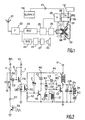
- Figure 1 shows schematically an apparatus image display with a beam screen tube cathodic.
- Figure 2 is a diagram of a device according the invention.
- the invention will be described with reference to a television, but it applies equally well to any display device images, for example to a monitor.
- the television whose diagram is represented on the figure 1 includes a tuner 22 receiving a signal for example of an antenna 21 and transposing its frequency towards intermediate frequencies for a video amplifier 23 and a sound amplifier 24 which follow it.
- the sound intermediate frequency amplifier 24 is followed by a demodulator 29 which delivers the audio signals in baseband to an audio power amplifier 27, powering a speaker 33.
- the frequency amplifier video intermediary 23 is followed by a unit 25 which provides a baseband video signal to a video amplifier 26 delivering ad-hoc signals to the electrodes of a screen tube 32 with cathode beam.
- Unit 25 also extracts signal synchronization signals which are fed to a circuit vertical scanning 28 and a line scanning circuit 36.
- the vertical scanning circuit 28 delivers a current in a frame deflection winding 30.
- the circuit of line sweep is fitted with a line 35 power unit which delivers a current in a deflection coil 34 of line, and produces a voltage called "THT", of about 25 kV, to supply the screen to the screen tube, to which it is connected by a connection 31.
- the power circuit line 35 is powered, via a V1 connection, by a power supply 14, by example of the switching type, connected to the sector.
- Others circuits 22-29 are supplied, as is usual, at from power stage line 35, by connections not shown to simplify the figure.
- a receiver remote control 13 is connected to the line scanning circuit 36 by an RC connection, to control the extinction or the startup, which respectively results in standby or the operation of the parts of the appliance which are supplied by the line 35 power stage.
- the device shown in Figure 2 includes a TP power transistor, here NPN type, which acts way known as winding current switch deflector 34.
- the winding diverter is connected in series with a so-called SC capacitance "of S”, and a recovery diode D1 as well as a CR return capacity are mounted in parallel on the TP power transistor.
- a transformer called “THT” comprises in known manner a primary winding and a plurality of secondary windings. Only the winding primary L1 is shown, which is connected between the collector of the power transistor TP and the terminal power supply V1, the voltage of which is here positive and for example a hundred volts. This voltage is supplied by the mains supply 14 of the figure 1. It is therefore galvanically linked to the sector.
- the end of the L2 + L3 + D2 arrangement i.e. the Ni node, is connected to the base of the power transistor TP by an assembly made of a resistance R3 and a capacity C3 in parallel.
- a resistor R4 is also connected between the point common of inductance L3 and diode D2, on the one hand, and the base of the power transistor TP, on the other hand. If for some reason the blocking of the TP transistor is not ordered in good time, the current continues to increase until desaturation of the transistor TP, at this time the current stops growing, which reduces the voltage in L2, and therefore the base current. The phenomenon is cumulative and the transistor will hang. The blockage is reinforced by the return overvoltage present in L2, which is transmitted to the basis of TP by resistance R4.
- An NPN transistor TB called blocking transistor, which is intended to divert the base current from the transistor of power, so as to block it, connects for this purpose the Ni node to ground.
- Inductance L3 already mentioned is used for limit the current in the transistor TB when the voltage across L2 is positive, although transistor TP either blocked, during the conduction phase of the diode D1.
- a resistor R1 is connected in N2 with the collector of a transistor TC of NPN type, called control transistor, including the emitter supplies a current to the base of the blocking transistor TB, while a resistor 12 between base and emitter of this last facilitates its blocking when the transistor TC is blocked.
- a zener diode Z is connected between the point common N2 and the TB base, of course in such a sense that it does not short-circuit TC in normal operation. In case of failure in the drive control CT, or in the event of a power overvoltage, the voltage would rise in N2 until causing the setting conduction of the diode Z, and consequently the blocking of the TP transistor.
- a capacity connects point N2 to the collector of the transistor TB, that is to say ultimately at the base of the transistor TP, via C3-R3.
- the TC transistor is itself alternately controlled in conduction and blocking, at from a synchronization signal generator circuit line, in a manner to be described later.
- the capacity C1 is partially discharged during conduction transistor TC and transistor TB, which allows then to provide transiently, when the TC and TB transistors block, a current in the base of the power transistor to initiate self-maintenance.
- the control transistor TC is the receiver transistor of an opto-coupler assembly, the emitting diode DE of which is supplied by a transistor TS whose collector is connected by a resistor 7 to a supply V2 which remains present when the device is in standby (this is a voltage which is supplied, in a manner known per se, by a winding isolated from the mains, in the supply 14 of the figure 1).
- the base of the transistor TS is connected by a bias resistor 6 at the voltage source V2, and, via a capacitor C2, to a terminal SY which is an output of a integrated circuit providing a rectangular signal of line synchronization. Resistor 6 has such a value that in the absence of an order via the C2 capacity, the transistor TS is saturated.
- Said integrated circuit is for example a member of the series known as TDA 8360. It contains only several of the elements of FIG. 1 and provides, between others, a line frequency signal. This signal is issued by an open collector output, which is indicated by a TO transistor in the figure.
- An RC terminal carries an on / standby control signal in from the remote control receiver circuit.
- the signal on the RC terminal is for example at +5 volts when the device is on, and goes down to zero volts, when the device is put on standby.
- To the RC terminal is connected a circuit integrator made of a resistance 4 followed by a capacity 8 connected to ground.
- the output of the integrator circuit i.e. the common point of resistance 4 and capacity 8, is connected to output SY by a resistor R2.
- the operation is as follows: in normal operation, the voltage in RC is high, the collector of transistor TO, charged by resistor R2, carries a signal line synchronization, which here is a square wave, and which is transmitted by capacitor C2 at the base of transistor TS. During periods of the square signal where the voltage is low in SY, the capacitor C2 is charged via the resistor 6, and the voltage rises on the base of transistor TS. Values chosen for these elements are such that in operation normal the tension rises almost enough, but not quite does enough to make the TS transistor conductive before the ascent of the square wave in SY. If for some reason any, there was absence of synchronization by TO in due time, this phenomenon would cause the conduction of TS and TP blocking before the current increases there dangerously.
- a reciprocal phenomenon occurs when the tension returns to 5 volts on the RC terminal. Thus are obtained a progressive stop and start of line scanning.
- the resistance 4 and capacitance 8 values allow adjust the duration of the "on” and “off” phases of the transistor TS.
Landscapes
- Engineering & Computer Science (AREA)
- Signal Processing (AREA)
- Multimedia (AREA)
- Theoretical Computer Science (AREA)
- Computer Hardware Design (AREA)
- General Physics & Mathematics (AREA)
- Physics & Mathematics (AREA)
- Remote Sensing (AREA)
- Radar, Positioning & Navigation (AREA)
- Details Of Television Scanning (AREA)
- Dc-Dc Converters (AREA)
- Television Receiver Circuits (AREA)
- Transforming Electric Information Into Light Information (AREA)
Claims (8)
- Bildanzeigegerät, versehen mit einer Bildschirmröhre (32) und einer Vorrichtung, diedadurch gekennzeichnet, daß der besagte Schaltkreis enthält:einen Sägezahnstrom in einer Bildablenkspule (34) erzeugt,mit einem Transformator verschiedene, für das Gerät notwendige Spannungen erzeugt,und, um den Strom der Ablenkspule zu liefern, einen bipolaren Leistungstransistor (TP) enthält, dessen Basisstromüber eine positive Reaktion selbsthaltend ist, bewirkt von einer Wicklung (L2) des Transformators, so in einer Richtung angeschlossen, um der Basis des Leistungstransistors eine geeignete Spannung zu liefern, um dessen Leitfähigkeit zu erhöhen, wenn er bereits leitend ist,und umgeleitet wird, um den Leistungstransistor zu sperren, durch ein Element (TB), dem sogenannten Sperrelement, das abwechselnd leitend gemacht und von einem Zeilenfrequenzsignal gesperrt wird,eine Integratorschaltung (4, 8) aufweist, deren Eingang mit einer Klemme (RC) verbunden ist, die ein Betrieb/Bereitschaft-Signal trägt, und deren Ausgang, der beim Wechsel des Wertes des Betrieb/Bereitschaft-Signals eine progressiv variierende Spannung aufweist, mit einem Schaltkreis verbunden ist, der den Formfaktor des Zeilenfrequenzsignals zur Steuerung des Sperrelements in Übereinstimmung mit der besagten Ausgangsspannung variieren läßt,einen Verstärkertransistor (TO), der an seiner Basis ein Zeilenabtast-Frequenzsignal erhält und mit seinem Kollektor über einen Kollektorwiderstand (R2) mit der besagten progressiv variierenden Spannung verbunden ist,eine Kapazität (C2), die sogenannte zweite Kapazität, und einen Basiswiderstand (6), in Serie zwischen den Kollektor des besagten Verstärkertransistors (TO) und eine Spannungsquelle (V2) geschaltet,einen Steuertransistor (TS), dessen Basis mit dem Mittelpunkt der zweiten Kapazität (C2) und des Basiswiderstands (6) verbunden ist, wobei die leitenden/nichtleitenden Zustände des besagten Steuertransistors (TS) respektive die nichtleitenden/leitenden Zustände des besagten Leistungstransistors (TP) steuern.
- Gerät nach Anspruch 1, dadurch gekennzeichnet, daß, um das Sperrelement zu bilden, der Hauptweg des Stromes eines Transistors, dem sogenannten Sperrtransistor (TB), gesteuert von dem besagten Zeilenfrequenzsignal, zwischen der Basis des Leistungstransistors (TP) und einem Spannungsbezugspunkt liegt.
- Gerät nach Anspruch 2, dadurch gekennzeichnet, daß die Basis des Sperrtransistors (TB) mit dem Emitter eines Transistors verbunden ist, dem sogenannten Steuertransistor (TC), der selbst von einem Zeilenfrequenzsignal gesteuert wird und dessen Kollektor über einen ersten Widerstand (R1) an eine Versorgungsspannungsquelle (V1) angeschlossen ist, wobei eine erste Kapazität (C1) den Kollektor des Steuertransistors (TC) mit der Basis des Leistungstransistors (TP) verbindet.
- Gerät nach Anspruch 3, dadurch gekennzeichnet, daß die Vorrichtung ein optoelektronisches Koppelelement (DE, TC) enthält, dessen empfangender Transistor (TC) den besagten Steuertransistor bildet und dessen Sendediode (DE) von dem besagten Zeilenfrequenzsignal versorgt wird.
- Gerät nach Anspruch 4, dadurch gekennzeichnet, daß die Sendediode (DE) von dem besagten Steuertransistor (TC) versorgt wird, dessen Basis über die besagte Kapazität (C2) mit einer Rechtecksignalquelle zu Zeilenfrequenz verbunden ist und dessen Amplitude entsprechend dem Wert des Betrieb/Bereitschaft-Signals variabel ist.
- Gerät nach Anspruch 1, dadurch gekennzeichnet, daß der Basisstrom des Leistungstransistors (TP) von einer Anordnung geliefert wird, deren eines Ende mit einem Spannungsbezugspunkt verbunden ist, der in Kaskade die besagte Transformatorwicklung (L2), eine Induktanz (L3) und eine Diode (D2) enthält.
- Gerät nach Anspruch 6, dadurch gekennzeichnet, daß das andere Ende der besagten Anordnung mit der Basis des Leistungstransistors (TP) über ein System verbunden ist, das aus einem dritten Transistor (R3) und parallel dazu einer dritten Kapazität (C3) besteht.
- Gerät nach Anspruch 7, dadurch gekennzeichnet, daß eine der Klemmen der Diode (D2) mit dem dritten Widerstand (R3) verbunden, und ein vierter Widerstand (R4) zwischen der anderen Klemme der Diode und der Basis des Leistungstransistors (TP) angeschlossen ist.
Applications Claiming Priority (2)
| Application Number | Priority Date | Filing Date | Title |
|---|---|---|---|
| FR9601479 | 1996-02-07 | ||
| FR9601479A FR2744583A1 (fr) | 1996-02-07 | 1996-02-07 | Appareil d'affichage d'images, muni d'un dispositif de mise en veille progressif |
Publications (2)
| Publication Number | Publication Date |
|---|---|
| EP0789486A1 EP0789486A1 (de) | 1997-08-13 |
| EP0789486B1 true EP0789486B1 (de) | 2001-10-10 |
Family
ID=9488929
Family Applications (1)
| Application Number | Title | Priority Date | Filing Date |
|---|---|---|---|
| EP97200209A Expired - Lifetime EP0789486B1 (de) | 1996-02-07 | 1997-01-27 | Bilderanzeigegerät mit einer progressiven Bereitschaftbetriebsvorrichtung |
Country Status (8)
| Country | Link |
|---|---|
| US (1) | US5796217A (de) |
| EP (1) | EP0789486B1 (de) |
| JP (1) | JPH09238268A (de) |
| KR (1) | KR100427156B1 (de) |
| CN (1) | CN1115863C (de) |
| DE (1) | DE69707166T2 (de) |
| FR (1) | FR2744583A1 (de) |
| MY (1) | MY129734A (de) |
Families Citing this family (3)
| Publication number | Priority date | Publication date | Assignee | Title |
|---|---|---|---|---|
| US7064501B2 (en) * | 2003-02-02 | 2006-06-20 | Jozef Johannes Maria Hulshof | Sawtooth line circuit for a cathode ray tube |
| CN100566376C (zh) * | 2005-12-29 | 2009-12-02 | 康佳集团股份有限公司 | 一种提高阴极射线管电视机高压行扫描输出功率的电路 |
| CN101453170B (zh) * | 2008-12-19 | 2011-06-22 | 深圳创维-Rgb电子有限公司 | 一种分立元器件电源电路 |
Family Cites Families (7)
| Publication number | Priority date | Publication date | Assignee | Title |
|---|---|---|---|---|
| US3793553A (en) * | 1971-08-31 | 1974-02-19 | Gen Electric | Linearity correction circuit using negative feedback |
| FI61256C (fi) * | 1980-08-19 | 1982-06-10 | Salora Oy | Koppling foer linjeslutsteg |
| GB9109595D0 (en) * | 1991-05-02 | 1991-06-26 | Thomson Consumer Electronics | Polling for detection of power supply or other failures of a digital circuit |
| GB9114354D0 (en) * | 1991-07-03 | 1991-08-21 | Thompson Consumer Electronics | Run/standby control with switched mode power supply |
| US5142206A (en) * | 1991-07-15 | 1992-08-25 | Thomson Consumer Electronics, Inc. | Slow turn-on in a deflection circuit |
| JP3393416B2 (ja) * | 1993-09-30 | 2003-04-07 | ソニー株式会社 | 偏平型陰極線管の水平偏向回路 |
| KR0146220B1 (ko) * | 1995-11-06 | 1998-12-01 | 배순훈 | 모니터의 수평 편향회로 |
-
1996
- 1996-02-07 FR FR9601479A patent/FR2744583A1/fr not_active Withdrawn
-
1997
- 1997-01-27 EP EP97200209A patent/EP0789486B1/de not_active Expired - Lifetime
- 1997-01-27 DE DE69707166T patent/DE69707166T2/de not_active Expired - Fee Related
- 1997-02-03 US US08/792,047 patent/US5796217A/en not_active Expired - Fee Related
- 1997-02-04 JP JP9021398A patent/JPH09238268A/ja not_active Abandoned
- 1997-02-05 KR KR1019970003547A patent/KR100427156B1/ko not_active Expired - Fee Related
- 1997-02-06 MY MYPI97000476A patent/MY129734A/en unknown
- 1997-02-07 CN CN97104857A patent/CN1115863C/zh not_active Expired - Fee Related
Also Published As
| Publication number | Publication date |
|---|---|
| KR100427156B1 (ko) | 2004-06-16 |
| CN1115863C (zh) | 2003-07-23 |
| EP0789486A1 (de) | 1997-08-13 |
| FR2744583A1 (fr) | 1997-08-08 |
| MY129734A (en) | 2007-04-30 |
| DE69707166T2 (de) | 2002-06-06 |
| US5796217A (en) | 1998-08-18 |
| DE69707166D1 (de) | 2001-11-15 |
| KR970063016A (ko) | 1997-09-12 |
| CN1168045A (zh) | 1997-12-17 |
| JPH09238268A (ja) | 1997-09-09 |
Similar Documents
| Publication | Publication Date | Title |
|---|---|---|
| EP0041883B1 (de) | Geschaltete Speisespannungseinrichtung mit geregeltem Anschnitt, kombiniert mit der Zeilenablenkschaltung eines Fernsehempfängers, welchen sie speist | |
| EP0789486B1 (de) | Bilderanzeigegerät mit einer progressiven Bereitschaftbetriebsvorrichtung | |
| FR2547474A1 (de) | ||
| US4182978A (en) | Circuit for generating a sawtooth line deflection current | |
| EP0043761B1 (de) | Schalttransistorsteuerschaltung in einem statischen Wandler und Wandler mit dieser Schaltung | |
| US4381477A (en) | Circuit for a picture display device for converting an input d.c. voltage into an output d.c. voltage | |
| EP0022380B1 (de) | Mit einer Zeilenablenkschaltung eines Fernsehempfängers kombinierter Sperrwandler zur Erzeugung einer Betriebsspannung, der mittels variabler Phasenverschiebung geregelt wird | |
| FR2538201A1 (fr) | Regulateur de l'alimentation d'un televiseur repondant aux changements de courant des faisceaux | |
| KR0137274B1 (ko) | 비디오 표시장치의 수직 편향회로 | |
| EP0765076B1 (de) | Horizontalablenkschaltung mit über einen Thyristor eingeschaltetem S-Kondensator | |
| US4238714A (en) | Horizontal deflection output circuit | |
| JPH0511468B2 (de) | ||
| EP0394024B1 (de) | Ablenkantriebsstufe in einem Videogerät | |
| EP0781043B1 (de) | Vorrichtung zur Anzeige von Bildern auf einer Bildschirmröhre, mit einem selbstschwingenden Schaltnetzteil | |
| EP0021915B1 (de) | Vertikalablenkungsschaltung im geschalteten Betrieb für einen Videofrequenzempfänger | |
| EP0055152B1 (de) | Vertikalablenkungsschaltung, Speisung für ihre Steuerung und diese Schaltung umfassender Fernsehempfänger | |
| FR2553612A1 (fr) | Circuit d'interface dans un dispositif de visualisation video, pour le reglage de la frequence de l'oscillateur | |
| KR0137019B1 (ko) | 텔레비젼 편향 장치 | |
| JP3120850B2 (ja) | テレビジョン装置の電源 | |
| US6242863B1 (en) | Spot killer circuit | |
| US5087863A (en) | Feedback arrangement in a deflection circuit | |
| EP0091333B1 (de) | Schutzeinrichtung für die Horizontalablenksteuerung eines Bildschirmes | |
| FR2471102A1 (fr) | Circuit de deviation horizontale commande par le retour du spot | |
| FR2759236A1 (fr) | Base de temps trame pour television | |
| EP0781044A1 (de) | Vorrichtung zur Anzeige von Bildern auf einer Bildschirmröhre |
Legal Events
| Date | Code | Title | Description |
|---|---|---|---|
| PUAI | Public reference made under article 153(3) epc to a published international application that has entered the european phase |
Free format text: ORIGINAL CODE: 0009012 |
|
| AK | Designated contracting states |
Kind code of ref document: A1 Designated state(s): DE ES FR GB IT |
|
| 17P | Request for examination filed |
Effective date: 19980213 |
|
| 17Q | First examination report despatched |
Effective date: 20000117 |
|
| GRAG | Despatch of communication of intention to grant |
Free format text: ORIGINAL CODE: EPIDOS AGRA |
|
| GRAG | Despatch of communication of intention to grant |
Free format text: ORIGINAL CODE: EPIDOS AGRA |
|
| GRAH | Despatch of communication of intention to grant a patent |
Free format text: ORIGINAL CODE: EPIDOS IGRA |
|
| GRAH | Despatch of communication of intention to grant a patent |
Free format text: ORIGINAL CODE: EPIDOS IGRA |
|
| GRAA | (expected) grant |
Free format text: ORIGINAL CODE: 0009210 |
|
| AK | Designated contracting states |
Kind code of ref document: B1 Designated state(s): DE ES FR GB IT |
|
| PG25 | Lapsed in a contracting state [announced via postgrant information from national office to epo] |
Ref country code: IT Free format text: LAPSE BECAUSE OF FAILURE TO SUBMIT A TRANSLATION OF THE DESCRIPTION OR TO PAY THE FEE WITHIN THE PRE;WARNING: LAPSES OF ITALIAN PATENTS WITH EFFECTIVE DATE BEFORE 2007 MAY HAVE OCCURRED AT ANY TIME BEFORE 2007. THE CORRECT EFFECTIVE DATE MAY BE DIFFERENT FROM THE ONE RECORDED.SCRIBED TIME-LIMIT Effective date: 20011010 |
|
| REF | Corresponds to: |
Ref document number: 69707166 Country of ref document: DE Date of ref document: 20011115 |
|
| REG | Reference to a national code |
Ref country code: GB Ref legal event code: IF02 |
|
| GBT | Gb: translation of ep patent filed (gb section 77(6)(a)/1977) |
Effective date: 20011220 |
|
| PG25 | Lapsed in a contracting state [announced via postgrant information from national office to epo] |
Ref country code: ES Free format text: LAPSE BECAUSE OF FAILURE TO SUBMIT A TRANSLATION OF THE DESCRIPTION OR TO PAY THE FEE WITHIN THE PRESCRIBED TIME-LIMIT Effective date: 20020430 |
|
| PLBE | No opposition filed within time limit |
Free format text: ORIGINAL CODE: 0009261 |
|
| STAA | Information on the status of an ep patent application or granted ep patent |
Free format text: STATUS: NO OPPOSITION FILED WITHIN TIME LIMIT |
|
| 26N | No opposition filed | ||
| REG | Reference to a national code |
Ref country code: GB Ref legal event code: 746 Effective date: 20020923 |
|
| REG | Reference to a national code |
Ref country code: FR Ref legal event code: D6 |
|
| PGFP | Annual fee paid to national office [announced via postgrant information from national office to epo] |
Ref country code: GB Payment date: 20050127 Year of fee payment: 9 Ref country code: FR Payment date: 20050127 Year of fee payment: 9 |
|
| PGFP | Annual fee paid to national office [announced via postgrant information from national office to epo] |
Ref country code: DE Payment date: 20050315 Year of fee payment: 9 |
|
| PG25 | Lapsed in a contracting state [announced via postgrant information from national office to epo] |
Ref country code: GB Free format text: LAPSE BECAUSE OF NON-PAYMENT OF DUE FEES Effective date: 20060127 |
|
| PG25 | Lapsed in a contracting state [announced via postgrant information from national office to epo] |
Ref country code: FR Free format text: LAPSE BECAUSE OF NON-PAYMENT OF DUE FEES Effective date: 20060131 |
|
| PG25 | Lapsed in a contracting state [announced via postgrant information from national office to epo] |
Ref country code: DE Free format text: LAPSE BECAUSE OF NON-PAYMENT OF DUE FEES Effective date: 20060801 |
|
| GBPC | Gb: european patent ceased through non-payment of renewal fee |
Effective date: 20060127 |
|
| REG | Reference to a national code |
Ref country code: FR Ref legal event code: ST Effective date: 20060929 |