EP0786911A2 - Spatial light modulator and directional display - Google Patents
Spatial light modulator and directional display Download PDFInfo
- Publication number
- EP0786911A2 EP0786911A2 EP97300481A EP97300481A EP0786911A2 EP 0786911 A2 EP0786911 A2 EP 0786911A2 EP 97300481 A EP97300481 A EP 97300481A EP 97300481 A EP97300481 A EP 97300481A EP 0786911 A2 EP0786911 A2 EP 0786911A2
- Authority
- EP
- European Patent Office
- Prior art keywords
- picture elements
- ith
- jth
- pixels
- picture
- Prior art date
- Legal status (The legal status is an assumption and is not a legal conclusion. Google has not performed a legal analysis and makes no representation as to the accuracy of the status listed.)
- Granted
Links
Images


Classifications
-
- G—PHYSICS
- G02—OPTICS
- G02F—OPTICAL DEVICES OR ARRANGEMENTS FOR THE CONTROL OF LIGHT BY MODIFICATION OF THE OPTICAL PROPERTIES OF THE MEDIA OF THE ELEMENTS INVOLVED THEREIN; NON-LINEAR OPTICS; FREQUENCY-CHANGING OF LIGHT; OPTICAL LOGIC ELEMENTS; OPTICAL ANALOGUE/DIGITAL CONVERTERS
- G02F1/00—Devices or arrangements for the control of the intensity, colour, phase, polarisation or direction of light arriving from an independent light source, e.g. switching, gating or modulating; Non-linear optics
- G02F1/01—Devices or arrangements for the control of the intensity, colour, phase, polarisation or direction of light arriving from an independent light source, e.g. switching, gating or modulating; Non-linear optics for the control of the intensity, phase, polarisation or colour
- G02F1/13—Devices or arrangements for the control of the intensity, colour, phase, polarisation or direction of light arriving from an independent light source, e.g. switching, gating or modulating; Non-linear optics for the control of the intensity, phase, polarisation or colour based on liquid crystals, e.g. single liquid crystal display cells
- G02F1/133—Constructional arrangements; Operation of liquid crystal cells; Circuit arrangements
- G02F1/1333—Constructional arrangements; Manufacturing methods
- G02F1/1335—Structural association of cells with optical devices, e.g. polarisers or reflectors
- G02F1/133509—Filters, e.g. light shielding masks
- G02F1/133514—Colour filters
-
- G—PHYSICS
- G02—OPTICS
- G02B—OPTICAL ELEMENTS, SYSTEMS OR APPARATUS
- G02B30/00—Optical systems or apparatus for producing three-dimensional [3D] effects, e.g. stereoscopic images
- G02B30/20—Optical systems or apparatus for producing three-dimensional [3D] effects, e.g. stereoscopic images by providing first and second parallax images to an observer's left and right eyes
- G02B30/26—Optical systems or apparatus for producing three-dimensional [3D] effects, e.g. stereoscopic images by providing first and second parallax images to an observer's left and right eyes of the autostereoscopic type
- G02B30/27—Optical systems or apparatus for producing three-dimensional [3D] effects, e.g. stereoscopic images by providing first and second parallax images to an observer's left and right eyes of the autostereoscopic type involving lenticular arrays
-
- H—ELECTRICITY
- H04—ELECTRIC COMMUNICATION TECHNIQUE
- H04N—PICTORIAL COMMUNICATION, e.g. TELEVISION
- H04N13/00—Stereoscopic video systems; Multi-view video systems; Details thereof
- H04N13/30—Image reproducers
- H04N13/302—Image reproducers for viewing without the aid of special glasses, i.e. using autostereoscopic displays
- H04N13/31—Image reproducers for viewing without the aid of special glasses, i.e. using autostereoscopic displays using parallax barriers
-
- H—ELECTRICITY
- H04—ELECTRIC COMMUNICATION TECHNIQUE
- H04N—PICTORIAL COMMUNICATION, e.g. TELEVISION
- H04N13/00—Stereoscopic video systems; Multi-view video systems; Details thereof
- H04N13/30—Image reproducers
- H04N13/324—Colour aspects
-
- H—ELECTRICITY
- H04—ELECTRIC COMMUNICATION TECHNIQUE
- H04N—PICTORIAL COMMUNICATION, e.g. TELEVISION
- H04N13/00—Stereoscopic video systems; Multi-view video systems; Details thereof
- H04N13/30—Image reproducers
- H04N13/398—Synchronisation thereof; Control thereof
-
- H—ELECTRICITY
- H04—ELECTRIC COMMUNICATION TECHNIQUE
- H04N—PICTORIAL COMMUNICATION, e.g. TELEVISION
- H04N13/00—Stereoscopic video systems; Multi-view video systems; Details thereof
- H04N13/10—Processing, recording or transmission of stereoscopic or multi-view image signals
- H04N13/189—Recording image signals; Reproducing recorded image signals
-
- H—ELECTRICITY
- H04—ELECTRIC COMMUNICATION TECHNIQUE
- H04N—PICTORIAL COMMUNICATION, e.g. TELEVISION
- H04N13/00—Stereoscopic video systems; Multi-view video systems; Details thereof
- H04N13/10—Processing, recording or transmission of stereoscopic or multi-view image signals
- H04N13/194—Transmission of image signals
-
- H—ELECTRICITY
- H04—ELECTRIC COMMUNICATION TECHNIQUE
- H04N—PICTORIAL COMMUNICATION, e.g. TELEVISION
- H04N13/00—Stereoscopic video systems; Multi-view video systems; Details thereof
- H04N13/20—Image signal generators
- H04N13/204—Image signal generators using stereoscopic image cameras
-
- H—ELECTRICITY
- H04—ELECTRIC COMMUNICATION TECHNIQUE
- H04N—PICTORIAL COMMUNICATION, e.g. TELEVISION
- H04N13/00—Stereoscopic video systems; Multi-view video systems; Details thereof
- H04N13/20—Image signal generators
- H04N13/286—Image signal generators having separate monoscopic and stereoscopic modes
-
- H—ELECTRICITY
- H04—ELECTRIC COMMUNICATION TECHNIQUE
- H04N—PICTORIAL COMMUNICATION, e.g. TELEVISION
- H04N13/00—Stereoscopic video systems; Multi-view video systems; Details thereof
- H04N13/30—Image reproducers
- H04N13/302—Image reproducers for viewing without the aid of special glasses, i.e. using autostereoscopic displays
- H04N13/305—Image reproducers for viewing without the aid of special glasses, i.e. using autostereoscopic displays using lenticular lenses, e.g. arrangements of cylindrical lenses
-
- H—ELECTRICITY
- H04—ELECTRIC COMMUNICATION TECHNIQUE
- H04N—PICTORIAL COMMUNICATION, e.g. TELEVISION
- H04N13/00—Stereoscopic video systems; Multi-view video systems; Details thereof
- H04N13/30—Image reproducers
- H04N13/349—Multi-view displays for displaying three or more geometrical viewpoints without viewer tracking
Definitions
- the present invention relates to a spatial light modulator and to a directional display, such as an autostereoscopic three dimensional (3D) display.
- spatial light modulator as used herein is defined to mean a device which produces as its output light whose intensity can be controlled.
- spatial light modulators include non-emitting devices such as liquid crystal devices (LCD) which modulate light supplied, for instance, from a backlight.
- spatial light modulators also include devices which emit light of controllable intensity, such as electroluminescent devices (ELD).
- ELD electroluminescent devices
- Such spatial light modulators may be used in displays including two dimensional (2D) and 3D displays.
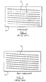
- Figure 1 of the accompanying drawings illustrates a known type of raster scan display such as in conventional television (TV) receivers having cathode ray tubes (CRT) as the display device.
- the video signal standard for conventional TV systems provides two fields which are interlaced to form a video frame.
- the display 1 is of the CRT type and Figure 1 illustrates the raster scan pattern or path on the screen which the electron beam of the CRT follows.
- a first field is illustrated by bold lines such as 2 and contains the odd lines of the image.
- a second field illustrated by lower density lines such as 3 contains the even lines of the image.
- the even lines 3 are interlaced between the odd lines 2 so that the two fields of each frame do not use the same picture elements (pixels) or light emitting regions of the screen of the display 1, i.e. only half of the pixels of the display are addressed in each field.
- This interlaced pattern was introduced in order to reduce display flicker at lower data (field) rates.
- Figure 2 illustrates progressive scanning as used in other known types of displays, such as VGA monitors.
- the lines 4 of each frame are scanned in order (progressively) and the same pixels or regions are scanned by corresponding lines of all frames.
- Figure 3 illustrates the layout of pixels and the colour filtering of an LCD spatial light modulator (SLM) of the type disclosed in EP 0625861.
- the pixels are arranged as rows and columns such that adjacent pairs of columns are contiguous in the direction of the rows.
- the colour filtering comprises horizontal stripes of repeating red, green and blue filters with each stripe covering a single row of pixels.
- FIG. 4 of the accompanying drawings illustrates the use of the SLM 1 of Figure 3 in an autostereoscopic 3D display.
- the SLM is provided with a parallax device 5 illustrated diagrammatically as a lenticular screen comprising parallel lenticules, each of which cooperates with a plurality (three in Figure 4) of pixel columns to generate viewing windows.
- Colour data for each pixel of the image to be displayed are supplied in the form of red, green and blue colour signals RGB to triplets of the SLM pixels.
- Triplets of RGB pixels forming composite colour pixels are indicated by the apices of triangles such as 6 and 7. Arrangements of this type are disclosed in EP 0752610.
- the triangle 6 shown in Figure 3 illustrates the triplet of RGB pixels which constitute the first composite colour pixel of the first line (pixel (1,1)) of the image to be displayed whereas the triangle 7 in Figure 3 forming the first composite colour pixel of the second line (pixel (2,1)).
- the SLM 1 is thus used for progressive scanning without interlacing and this technique may be referred to as 'one phase addressing'.
- each frame comprises a single field.
- the vertical resolution of the image is one third the vertical spatial resolution of the rows of pixels.
- Each pixel of the SLM 1 is addressed only once per frame.
- This type of addressing to form composite colour pixels is particularly necessary for 3D autostereoscopic displays of the type illustrated diagrammatically in Figure 4.
- several images (three in the display of Figure 4) are spatially multiplexed by displaying vertical strips of the three 2D images in the groups of three columns of pixels associated with each parallax element of the parallax device 5.
- the individual pixels of each composite colour pixel must be imaged into the same viewing zone by the parallax device 5.
- the columns of pixels displaying the strips of each 2D image must be in the same horizontal position relative to the corresponding parallax elements.
- the red and blue pixels are in the left hand column behind the parallax element 5a and the green pixel is in the left hand column behind the parallax element 5b so that all three pixels are imaged into the same viewing zone by the parallax device 5.
- a spatial light modulator for displaying M interlaced fields per frame where M is an integer greater than one, characterised by comprising a plurality of picture elements arranged in M different ways as sets of picture elements to form colour picture elements such that substantially all of the picture elements of the spatial light modulator are addressed in each of the M fields.
- a spatial light modulator for displaying M interlaced fields of image data per frame where M is an integer greater than one, comprising a plurality of picture elements and a controller for controlling the supply of the image data to the picture elements such that, in each ith field where i is each integer satisfying 1 ⁇ i ⁇ M, image data are supplied to a plurality of ith sets of picture elements such that each ith set constitutes a composite colour picture element, characterised in that the controller is arranged to control the supply of image data to the picture elements such that, for each jth field where j is each integer satisfying 1 ⁇ j ⁇ M and i ⁇ j, image data are supplied to a plurality of jth sets of picture elements such that each jth set constitutes a composite colour picture element, each ith set is different from each jth set and each ith set has at least one picture element belonging to a jth set.
- each ith and jth set comprises three picture elements disposed at the apices of a triangle and each ith set has two picture elements belonging to a jth set.
- Such an arrangement permits conventional RGB picture elements to be used and maximises the number of picture elements used to display each of the interlaced fields in each addressing phase of the spatial light modulator.
- the modulator may be embodied in LCD technology such that each picture element comprises a liquid crystal picture element.
- the modulator may also be embodied in light emitting technology, such as ELD technology, with each picture element comprising a light emitting element.
- a directional display characterised by comprising a modulator in accordance with the first or second aspect of the invention and a parallax device comprising a plurality of parallax elements, the modulator comprising a plurality of columns of picture elements and each parallax element cooperating with N columns, where N is an integer greater than 1, to produce N viewing zones.
- modulators are applicable to 2D displays, they may also be used in directional displays, for instance of the autostereoscopic 3D type.
- SLMs using conventional addressing techniques for instance as illustrated in Figure 3 and 4
- the present techniques allow at least some of the spatial resolution to be recovered so as to provide a directional display of improved spatial resolution.
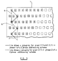
- the SLM 1 shown in Figure 5 has the pixel layout and colour filter arrangement described hereinbefore and shown in Figure 3 but is operated in a two phase addressing scheme to display two interlaced fields per frame of video data.
- the triangles 6 and 7 illustrates triplets of RGB pixels forming composite colour pixels for the first and third lines of the first field in phase 1 of the addressing scheme. These triplets correspond to the single phase addressing scheme illustrated in Figure 3.
- a triangle 8 shown in broken lines illustrates a triplet of RGB pixels forming a composite colour pixel at the beginning of the second image line which is the first image line of the second field addressed in the second phase of the addressing scheme.
- the green and blue pixels at the apices of the triangle 8 are the green and blue pixels at the apices of the triangle 6 used during the first phase of the two phase addressing scheme.
- the red pixel is not the same in the two phases.
- the large numerals '1' and '2' within the triangles indicate which groups of pixels are used to form the composite colour pixels in the first and second fields addressed during the first and second phases, respectively, of the two phase addressing scheme. For instance, pixels 10, 11 and 12 are grouped to provide a single composite colour pixel during the first field whereas the pixels 11 and 12 are grouped with a pixel 13 to form a composite colour pixel of the second field. Apart from the top and bottom rows of pixels, all of the pixels are addressed in each of the first and second fields but the centroids of the colour pixels in the second field are shifted vertically downwardly by one row with respect to the colour pixels addressed in the first field.
- This addressing scheme provides improved compatibility with interlaced 3D image signals, for instance where each 2D image is sourced from an interlaced television signal.
- each 2D image is sourced from an interlaced television signal.
- substantially every line of the SLM is addressed in every phase.
- the period between addressing phases is preferably less than 0.05 seconds and more preferably less than 0.005 seconds.
- Each of the pixels, such as 11, 12, and 13, addressed in both the first and second phases will (in general) be addressed with different image values giving rise to different intensities if the SLM 1 is of the "fast" response type.
- a "fast” SLM is one in which the maximum optical response time to achieve any optical level e.g. a "black” level, a "white” level or any intermediate “grey” level, from any other optical level is less than or equal to the period between the start of consecutive addressing phases.
- each pixel displays an R.M.S. average of the optical levels demanded by the pixel signals in consecutive addressing phases. This improves the visual perception of the display, particularly when the display is of low resolution. For instance, in the case of a nine inch display panel viewed from 0.5 metres, "low resolution" would generally mean an array of pixels comprising less than 640 by 480 pixels.
- Fractional (such as one half or one third) resolution is a consequence of multi-view 3D displays where the pixels of the SLM must be shared among the actual views. For example, a 2D display comprising three million pixels will, when used as a three view 3D display, normally only have a resolution of one million pixels in each of the views.
- the techniques described herein provide a substantial improvement in the image quality of such autostereoscopic displays. Furthermore, as will be clear to those skilled in the art, the techniques described herein reduce the visibility of the well-known jagged or "stair-strip" line effect which is often seen when conventional displays try to display straight lines at small angles to the horizontal.
- a device of this type has actually been implemented in the form of a 9 inch (approximately 22.5 centimetre) TFT colour LCD.
- two fields of different information each with the same resolution as the SLM, can be displayed with superior perceived image quality compared with repetitively displaying one field alone or displaying the two fields of data directly on top of each other i.e. with no spatial offset.
- FIG. 7 illustrates a three phase addressing scheme in which each frame of video data comprises three interlaced fields.
- the RGB triplets at the apices of the triangles 6 and 7 represent the first composite colour pixels in consecutive lines of the first field addressed in the first phase.
- the composite pixel illustrated by the triangle 7 is now the first composite colour pixel of the fourth line of the image.
- the RGB pixel triplet indicated by the apices of the triangle 8 again comprises the first pixel of the first line of the second field addressed in the second phase and constitutes the first composite pixel of the second line of the frame.
- the first composite pixel of the third field addressed during the third phase is indicated by the RGB pixels at the apices of a triangle 9.
- This composite pixel constitutes the first pixel of the third row of the frame.
- all of the rows of pixels except two are addressed in all three phases of the three phase addressing scheme. For instance, an image comprising 480 lines can be divided into three interleaved 160 line images which may then be displayed by the SLM 1 having 162 lines. The visual resolution is thus effectively tripled.
- Figure 8 illustrates the use of the three phase addressing scheme in an autostereoscopic 3D display.
- the large numerals '1', '2' and '3' within the triangles again represent the triplets of pixels forming composite pixels during the first, second and third phases, respectively, of the three phase addressing scheme.
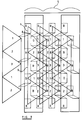
- FIG 9 is a block schematic diagram of an SLM for multiphase addressing as illustrated in Figures 5 to 8.
- the SLM comprises an array 20 of pixels arranged as rows and columns as illustrated, for instance, in Figure 5, connected to a controller for controlling addressing of the pixels.
- the controller comprises an address generator 21 having a respective output 21a connected to each row electrode which is connected to all the pixels of the respective row.
- a driver 22 has a respective output 22a for each column electrode connected to all of the pixels of a respective column.
- the driver 22 has inputs which correspond to its outputs and which are connected to the respective outputs 23a of a latch 23.
- the latch 23 similarly has inputs which correspond to its outputs and which are connected to respective outputs 24a of a serial in/parallel out shift register 24.
- the shift register 24 has a data input connected to the output 25a of a data ordering circuit 25 for supplying video signals in the appropriate serial format for the multiphase addressing described hereinbefore.
- a timing generator 26 is connected to the output 25a of the circuit 25 and converts timing signals from the video input signal to timing signals for controlling the SLM.
- the timing generator 26 has a first output 26a connected to a clock input of the shift register for clocking (or sampling) each video line of data serially.
- a second output 26b of the timing generator 26 is connected to a latch enable input of the latch 23 for enabling the latch 23 to store a next line of display data.
- a third output 26c of the timing generator 26 is connected to the driver 22 so as to enable the supply of the row of data to the column electrodes of the array 20.
- the timing generator 26 has a fourth output 27 which controls the timing of the supply by the address generator 21 of strobe signals to the row electrodes of the array 20.
- the address generator 21 supplies one strobe signal at a time at its outputs so as to strobe one line of video data at a time into the array 20 of pixels.
- the address generator supplies strobe signals during the first phase in turn one row at a time to the rows of the array 20.
- the addressing generator again supplies strobe signals in sequence one row at a time to the rows of the array 20, for instance from the top to the bottom of the array 20, so as to supply the second phase of video data to the array.
- the data ordering circuit 25 is shown as having an input 28, for instance for a standard video signal carrying two field interlaced image data.
- the circuit 25 may comprise a computer and/or frame store arranged to convert the incoming video signal into two or three field interlaced image data ordered correctly for two or three phase addressing into the array 20.
- the circuit 25 may be embodied as an application specific integrated circuit ASIC.
- the circuit may be arranged to reorder video data of other formats, which may be interlaced or non-interlaced.
- the circuit 25 forms part of a video source, such as a personal computer (PC), which is arranged to generate image data which are in the correct format for multiphase addressing into the array 20.
- a video source such as a personal computer (PC)
- PC personal computer
- the address generator 21 supplies the strobe pulses in turn one row at a time to the rows of the array 20 during the first phase.
- the address generator 21 supplies the strobe signals in turn one row at a time to the rows of the array 20 during the second phase.
- the address generator 21 supplies the strobe signals in turn one row at a time to the rows of the array 20.
- the SLM may employ active or passive matrix addressing with the multiphase addressing scheme described hereinbefore.
- the array 20 may comprise light valve (non-light-emitting) or light-emitting pixels.
- the array may be embodied as a liquid crystal device whereas, for the light-emitting case, the array 20 may be embodied as an electroluminescent device.
- FIG. 8 illustrate SLM's having a horizontally striped colour filter pattern with the RGB pixel triplets at the apices of triangles
- the SLMs are not limited to such arrangements.
- Other colour filter patterning and other RGB triplet patterns could equally well be used, such as those disclosed in Figures 18, 19 and 20 EP 0752610.
- such SLMs are not limited to RGB triplets but other sets, such quadruplets (for instance RGGB or RGYB where Y is a 'white' pixel) whose pixels are at the apices of quadrilaterals, could be used.
Landscapes
- Physics & Mathematics (AREA)
- Engineering & Computer Science (AREA)
- Multimedia (AREA)
- Signal Processing (AREA)
- Nonlinear Science (AREA)
- Optics & Photonics (AREA)
- General Physics & Mathematics (AREA)
- Mathematical Physics (AREA)
- Chemical & Material Sciences (AREA)
- Crystallography & Structural Chemistry (AREA)
- Control Of Indicators Other Than Cathode Ray Tubes (AREA)
- Liquid Crystal (AREA)
- Testing, Inspecting, Measuring Of Stereoscopic Televisions And Televisions (AREA)
Abstract

Description
- The present invention relates to a spatial light modulator and to a directional display, such as an autostereoscopic three dimensional (3D) display.
- The term 'spatial light modulator' as used herein is defined to mean a device which produces as its output light whose intensity can be controlled. Thus, spatial light modulators include non-emitting devices such as liquid crystal devices (LCD) which modulate light supplied, for instance, from a backlight. However, spatial light modulators also include devices which emit light of controllable intensity, such as electroluminescent devices (ELD). Such spatial light modulators may be used in displays including two dimensional (2D) and 3D displays.
- Figure 1 of the accompanying drawings illustrates a known type of raster scan display such as in conventional television (TV) receivers having cathode ray tubes (CRT) as the display device. The video signal standard for conventional TV systems provides two fields which are interlaced to form a video frame. The
display 1 is of the CRT type and Figure 1 illustrates the raster scan pattern or path on the screen which the electron beam of the CRT follows. A first field is illustrated by bold lines such as 2 and contains the odd lines of the image. A second field illustrated by lower density lines such as 3 contains the even lines of the image. As shown in Figure 1, theeven lines 3 are interlaced between theodd lines 2 so that the two fields of each frame do not use the same picture elements (pixels) or light emitting regions of the screen of thedisplay 1, i.e. only half of the pixels of the display are addressed in each field. - This interlaced pattern was introduced in order to reduce display flicker at lower data (field) rates.
- Figure 2 illustrates progressive scanning as used in other known types of displays, such as VGA monitors. In this case, the lines 4 of each frame are scanned in order (progressively) and the same pixels or regions are scanned by corresponding lines of all frames.
- Figure 3 illustrates the layout of pixels and the colour filtering of an LCD spatial light modulator (SLM) of the type disclosed in EP 0625861. The pixels are arranged as rows and columns such that adjacent pairs of columns are contiguous in the direction of the rows. The colour filtering comprises horizontal stripes of repeating red, green and blue filters with each stripe covering a single row of pixels.
- Figure 4 of the accompanying drawings illustrates the use of the
SLM 1 of Figure 3 in an autostereoscopic 3D display. The SLM is provided with aparallax device 5 illustrated diagrammatically as a lenticular screen comprising parallel lenticules, each of which cooperates with a plurality (three in Figure 4) of pixel columns to generate viewing windows. - Colour data for each pixel of the image to be displayed are supplied in the form of red, green and blue colour signals RGB to triplets of the SLM pixels. Triplets of RGB pixels forming composite colour pixels are indicated by the apices of triangles such as 6 and 7. Arrangements of this type are disclosed in EP 0752610. Thus, the
triangle 6 shown in Figure 3 illustrates the triplet of RGB pixels which constitute the first composite colour pixel of the first line (pixel (1,1)) of the image to be displayed whereas thetriangle 7 in Figure 3 forming the first composite colour pixel of the second line (pixel (2,1)). TheSLM 1 is thus used for progressive scanning without interlacing and this technique may be referred to as 'one phase addressing'. This is indicated in Figure 4 by the large numeral '1' appearing in thetriangles - This type of addressing to form composite colour pixels is particularly necessary for 3D autostereoscopic displays of the type illustrated diagrammatically in Figure 4. In such a display, several images (three in the display of Figure 4) are spatially multiplexed by displaying vertical strips of the three 2D images in the groups of three columns of pixels associated with each parallax element of the
parallax device 5. In order to create an autostereoscopic full-colour image, the individual pixels of each composite colour pixel must be imaged into the same viewing zone by theparallax device 5. Thus, the columns of pixels displaying the strips of each 2D image must be in the same horizontal position relative to the corresponding parallax elements. For example, as indicated by thetriangle 6 in Figure 4, the red and blue pixels are in the left hand column behind the parallax element 5a and the green pixel is in the left hand column behind the parallax element 5b so that all three pixels are imaged into the same viewing zone by theparallax device 5. - Although it is theoretically possible to increase the vertical resolution of a display using an
SLM 1 addressed as shown in Figures 3 and 4, there are practical difficulties. For instance, if the pixels of theSLM 1 are made to the current practical limits of spatial resolution, no further increase in resolution is possible. Also, increasing the vertical resolution by increasing the number of addressed rows can have a disadvantageous effect on display brightness or contrast. In the case of passive matrix displays, increasing the number of addressed rows directly reduces the display contrast. - According to a first aspect of the invention, there is provided a spatial light modulator for displaying M interlaced fields per frame where M is an integer greater than one, characterised by comprising a plurality of picture elements arranged in M different ways as sets of picture elements to form colour picture elements such that substantially all of the picture elements of the spatial light modulator are addressed in each of the M fields.
- According to a second aspect of the invention, there is provided a spatial light modulator for displaying M interlaced fields of image data per frame where M is an integer greater than one, comprising a plurality of picture elements and a controller for controlling the supply of the image data to the picture elements such that, in each ith field where i is each integer satisfying 1 ≤ i ≤ M, image data are supplied to a plurality of ith sets of picture elements such that each ith set constitutes a composite colour picture element, characterised in that the controller is arranged to control the supply of image data to the picture elements such that, for each jth field where j is each integer satisfying 1 ≤ j ≤ M and i ≠ j, image data are supplied to a plurality of jth sets of picture elements such that each jth set constitutes a composite colour picture element, each ith set is different from each jth set and each ith set has at least one picture element belonging to a jth set.
- It is thus possible to provide a spatial light modulator whose vertical resolution is effectively increased without increasing the number of picture elements. Most of the picture elements are used in each of the fields or addressing phases so that the perceived vertical resolution is greater than, for instance, the arrangement illustrated in Figures 3 and 4. In particular, it is possible to arrange addressing such that only (M-1) rows of picture elements are not used to display all of the M fields. The improved resolution may be achieved with little or no penalty in terms of manufacturing difficulty or cost.
- Preferably each ith and jth set comprises three picture elements disposed at the apices of a triangle and each ith set has two picture elements belonging to a jth set. Such an arrangement permits conventional RGB picture elements to be used and maximises the number of picture elements used to display each of the interlaced fields in each addressing phase of the spatial light modulator.
- The modulator may be embodied in LCD technology such that each picture element comprises a liquid crystal picture element. However, the modulator may also be embodied in light emitting technology, such as ELD technology, with each picture element comprising a light emitting element.
- According to a third aspect of the invention, there is provided a directional display characterised by comprising a modulator in accordance with the first or second aspect of the invention and a parallax device comprising a plurality of parallax elements, the modulator comprising a plurality of columns of picture elements and each parallax element cooperating with N columns, where N is an integer greater than 1, to produce N viewing zones.
- Although such modulators are applicable to 2D displays, they may also be used in directional displays, for instance of the autostereoscopic 3D type. When SLMs using conventional addressing techniques, for instance as illustrated in Figure 3 and 4, are used in directional displays, there is an inevitable loss of spatial resolution compared with the use of such SLMs as 2D displays. The present techniques allow at least some of the spatial resolution to be recovered so as to provide a directional display of improved spatial resolution.
- The invention will be further described, way of example, with reference to the accompanying drawings, in which:
- Figures 1 and 2 are diagrams illustrated known interlaced and non-interlaced raster scanning techniques, respectively;
- Figure 3 illustrates use of an SLM for conventional single phase addressing;
- Figure 4 illustrates diagrammatically the use of an SLM of the type illustrated in Figure 3 as part of an autostereoscopic 3D display;
- Figure 5 illustrates an SLM using a two phase addressing scheme to provide an embodiment of the invention;
- Figure 6 illustrates the use of the SLM of Figure 5 in an autostereoscopic 3D display;
- Figure 7 illustrates an SLM operating in a three phase addressing scheme to provide another embodiment of the invention;
- Figure 8 illustrates the use of the SLM of Figure 7 in an autostereoscopic 3D display; and
- Figure 9 is a block schematic diagram of an SLM of the type shown in Figures 5 to 7.
- Like reference numerals refer to like parts throughout the drawings.
- The
SLM 1 shown in Figure 5 has the pixel layout and colour filter arrangement described hereinbefore and shown in Figure 3 but is operated in a two phase addressing scheme to display two interlaced fields per frame of video data. Thetriangles phase 1 of the addressing scheme. These triplets correspond to the single phase addressing scheme illustrated in Figure 3. - A
triangle 8 shown in broken lines illustrates a triplet of RGB pixels forming a composite colour pixel at the beginning of the second image line which is the first image line of the second field addressed in the second phase of the addressing scheme. Thus, in the second addressing phase, the green and blue pixels at the apices of thetriangle 8 are the green and blue pixels at the apices of thetriangle 6 used during the first phase of the two phase addressing scheme. The red pixel is not the same in the two phases. - As shown in Figure 6, the large numerals '1' and '2' within the triangles indicate which groups of pixels are used to form the composite colour pixels in the first and second fields addressed during the first and second phases, respectively, of the two phase addressing scheme. For instance,
pixels pixels - In order to avoid image jerkiness and/or flicker, the period between addressing phases is preferably less than 0.05 seconds and more preferably less than 0.005 seconds. Each of the pixels, such as 11, 12, and 13, addressed in both the first and second phases will (in general) be addressed with different image values giving rise to different intensities if the
SLM 1 is of the "fast" response type. A "fast" SLM is one in which the maximum optical response time to achieve any optical level e.g. a "black" level, a "white" level or any intermediate "grey" level, from any other optical level is less than or equal to the period between the start of consecutive addressing phases. However, where the response time is greater than this, for instance as is the case for the twisted nematic liquid crystal (TN LC) effect commonly used in SLMs, each pixel displays an R.M.S. average of the optical levels demanded by the pixel signals in consecutive addressing phases. This improves the visual perception of the display, particularly when the display is of low resolution. For instance, in the case of a nine inch display panel viewed from 0.5 metres, "low resolution" would generally mean an array of pixels comprising less than 640 by 480 pixels. - Fractional (such as one half or one third) resolution is a consequence of multi-view 3D displays where the pixels of the SLM must be shared among the actual views. For example, a 2D display comprising three million pixels will, when used as a three view 3D display, normally only have a resolution of one million pixels in each of the views. The techniques described herein provide a substantial improvement in the image quality of such autostereoscopic displays. Furthermore, as will be clear to those skilled in the art, the techniques described herein reduce the visibility of the well-known jagged or "stair-strip" line effect which is often seen when conventional displays try to display straight lines at small angles to the horizontal.
- A device of this type has actually been implemented in the form of a 9 inch (approximately 22.5 centimetre) TFT colour LCD.
- Thus, two fields of different information, each with the same resolution as the SLM, can be displayed with superior perceived image quality compared with repetitively displaying one field alone or displaying the two fields of data directly on top of each other i.e. with no spatial offset.
- Figure 7 illustrates a three phase addressing scheme in which each frame of video data comprises three interlaced fields. As in the arrangement illustrated in Figure 5, the RGB triplets at the apices of the
triangles triangle 7 is now the first composite colour pixel of the fourth line of the image. The RGB pixel triplet indicated by the apices of thetriangle 8 again comprises the first pixel of the first line of the second field addressed in the second phase and constitutes the first composite pixel of the second line of the frame. - The first composite pixel of the third field addressed during the third phase is indicated by the RGB pixels at the apices of a
triangle 9. This composite pixel constitutes the first pixel of the third row of the frame. In this case, all of the rows of pixels except two are addressed in all three phases of the three phase addressing scheme. For instance, an image comprising 480 lines can be divided into three interleaved 160 line images which may then be displayed by theSLM 1 having 162 lines. The visual resolution is thus effectively tripled. - Figure 8 illustrates the use of the three phase addressing scheme in an autostereoscopic 3D display. The large numerals '1', '2' and '3' within the triangles again represent the triplets of pixels forming composite pixels during the first, second and third phases, respectively, of the three phase addressing scheme.
- Figure 9 is a block schematic diagram of an SLM for multiphase addressing as illustrated in Figures 5 to 8. The SLM comprises an
array 20 of pixels arranged as rows and columns as illustrated, for instance, in Figure 5, connected to a controller for controlling addressing of the pixels. The controller comprises anaddress generator 21 having a respective output 21a connected to each row electrode which is connected to all the pixels of the respective row. Similarly, adriver 22 has a respective output 22a for each column electrode connected to all of the pixels of a respective column. Thedriver 22 has inputs which correspond to its outputs and which are connected to the respective outputs 23a of alatch 23. Thelatch 23 similarly has inputs which correspond to its outputs and which are connected to respective outputs 24a of a serial in/parallelout shift register 24. Theshift register 24 has a data input connected to the output 25a of adata ordering circuit 25 for supplying video signals in the appropriate serial format for the multiphase addressing described hereinbefore. - A
timing generator 26 is connected to the output 25a of thecircuit 25 and converts timing signals from the video input signal to timing signals for controlling the SLM. Thetiming generator 26 has a first output 26a connected to a clock input of the shift register for clocking (or sampling) each video line of data serially. A second output 26b of thetiming generator 26 is connected to a latch enable input of thelatch 23 for enabling thelatch 23 to store a next line of display data. A third output 26c of thetiming generator 26 is connected to thedriver 22 so as to enable the supply of the row of data to the column electrodes of thearray 20. Thetiming generator 26 has afourth output 27 which controls the timing of the supply by theaddress generator 21 of strobe signals to the row electrodes of thearray 20. - The
address generator 21 supplies one strobe signal at a time at its outputs so as to strobe one line of video data at a time into thearray 20 of pixels. In the case of a two phase addressing scheme as illustrated in Figures 5 and 6, the address generator supplies strobe signals during the first phase in turn one row at a time to the rows of thearray 20. When strobing of the first phase data into thearray 20 is complete, the addressing generator again supplies strobe signals in sequence one row at a time to the rows of thearray 20, for instance from the top to the bottom of thearray 20, so as to supply the second phase of video data to the array. - The
data ordering circuit 25 is shown as having aninput 28, for instance for a standard video signal carrying two field interlaced image data. Thecircuit 25 may comprise a computer and/or frame store arranged to convert the incoming video signal into two or three field interlaced image data ordered correctly for two or three phase addressing into thearray 20. Thecircuit 25 may be embodied as an application specific integrated circuit ASIC. The circuit may be arranged to reorder video data of other formats, which may be interlaced or non-interlaced. - In another arrangement, the
circuit 25 forms part of a video source, such as a personal computer (PC), which is arranged to generate image data which are in the correct format for multiphase addressing into thearray 20. - In the case of a three phase addressing scheme as illustrated in Figures 7 and 8, the
address generator 21 supplies the strobe pulses in turn one row at a time to the rows of thearray 20 during the first phase. Theaddress generator 21 supplies the strobe signals in turn one row at a time to the rows of thearray 20 during the second phase. During the third phase, theaddress generator 21 supplies the strobe signals in turn one row at a time to the rows of thearray 20. - The SLM may employ active or passive matrix addressing with the multiphase addressing scheme described hereinbefore. Further, the
array 20 may comprise light valve (non-light-emitting) or light-emitting pixels. For the light valve case, the array may be embodied as a liquid crystal device whereas, for the light-emitting case, thearray 20 may be embodied as an electroluminescent device. - Although Figure 5 to 8 illustrate SLM's having a horizontally striped colour filter pattern with the RGB pixel triplets at the apices of triangles, the SLMs are not limited to such arrangements. Other colour filter patterning and other RGB triplet patterns could equally well be used, such as those disclosed in Figures 18, 19 and 20 EP 0752610. Also, such SLMs are not limited to RGB triplets but other sets, such quadruplets (for instance RGGB or RGYB where Y is a 'white' pixel) whose pixels are at the apices of quadrilaterals, could be used.
Claims (6)
- A spatial light modulator for displaying M interlaced fields per frame where M is an integer greater than one, characterised by comprising a plurality of picture elements (20) arranged in M different ways as sets of picture elements to form colour picture elements such that substantially all of the picture elements of the spatial light modulator are addressed in each of the M fields.
- A spatial light modulator for displaying M interlaced fields of image data per frame where M is an integer greater than one, comprising a plurality of picture elements (20) and a controller (21-28) for controlling the supply of the image data to the picture elements (20) such that, in each ith field where i is each integer satisfying 1 ≤ i ≤ M, image data are supplied to a plurality of ith sets of picture elements (10, 11, 12) such that each ith set constitutes a composite colour picture element, characterised in that the controller is arranged to control the supply of image data to the picture elements such that, for each jth field where j is each integer satisfying 1 ≤ j ≤ M and i ≠ j, image data are supplied to a plurality of jth sets of picture elements (11, 12, 13) such that each jth set constitutes a composite colour picture element, each ith set is different from each jth set, and each ith set has at least one picture element (11, 12) belonging to a jth set.
- A modulator as claimed in Claim 2, characterised in that each ith and jth set comprises three picture elements (10, 11, 12; 11, 12, 13) disposed at the apices of a triangle and each ith set has two picture elements (11, 12) belonging to a jth set.
- A modulator as claimed in Claim 2 or Claim 3, characterised in that each picture element comprises a liquid crystal picture element.
- A modulator as claimed in Claim 2 or Claim 3, characterised in that each picture element comprises a light emitting element.
- A directional display characterised by comprising a modulator (20-28) as claimed in any one of the preceding claims and a parallax device (5) comprising a plurality of parallax elements (5a, 5b), the modulator comprising a plurality of columns of picture elements and each parallax element (5a, 5b) cooperating with N columns, where N is an integer greater than one, to produce N viewing zones.
Priority Applications (1)
| Application Number | Priority Date | Filing Date | Title |
|---|---|---|---|
| EP97300481A EP0786911B1 (en) | 1996-01-26 | 1997-01-27 | Autostereoscopic display |
Applications Claiming Priority (3)
| Application Number | Priority Date | Filing Date | Title |
|---|---|---|---|
| GB9601618 | 1996-01-26 | ||
| GB9601618A GB2309572A (en) | 1996-01-26 | 1996-01-26 | Spatial light modulator display |
| EP97300481A EP0786911B1 (en) | 1996-01-26 | 1997-01-27 | Autostereoscopic display |
Publications (3)
| Publication Number | Publication Date |
|---|---|
| EP0786911A2 true EP0786911A2 (en) | 1997-07-30 |
| EP0786911A3 EP0786911A3 (en) | 1998-07-01 |
| EP0786911B1 EP0786911B1 (en) | 2003-09-10 |
Family
ID=26147274
Family Applications (1)
| Application Number | Title | Priority Date | Filing Date |
|---|---|---|---|
| EP97300481A Expired - Lifetime EP0786911B1 (en) | 1996-01-26 | 1997-01-27 | Autostereoscopic display |
Country Status (1)
| Country | Link |
|---|---|
| EP (1) | EP0786911B1 (en) |
Cited By (13)
| Publication number | Priority date | Publication date | Assignee | Title |
|---|---|---|---|---|
| US7525730B2 (en) | 2004-09-27 | 2009-04-28 | Idc, Llc | Method and device for generating white in an interferometric modulator display |
| US7706050B2 (en) | 2004-03-05 | 2010-04-27 | Qualcomm Mems Technologies, Inc. | Integrated modulator illumination |
| US7813026B2 (en) | 2004-09-27 | 2010-10-12 | Qualcomm Mems Technologies, Inc. | System and method of reducing color shift in a display |
| US8040588B2 (en) | 2004-09-27 | 2011-10-18 | Qualcomm Mems Technologies, Inc. | System and method of illuminating interferometric modulators using backlighting |
| US8798425B2 (en) | 2007-12-07 | 2014-08-05 | Qualcomm Mems Technologies, Inc. | Decoupled holographic film and diffuser |
| US8848294B2 (en) | 2010-05-20 | 2014-09-30 | Qualcomm Mems Technologies, Inc. | Method and structure capable of changing color saturation |
| US8872085B2 (en) | 2006-10-06 | 2014-10-28 | Qualcomm Mems Technologies, Inc. | Display device having front illuminator with turning features |
| US8928967B2 (en) | 1998-04-08 | 2015-01-06 | Qualcomm Mems Technologies, Inc. | Method and device for modulating light |
| US8971675B2 (en) | 2006-01-13 | 2015-03-03 | Qualcomm Mems Technologies, Inc. | Interconnect structure for MEMS device |
| US9019183B2 (en) | 2006-10-06 | 2015-04-28 | Qualcomm Mems Technologies, Inc. | Optical loss structure integrated in an illumination apparatus |
| US9019590B2 (en) | 2004-02-03 | 2015-04-28 | Qualcomm Mems Technologies, Inc. | Spatial light modulator with integrated optical compensation structure |
| US9025235B2 (en) | 2002-12-25 | 2015-05-05 | Qualcomm Mems Technologies, Inc. | Optical interference type of color display having optical diffusion layer between substrate and electrode |
| US9110289B2 (en) | 1998-04-08 | 2015-08-18 | Qualcomm Mems Technologies, Inc. | Device for modulating light with multiple electrodes |
Families Citing this family (15)
| Publication number | Priority date | Publication date | Assignee | Title |
|---|---|---|---|---|
| US7907319B2 (en) | 1995-11-06 | 2011-03-15 | Qualcomm Mems Technologies, Inc. | Method and device for modulating light with optical compensation |
| WO2003007049A1 (en) | 1999-10-05 | 2003-01-23 | Iridigm Display Corporation | Photonic mems and structures |
| US7855824B2 (en) | 2004-03-06 | 2010-12-21 | Qualcomm Mems Technologies, Inc. | Method and system for color optimization in a display |
| US8031133B2 (en) | 2004-09-27 | 2011-10-04 | Qualcomm Mems Technologies, Inc. | Method and device for manipulating color in a display |
| US8102407B2 (en) | 2004-09-27 | 2012-01-24 | Qualcomm Mems Technologies, Inc. | Method and device for manipulating color in a display |
| US7898521B2 (en) | 2004-09-27 | 2011-03-01 | Qualcomm Mems Technologies, Inc. | Device and method for wavelength filtering |
| US8362987B2 (en) | 2004-09-27 | 2013-01-29 | Qualcomm Mems Technologies, Inc. | Method and device for manipulating color in a display |
| US7911428B2 (en) | 2004-09-27 | 2011-03-22 | Qualcomm Mems Technologies, Inc. | Method and device for manipulating color in a display |
| US8004504B2 (en) | 2004-09-27 | 2011-08-23 | Qualcomm Mems Technologies, Inc. | Reduced capacitance display element |
| US7710632B2 (en) | 2004-09-27 | 2010-05-04 | Qualcomm Mems Technologies, Inc. | Display device having an array of spatial light modulators with integrated color filters |
| US7928928B2 (en) | 2004-09-27 | 2011-04-19 | Qualcomm Mems Technologies, Inc. | Apparatus and method for reducing perceived color shift |
| US7807488B2 (en) | 2004-09-27 | 2010-10-05 | Qualcomm Mems Technologies, Inc. | Display element having filter material diffused in a substrate of the display element |
| US7710636B2 (en) | 2004-09-27 | 2010-05-04 | Qualcomm Mems Technologies, Inc. | Systems and methods using interferometric optical modulators and diffusers |
| US8004743B2 (en) | 2006-04-21 | 2011-08-23 | Qualcomm Mems Technologies, Inc. | Method and apparatus for providing brightness control in an interferometric modulator (IMOD) display |
| US8072402B2 (en) | 2007-08-29 | 2011-12-06 | Qualcomm Mems Technologies, Inc. | Interferometric optical modulator with broadband reflection characteristics |
Citations (3)
| Publication number | Priority date | Publication date | Assignee | Title |
|---|---|---|---|---|
| EP0244013A1 (en) * | 1986-04-25 | 1987-11-04 | Koninklijke Philips Electronics N.V. | Colour display device |
| EP0454538A1 (en) * | 1990-04-27 | 1991-10-30 | Thomson-Lcd | Colour matrix display with interlaced addressing |
| EP0625861A2 (en) * | 1993-05-21 | 1994-11-23 | Sharp Kabushiki Kaisha | Spatial light modulator and directional display |
-
1997
- 1997-01-27 EP EP97300481A patent/EP0786911B1/en not_active Expired - Lifetime
Patent Citations (3)
| Publication number | Priority date | Publication date | Assignee | Title |
|---|---|---|---|---|
| EP0244013A1 (en) * | 1986-04-25 | 1987-11-04 | Koninklijke Philips Electronics N.V. | Colour display device |
| EP0454538A1 (en) * | 1990-04-27 | 1991-10-30 | Thomson-Lcd | Colour matrix display with interlaced addressing |
| EP0625861A2 (en) * | 1993-05-21 | 1994-11-23 | Sharp Kabushiki Kaisha | Spatial light modulator and directional display |
Cited By (15)
| Publication number | Priority date | Publication date | Assignee | Title |
|---|---|---|---|---|
| US8928967B2 (en) | 1998-04-08 | 2015-01-06 | Qualcomm Mems Technologies, Inc. | Method and device for modulating light |
| US9110289B2 (en) | 1998-04-08 | 2015-08-18 | Qualcomm Mems Technologies, Inc. | Device for modulating light with multiple electrodes |
| US9025235B2 (en) | 2002-12-25 | 2015-05-05 | Qualcomm Mems Technologies, Inc. | Optical interference type of color display having optical diffusion layer between substrate and electrode |
| US9019590B2 (en) | 2004-02-03 | 2015-04-28 | Qualcomm Mems Technologies, Inc. | Spatial light modulator with integrated optical compensation structure |
| US7880954B2 (en) | 2004-03-05 | 2011-02-01 | Qualcomm Mems Technologies, Inc. | Integrated modulator illumination |
| US7706050B2 (en) | 2004-03-05 | 2010-04-27 | Qualcomm Mems Technologies, Inc. | Integrated modulator illumination |
| US8098431B2 (en) | 2004-09-27 | 2012-01-17 | Qualcomm Mems Technologies, Inc. | Method and device for generating white in an interferometric modulator display |
| US8040588B2 (en) | 2004-09-27 | 2011-10-18 | Qualcomm Mems Technologies, Inc. | System and method of illuminating interferometric modulators using backlighting |
| US7525730B2 (en) | 2004-09-27 | 2009-04-28 | Idc, Llc | Method and device for generating white in an interferometric modulator display |
| US7813026B2 (en) | 2004-09-27 | 2010-10-12 | Qualcomm Mems Technologies, Inc. | System and method of reducing color shift in a display |
| US8971675B2 (en) | 2006-01-13 | 2015-03-03 | Qualcomm Mems Technologies, Inc. | Interconnect structure for MEMS device |
| US8872085B2 (en) | 2006-10-06 | 2014-10-28 | Qualcomm Mems Technologies, Inc. | Display device having front illuminator with turning features |
| US9019183B2 (en) | 2006-10-06 | 2015-04-28 | Qualcomm Mems Technologies, Inc. | Optical loss structure integrated in an illumination apparatus |
| US8798425B2 (en) | 2007-12-07 | 2014-08-05 | Qualcomm Mems Technologies, Inc. | Decoupled holographic film and diffuser |
| US8848294B2 (en) | 2010-05-20 | 2014-09-30 | Qualcomm Mems Technologies, Inc. | Method and structure capable of changing color saturation |
Also Published As
| Publication number | Publication date |
|---|---|
| EP0786911B1 (en) | 2003-09-10 |
| EP0786911A3 (en) | 1998-07-01 |
Similar Documents
| Publication | Publication Date | Title |
|---|---|---|
| EP0786911B1 (en) | Autostereoscopic display | |
| US6281861B1 (en) | Spatial light modulator and directional display | |
| EP2497274B1 (en) | Autostereoscopic display device | |
| US6023315A (en) | Spatial light modulator and directional display | |
| US9691305B2 (en) | Pixel interleaving configurations for use in high definition electronic sign displays | |
| US6970290B1 (en) | Stereoscopic image display device without glasses | |
| US7215347B2 (en) | Dynamic pixel resolution, brightness and contrast for displays using spatial elements | |
| US5528262A (en) | Method for line field-sequential color video display | |
| US7907133B2 (en) | Pixel interleaving configurations for use in high definition electronic sign displays | |
| JP5175977B2 (en) | 3D display device | |
| US7327410B2 (en) | High resolution 3-D image display with liquid crystal shutter array | |
| US8724039B2 (en) | Hybrid multiplexed 3D display and displaying method thereof | |
| US9116357B2 (en) | Hybrid multiplexed 3D display and displaying method thereof | |
| CN1221940A (en) | Display and method of controlling display | |
| US20080079804A1 (en) | Display device, image processing method, and electronic apparatus | |
| JP2004206089A (en) | Multiple view display | |
| CN102967940A (en) | Display device and electronic unit | |
| JP2012088506A (en) | Stereoscopic display device and stereoscopic display method | |
| JP2012103502A (en) | Stereoscopic display device and stereoscopic display method | |
| JPH0678342A (en) | Stereoscopic display device | |
| CN105093550A (en) | 3D display device and drive method thereof | |
| CN103108205A (en) | stereoscopic display system | |
| KR101904472B1 (en) | Stereoscopic image display | |
| US10891909B2 (en) | Display device and method for driving same | |
| US20120002124A1 (en) | Hybrid multiplexed 3d display and displaying method thereof |
Legal Events
| Date | Code | Title | Description |
|---|---|---|---|
| PUAI | Public reference made under article 153(3) epc to a published international application that has entered the european phase |
Free format text: ORIGINAL CODE: 0009012 |
|
| AK | Designated contracting states |
Kind code of ref document: A2 Designated state(s): DE FR GB |
|
| PUAL | Search report despatched |
Free format text: ORIGINAL CODE: 0009013 |
|
| AK | Designated contracting states |
Kind code of ref document: A3 Designated state(s): DE FR GB |
|
| 17P | Request for examination filed |
Effective date: 19981223 |
|
| GRAH | Despatch of communication of intention to grant a patent |
Free format text: ORIGINAL CODE: EPIDOS IGRA |
|
| RTI1 | Title (correction) |
Free format text: AUTOSTEREOSCOPIC DISPLAY |
|
| RTI1 | Title (correction) |
Free format text: AUTOSTEREOSCOPIC DISPLAY |
|
| GRAS | Grant fee paid |
Free format text: ORIGINAL CODE: EPIDOSNIGR3 |
|
| GRAA | (expected) grant |
Free format text: ORIGINAL CODE: 0009210 |
|
| AK | Designated contracting states |
Kind code of ref document: B1 Designated state(s): DE FR GB |
|
| REG | Reference to a national code |
Ref country code: GB Ref legal event code: FG4D |
|
| REF | Corresponds to: |
Ref document number: 69724676 Country of ref document: DE Date of ref document: 20031016 Kind code of ref document: P |
|
| ET | Fr: translation filed | ||
| PLBE | No opposition filed within time limit |
Free format text: ORIGINAL CODE: 0009261 |
|
| STAA | Information on the status of an ep patent application or granted ep patent |
Free format text: STATUS: NO OPPOSITION FILED WITHIN TIME LIMIT |
|
| 26N | No opposition filed |
Effective date: 20040614 |
|
| PGFP | Annual fee paid to national office [announced via postgrant information from national office to epo] |
Ref country code: DE Payment date: 20130123 Year of fee payment: 17 Ref country code: GB Payment date: 20130123 Year of fee payment: 17 Ref country code: FR Payment date: 20130204 Year of fee payment: 17 |
|
| REG | Reference to a national code |
Ref country code: DE Ref legal event code: R119 Ref document number: 69724676 Country of ref document: DE |
|
| GBPC | Gb: european patent ceased through non-payment of renewal fee |
Effective date: 20140127 |
|
| REG | Reference to a national code |
Ref country code: DE Ref legal event code: R119 Ref document number: 69724676 Country of ref document: DE Effective date: 20140801 |
|
| PG25 | Lapsed in a contracting state [announced via postgrant information from national office to epo] |
Ref country code: DE Free format text: LAPSE BECAUSE OF NON-PAYMENT OF DUE FEES Effective date: 20140801 |
|
| REG | Reference to a national code |
Ref country code: FR Ref legal event code: ST Effective date: 20140930 |
|
| PG25 | Lapsed in a contracting state [announced via postgrant information from national office to epo] |
Ref country code: GB Free format text: LAPSE BECAUSE OF NON-PAYMENT OF DUE FEES Effective date: 20140127 Ref country code: FR Free format text: LAPSE BECAUSE OF NON-PAYMENT OF DUE FEES Effective date: 20140131 |