EP0785677B1 - Method and apparatus for converting progressive scan data into interlaced data - Google Patents
Method and apparatus for converting progressive scan data into interlaced data Download PDFInfo
- Publication number
- EP0785677B1 EP0785677B1 EP97300371A EP97300371A EP0785677B1 EP 0785677 B1 EP0785677 B1 EP 0785677B1 EP 97300371 A EP97300371 A EP 97300371A EP 97300371 A EP97300371 A EP 97300371A EP 0785677 B1 EP0785677 B1 EP 0785677B1
- Authority
- EP
- European Patent Office
- Prior art keywords
- data
- color difference
- line
- luminance
- link
- Prior art date
- Legal status (The legal status is an assumption and is not a legal conclusion. Google has not performed a legal analysis and makes no representation as to the accuracy of the status listed.)
- Expired - Lifetime
Links
Images


Classifications
-
- H—ELECTRICITY
- H04—ELECTRIC COMMUNICATION TECHNIQUE
- H04N—PICTORIAL COMMUNICATION, e.g. TELEVISION
- H04N7/00—Television systems
- H04N7/01—Conversion of standards, e.g. involving analogue television standards or digital television standards processed at pixel level
- H04N7/0117—Conversion of standards, e.g. involving analogue television standards or digital television standards processed at pixel level involving conversion of the spatial resolution of the incoming video signal
- H04N7/012—Conversion between an interlaced and a progressive signal
-
- H—ELECTRICITY
- H04—ELECTRIC COMMUNICATION TECHNIQUE
- H04N—PICTORIAL COMMUNICATION, e.g. TELEVISION
- H04N9/00—Details of colour television systems
- H04N9/64—Circuits for processing colour signals
Definitions
- the present invention relates to the conversion of progressive scan data into interlaced data. More specifically, this invention relates to the conversion of 4:2:0p or 4:2:2p serial data into 4:2:2 interlaced data described in SMPTE294M.
- the digital interface of the aforementioned progressive scan system has two types, 4:2:2p system and 4:2:0p system.
- EP-A-0 692 915 describes conversion from the 4:4:2p system to the 4:2:0p system and vice versa.
- the 4:2:2p system contains a pair of interlaced data obtained by demultiplexing the aforementioned 8:4:4 data on each line into an interlacing manner.
- a line complementing the demultiplexed line is set as another interlaced data. Then they are extended twice on a time axis for two bit-serial interfaces having the same data structure as that of 525 interlace digital component signals sampled at 13.5 MHz, respectively.
- the 4:2:0p serial data is generated by filtering only a color difference signal of the aforementioned 8:4:4 data with a vertical low-pass filter and subsample the 8:4:4 data that has been filtered into interlacing manner.
- a luminance signal has progressive scan data at 27 MHz sampling.
- the color difference signal has interlaced data at 6.75 MHz sampling in 4:2:0p.
- This 4:2:0p system executes transmission at 360 Mb/s that is the same as the transmission rate executed in the 4:2:2 interlace at 18MHz sampling. Therefore the 4:2:0p system that can use the equipment or IC originally designed for the 18MHz sample 4:2:2 system has become the object of attention in the relevant field.
- all video signals have not been already shifted into the progressive scan system.
- the conventional interlace system has been used in the TV station as well. In case of simple monitoring, the interlace monitor is usually used in spite of the progressive scan system.
- a particular method to be described below by way of example in illustration of the invention for converting 4:2:0p data containing a first line multiplexing luminance data and color difference data and a second line multiplexing only luminance data in pairs into 4:2:2 interlaced data includes the steps of demultiplexing 4:2:0p data into luminance data and color difference data at a predetermined horizontal picture element position on a first line, demultiplexing 4:2:0p data into luminance data at the predetermined horizontal picture element position on a second line, obtaining an arithmetic mean value of the demultiplexed luminance data on a first line and the demultiplexed luminance data on a second line, and generating 4:2:2 interlaced data at the predetermined horizontal picture element position by multiplexing the obtained arithmetic mean value as luminance data and the demultiplexed color difference data in pairs.
- a particular unit to be described below by way of example in illustration of the invention for converting 4:2:0p data containing a first line multiplexing luminance data and color difference data and a second line multiplexing only luminance data in pairs into 4:2:2 interlaced data includes means for demultiplexing 4:2:0p data into luminance data and color difference data at a predetermined horizontal picture element position on a first line, means for demultiplexing 4:2:0p data into luminance data at the predetermined horizontal picture element position on a second line, means for calculating an arithmetic mean value of the demultiplexed luminance data on a first line and the demultiplexed luminance data on a second line, and means for generating 4:2:2 interlaced data at the predetermined horizontal picture element position by demultiplexing the obtained arithmetic mean value as luminance data and the demultiplexed color difference data in pairs.
- a particular method to be described below by way of example in illustration of the invention for converting 4:2:2p data containing a link A signal and a link B signal into 4:2:2 interlaced data includes the steps of demultiplexing a link A signal of 4:2:2p data into luminance data and color difference data at a predetermined horizontal picture element position; demultiplexing a link B signal of 4:2:2p data into luminance data and color difference data at the predetermined horizontal picture element position; obtaining luminance data of 4:2:2 interlaced data by calculating an arithmetic mean value of the demultiplexed luminance data of the link A signal and the demultiplexed luminance data of the link B signal, obtaining color difference data of 4:2:2 interlaced data by calculating an arithmetic mean value of the demultiplexed color difference data of the link A signal and the demultiplexed color difference data of the link B signal, and generating 4:2:2 interlaced data at the predetermined horizontal picture
- a particular unit to be described below by way of example in illustration of the invention for converting data of progressive scan system that converts 4:2:2p data containing a link A signal and a link B signal into 4:2:2 interlaced data includes means for demultiplexing a link A signal of 4:2:2p data into luminance data and color difference data at a predetermined horizontal picture element position, means for demultiplexing a link B signal of 4:2:2p data into luminance data and color difference data at the predetermined horizontal picture element position, means for obtaining luminance data as 4:2:2 interlaced data by calculating an arithmetic mean value of the demultiplexed luminance data of the link A signal and the demultiplexed luminance data of the link B signal, means for obtaining color difference data of 4:2:2 interlaced data by calculating an arithmetic mean value of the demultiplexed color difference data of the link A signal and the demultiplexed color difference data of the link B signal, and means for generating
- the converter to be described below has a simple construction, resulting in cost reduction.
- the 4:2:0p data has line multiplexing luminance data Y 1 and color difference data C BV and C RV combined with a line multiplexing only luminance data Y 2 in pairs.
- the color difference data C BV and C RV are calculated by band limiting the color difference data CB and CR of the 8:4:4 data vertically to 1/2 of the luminance data and sub-sampling at every one line in an interlacing manner.
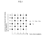
- Fig. 1 is a two-dimensional figure showing a location relationship between luminance data Y 1 , Y 2 and color difference data C BV , C RV .
- the luminance data Y 1 marked as white circles are arranged on each line. That is, in the first field, the luminance data Y 1 are arranged on lines 99, 101, 103 and so on. In the second field, the luminance data Y 1 are arranged on lines 100, 102, 104 and so on.
- the luminance data Y 2 marked as black circles are arranged on each line.
- the luminance data Y 2 are arranged on lines 100, 102, 104, ..., 522, 524 and so on.
- the luminance data Y 2 are arranged on lines 99, 101, 103, ... 523, 525 and so on.
- each of the color difference data C BV and C RV has the same sampling point as that of the luminance data Y 1 on the line of the white circle. That is, in the first field, the color difference data C BV and C RV are arranged on lines 99, 101, 103 and so on. In the second field, the color difference data C BV and C RV are arranged on lines 100, 102, 104 and so on. Therefore the sampling data of the color difference data C BV and C RV locate at the same position as that in the interlace system. In other words, the color difference data C BV and C RV are arranged on lines 99, 103, 107 and so on in the first field and the color difference data C BV and C RV are arranged on lines 101, 105, 109 and so on in the second field.
- Fig. 2 shows charts explaining the 4:2:0p serial data and converted 4:2:2 interlaced serial data, respectively.
- a line multiplexing the luminance data Y 1 and color difference data C BV , C RV is combined with a line multiplexing only luminance data Y 2 in pairs and the color difference data C BV , C RV , the luminance data Y 1 and Y 2 at the same horizontal picture element position as C BV , C RV and Y 1 are progressively multiplexed in the order on a transmission package equivalent to one interlaced line period.
- the color difference data C BV and the luminance data Y 1 at the horizontal picture element position 0 on the line 99 are combined with the luminance data Y 2 at the horizontal picture element position 0 on the line 100 in pairs.
- the color difference data C BV and C RV , luminance data Y 1 and luminance data Y 2 are progressively multiplexed in the order on the transmission package equivalent to one interlaced line period.
- the color difference data C BV , C RV and the luminance data Y 1 at the horizontal picture element position 1 on the line 99 are combined with the luminance data Y 2 at the horizontal picture element position 1 on the line 100 in pairs.
- the 4:2:0p serial data are generated as aforementioned.
- One of two adjacent lines of 4:2:0p data is set to a first line for multiplexing the luminance data Y 1 and the color difference data C BV , C RV .
- the other line is set to a second line for multiplexing the luminance data Y 2 only.
- the first line is combined with the second line in a pair.
- a pair of the luminance data Y 1 and the color difference data C BV , C RV on the first line and the luminance data Y 1 at the same horizontal picture element position as Y 1 C BV and C RV on the second line is demultiplexed from the 4:2:0p serial data.
- pairs of the luminance data Y 1 and the color difference data C BV at the horizontal picture element position 0 on the line 99 and the luminance data Y 2 at the horizontal picture element position 0 on the line 100 are demultiplexed from the 4:2:0p serial data.
- An arithmetic mean value of the luminance data Y 1 on the first line and the luminance data Y 2 on the second line is calculated.
- the arithmetic mean value of the luminance data Y 1 at the horizontal picture element position 0 on the line 99 and the luminance data Y 2 at the horizontal picture element position 0 on the line 100 is calculated.
- the calculated arithmetic mean value is set as the luminance data containing 4:2:2 signals.
- the above-obtained luminance data and the demultiplexed color difference data C BV on the second line are combined in pairs.
- the color difference data C BV and the calculated luminance data are multiplexed progressively in the order, generating 4:2:2 serial data at a horizontal picture element position 0.
- the arithmetic mean value of the luminance data Y 1 at the horizontal picture element position 0 on the line 99 and the luminance data Y 2 at the horizontal picture element position 0 on the line 100 is combined with the color difference data C BV at the horizontal picture element position 0 on the line 99 for multiplexing as shown in Fig. 2.
- the 4:2:2 serial data at the horizontal picture element position 0 are generated.
- the 4:2:2 serial data at the horizontal picture element position 1 are generated by using the luminance data Y 1 and the color difference data C RV at the horizontal picture element position 1 on the line 99 and the luminance data Y 2 at the horizontal picture element position 1 on the line 100.
- the luminance data for multiplexing are defined by the arithmetic mean value of the luminance data Y 1 and the luminance data Y 2 . Therefore the location of the luminance data resulting from this calculation is at a center between the first and the second lines imaginarily. Although the luminance data are shifted from the color difference data by a half of one line, the video quality is hardly influenced by such shifting.
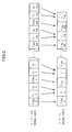
- Fig. B is a block diagram of the converter.
- a reference numeral 1 is a demultiplex circuit. Upon receiving an input of 4:2:0p serial data, the demultiplex circuit 1 extracts luminance data Y 1 , color difference data C BV , C RV on the first line and the luminance data Y 2 at the same horizontal picture element position as Y 1 , C BV , C RV on the second line.
- Reference numeral 2 and 3 are an adder and a multiplier, respectively.
- An arithmetic mean value of the luminance data Y 1 and Y 2 is calculated by the adder 2 and the multiplier 3. That is, the demultiplexed luminance data Y 1 and Y 2 are summed up and output by the adder 2.
- the output of the adder 2 is multiplied by 1/2 by the multiplier 3 that outputs the arithmetic mean value of the luminance data Y 1 and Y 2 .
- a reference numeral 4 is a data multiplex circuit which combines the output from the multiplier 3 (the arithmetic mean value of the luminance data Y 1 and Y 2 ) with the color difference data C BV , C RV at the same horizontal picture element position as the output in pairs and generates 4:2:2 interlace serial data by multiplexing the color difference data C BV , C RV and the luminance data (calculated arithmetic mean value) in the order.
- a reference numeral 5 is a clock recovery circuit which extracts a clock at 360 MHz from the input data.
- a reference numeral 6 is a PLL circuit which generates a clock at 270 MHz synchronized with the input data rate at 360 Mb/s.
- a pair of interlaced data is calculated by demultiplexing the 8:4:4 video data at every line in an interlacing manner and isolating the line complementing the demultiplexed line as another interlaced data.
- the respective data are extended twice on the time axis and transmitted as dual-link interface (Link A signal and Link B signal) having the same data structure as that of 525 interlace digital component signals at 13.5 MHz sampling for transmission.
- Fig. 4 shows a relationship between the link A signal and the link B signal in a vertical-time direction.
- the link A signal is formed of the luminance data and color difference data on lines 99, 101, 103 and so on in the first field and the luminance data and the color difference data on lines 100, 102, 104 and so on in the second field.
- the link B signal is formed of the luminance data and color difference data on lines 100, 102, 104 and so on in the first field and the luminance data and the color difference data on lines 99, 101, 103 and so on in the second field.
- the color difference data and the luminance data on each line are sequentially multiplexed in the order from the horizontal picture element position 0 to 719.
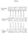
- Fig. 5 shows 4:2:2p transmission data and converted 4:2:2 interlace serial data, respectively.
- the color difference data CB and the luminance data Y at the horizontal picture element position 0 on the line 99 and then the color difference data CR and the luminance data Y at the horizontal picture element position 1 on the line 99 are arranged in the order progressively.
- the color difference data CB' and the luminance data Y' at the horizontal picture element position 0 on the line 100 and then the color difference data CR' and the luminance data Y' at the horizontal picture element 1 on the line 100 are arranged in the order progressively.
- the 4:2:2 interlace serial data are generated in the following manner.
- An arithmetic mean value of the color difference data CB of the link A signal at the horizontal picture element position 0 on the line 99 and the color difference data CB' of the link B signal at the horizontal picture element position 0 on the line 100 is calculated.
- the resultant arithmetic mean value is set as the color difference data CB" at the horizontal picture element position 0 on the line 50 in the 4:2:2 interlace.
- an arithmetic mean value of the luminance data Y of the link A signal at the horizontal picture element position 0 on the line 99 and the luminance data Y' of the link B signal at the horizontal picture element position 0 on the line 100 is calculated.
- the resultant arithmetic mean value is set as the luminance data Y" at the horizontal picture element position 0 on the line 50 in the 4:2:2 interlace.
- An arithmetic mean value of the color difference data CR of the link A signal at the horizontal picture element position 1 on the line 99 and the color difference data CR' of the link B signal at the horizontal picture element position 1 on the line 100 is calculated.
- the resultant arithmetic mean value is set as the color difference data CR" at the horizontal picture element position 1 on the line 50 in 4:2:2 interlace.
- an arithmetic mean value of the luminance data Y of the link A signal at the horizontal picture element position 1 on the line 99 and the luminance data Y' of the link B signal at the horizontal picture element position 1 on the line 100 is calculated.
- the resultant arithmetic mean value is set as the luminance data Y" at the horizontal picture element position 1 on the line 50 in 4:2:2 interlace.
- the above generated data are arranged in the order of the color difference data CB", luminance data Y", color difference data CR" and the luminance data Y" as shown in Fig. 5, generating the 4:2:2 interlace serial data.
- Fig. 6 is a block diagram of the converter.
- a reference numeral 21 is a reception circuit for receiving the link A signal.
- the reception circuit 21 receives the 4:2:2p link A signal and generates a clock at 270 MHz synchronized with the link A signal.
- a reference numeral 22 is a reception circuit for receiving the link B signal.
- the reception circuit 22 receives the 4:2:2p link B signal and generates a clock at 270 MHz synchronized with the link B signal.
- a reference numeral 23 is a serial-parallel converter for the link A signal.
- the serial-parallel converter 23 converts serial data of the link A signal received by the reception circuit 21 into 10-bit parallel data based on the clock at 270 MHz.
- a reference numeral 24 is a serial-parallel converter for the link B signal.
- the serial-parallel converter 24 converts serial data of the link B signal received by the reception circuit 22 into 10-bit parallel data based on the clock at 270 MHz.
- a reference numeral 25 is a buffer memory for the link A signal.
- the buffer memory 25 outputs accumulated 10-bit parallel data of the link A signal synchronized with a clock at 270 MHz.
- a reference numeral 26 is a buffer memory for the link B signal.
- the buffer memory 26 outputs accumulated 10-bit parallel data of the link B signal synchronized with a clock at 270 MHz.
- the buffer memories 25 and 26 output color difference data and luminance data at the same horizontal picture element position.
- Reference numerals 27 and 28 are an adder and a multiplier, respectively.
- An arithmetic mean value of the link A signal and the link B signal is obtained by the adder 27 and the multiplier 28. That is, the color difference data CB, CR of the link A signal are added to the color difference data CB', CR' of the link B signal at the same horizontal picture element position as CB and CR by the adder 27 for outputting.
- the luminance data Y of the link A signal are also added to the luminance data Y' of the link B signal at the same horizontal picture element position as Y by the adder 27 for outputting.
- the multiplier 28 multiplies each output of the adder 27 by 1/2, thus providing the arithmetic mean value of the link A signal and the link B signal.
- a reference numeral 29 is a parallel-serial converter for converting the parallel data from the multiplier 28 into serial data.
- a reference numeral 30 is an output driver for outputting 4:2:2 serial data.
Description
- The present invention relates to the conversion of progressive scan data into interlaced data. More specifically, this invention relates to the conversion of 4:2:0p or 4:2:2p serial data into 4:2:2 interlaced data described in SMPTE294M.
- It is a recent trend that the progressive scan system has been replacing the interlace system conforming to the requirement of high image quality. As a conventional progressive scan system, 8:4:4 system is well known for sampling a luminance signal of 525p analogue signals at 27 MHZ and for sampling a color difference signal at 13.5MHz.
- The digital interface of the aforementioned progressive scan system has two types, 4:2:2p system and 4:2:0p system.
- EP-A-0 692 915 describes conversion from the 4:4:2p system to the 4:2:0p system and vice versa.
- The 4:2:2p system contains a pair of interlaced data obtained by demultiplexing the aforementioned 8:4:4 data on each line into an interlacing manner. A line complementing the demultiplexed line is set as another interlaced data. Then they are extended twice on a time axis for two bit-serial interfaces having the same data structure as that of 525 interlace digital component signals sampled at 13.5 MHz, respectively.
- The 4:2:0p serial data is generated by filtering only a color difference signal of the aforementioned 8:4:4 data with a vertical low-pass filter and subsample the 8:4:4 data that has been filtered into interlacing manner.
- Therefore a luminance signal has progressive scan data at 27 MHz sampling. The color difference signal has interlaced data at 6.75 MHz sampling in 4:2:0p. This 4:2:0p system executes transmission at 360 Mb/s that is the same as the transmission rate executed in the 4:2:2 interlace at 18MHz sampling. Therefore the 4:2:0p system that can use the equipment or IC originally designed for the 18MHz sample 4:2:2 system has become the object of attention in the relevant field. However in TV station, all video signals have not been already shifted into the progressive scan system. The conventional interlace system has been used in the TV station as well. In case of simple monitoring, the interlace monitor is usually used in spite of the progressive scan system.
- In European countries employing PAL system or SECAM system, standardization of the digital interface of the progressive scan system has been developed. The standard of the system similar to the above-described 4:2:0p and 4:2:2p systems excepting the number of scanning lines is expected to be established.
- Accordingly the technology of converting the video data of progressive scan system into the video data of interlace system has been increasingly demanded.
- Such technology of converting 4:2:0p data of a frequent use into the interlaced data has been particularly demanded. Features of methods and apparatus for converting 4:2:0p or 4:2:2p serial data into 4:2:2 interlaced data to be described below by way of example in illustration of the invention are that any deterioration of the video quality and the cost are minimised, and that the construction is simple.
- A particular method to be described below by way of example in illustration of the invention for converting 4:2:0p data containing a first line multiplexing luminance data and color difference data and a second line multiplexing only luminance data in pairs into 4:2:2 interlaced data includes the steps of demultiplexing 4:2:0p data into luminance data and color difference data at a predetermined horizontal picture element position on a first line, demultiplexing 4:2:0p data into luminance data at the predetermined horizontal picture element position on a second line, obtaining an arithmetic mean value of the demultiplexed luminance data on a first line and the demultiplexed luminance data on a second line, and generating 4:2:2 interlaced data at the predetermined horizontal picture element position by multiplexing the obtained arithmetic mean value as luminance data and the demultiplexed color difference data in pairs.
- A particular unit to be described below by way of example in illustration of the invention for converting 4:2:0p data containing a first line multiplexing luminance data and color difference data and a second line multiplexing only luminance data in pairs into 4:2:2 interlaced data includes means for demultiplexing 4:2:0p data into luminance data and color difference data at a predetermined horizontal picture element position on a first line, means for demultiplexing 4:2:0p data into luminance data at the predetermined horizontal picture element position on a second line, means for calculating an arithmetic mean value of the demultiplexed luminance data on a first line and the demultiplexed luminance data on a second line, and means for generating 4:2:2 interlaced data at the predetermined horizontal picture element position by demultiplexing the obtained arithmetic mean value as luminance data and the demultiplexed color difference data in pairs.
- A particular method to be described below by way of example in illustration of the invention for converting 4:2:2p data containing a link A signal and a link B signal into 4:2:2 interlaced data includes the steps of demultiplexing a link A signal of 4:2:2p data into luminance data and color difference data at a predetermined horizontal picture element position; demultiplexing a link B signal of 4:2:2p data into luminance data and color difference data at the predetermined horizontal picture element position; obtaining luminance data of 4:2:2 interlaced data by calculating an arithmetic mean value of the demultiplexed luminance data of the link A signal and the demultiplexed luminance data of the link B signal, obtaining color difference data of 4:2:2 interlaced data by calculating an arithmetic mean value of the demultiplexed color difference data of the link A signal and the demultiplexed color difference data of the link B signal, and generating 4:2:2 interlaced data at the predetermined horizontal picture element position by multiplexing the obtained luminance data and the calculated color difference data in pairs.
- A particular unit to be described below by way of example in illustration of the invention for converting data of progressive scan system that converts 4:2:2p data containing a link A signal and a link B signal into 4:2:2 interlaced data includes means for demultiplexing a link A signal of 4:2:2p data into luminance data and color difference data at a predetermined horizontal picture element position, means for demultiplexing a link B signal of 4:2:2p data into luminance data and color difference data at the predetermined horizontal picture element position, means for obtaining luminance data as 4:2:2 interlaced data by calculating an arithmetic mean value of the demultiplexed luminance data of the link A signal and the demultiplexed luminance data of the link B signal, means for obtaining color difference data of 4:2:2 interlaced data by calculating an arithmetic mean value of the demultiplexed color difference data of the link A signal and the demultiplexed color difference data of the link B signal, and means for generating 4:2:2 interlaced data at the predetermined horizontal picture element position by multiplexing the calculated luminance data and the calculated color difference data in pairs.
- The arrangements to be described allow 4:2:0p data or 4:2:2p data to be converted into 4:2:2 interlaced data through simplified steps whilst minimising any adverse influence upon the video quality.
- The converter to be described below has a simple construction, resulting in cost reduction.
- The following description and drawings disclose by means of examples the invention which is characterised in the appended claims, whose terms determine the scope of the protection sought.
- In the drawings:-
- Fig. 1 is a two dimensional figure of a location relationship among luminance data Y1, Y2 and color difference data CBV, CRV;
- Fig. 2 shows charts each representing 4:2:0p serial data and converted 4:2:2 serial data, respectively;
- Fig. 3 is a block diagram of a converter that converts 4:2:0p serial data into the 4:2:2 serial data;
- Fig. 4 is a two-dimensional figure of a location relationship between a link A signal and a link B signal in view of vertical-time direction;
- Figs. 5 shows charts each representing 4:2:2p serial data and converted 4:2:2 serial data, respectively; and
- Fig. 6 is a block diagram of a conversion unit that converts 4:2:2p serial data into 4:2:2 serial data.
-
- Embodiments illustrative of the present invention will be described below in detail.
- The structure of 4:2:0p serial data (progressive scan data) is first described.
- The 4:2:0p data has line multiplexing luminance data Y1 and color difference data CBV and CRV combined with a line multiplexing only luminance data Y2 in pairs.
- The color difference data CBV and CRV are calculated by band limiting the color difference data CB and CR of the 8:4:4 data vertically to 1/2 of the luminance data and sub-sampling at every one line in an interlacing manner.
- Fig. 1 is a two-dimensional figure showing a location relationship between luminance data Y1, Y2 and color difference data CBV, CRV. The luminance data Y1 marked as white circles are arranged on each line. That is, in the first field, the luminance data Y1 are arranged on
lines lines - The luminance data Y2 marked as black circles are arranged on each line. In the first field, the luminance data Y2 are arranged on
lines lines - While each of the color difference data CBV and CRV has the same sampling point as that of the luminance data Y1 on the line of the white circle. That is, in the first field, the color difference data CBV and CRV are arranged on
lines lines lines lines 101, 105, 109 and so on in the second field. - Next the video data located in the above-described relationship is described. More specifically, the method of converting 4:2:0p serial data into the 4:2:2 serial data is described.
- Fig. 2 shows charts explaining the 4:2:0p serial data and converted 4:2:2 interlaced serial data, respectively.
- In the 4:2:0p serial data, a line multiplexing the luminance data Y1 and color difference data CBV, CRV is combined with a line multiplexing only luminance data Y2 in pairs and the color difference data CBV, CRV, the luminance data Y1 and Y2 at the same horizontal picture element position as CBV, CRV and Y1 are progressively multiplexed in the order on a transmission package equivalent to one interlaced line period.
- For example, the color difference data CBV and the luminance data Y1 at the horizontal
picture element position 0 on theline 99 are combined with the luminance data Y2 at the horizontalpicture element position 0 on theline 100 in pairs. Then the color difference data CBV and CRV, luminance data Y1 and luminance data Y2 are progressively multiplexed in the order on the transmission package equivalent to one interlaced line period. Subsequently the color difference data CBV, CRV and the luminance data Y1 at the horizontalpicture element position 1 on theline 99 are combined with the luminance data Y2 at the horizontalpicture element position 1 on theline 100 in pairs. - The 4:2:0p serial data are generated as aforementioned.
- The method for converting the above generated 4:2:0p serial data into the 4:2:2 serial data (interlace) is described.
- One of two adjacent lines of 4:2:0p data is set to a first line for multiplexing the luminance data Y1 and the color difference data CBV, CRV. The other line is set to a second line for multiplexing the luminance data Y2 only.
- The first line is combined with the second line in a pair. A pair of the luminance data Y1 and the color difference data CBV, CRV on the first line and the luminance data Y1 at the same horizontal picture element position as Y1 CBV and CRV on the second line is demultiplexed from the 4:2:0p serial data.
- For example, supposing that the
lines line 99 is set as the first line and theline 100 as the second line, pairs of the luminance data Y1 and the color difference data CBV at the horizontalpicture element position 0 on theline 99 and the luminance data Y2 at the horizontalpicture element position 0 on theline 100 are demultiplexed from the 4:2:0p serial data. - An arithmetic mean value of the luminance data Y1 on the first line and the luminance data Y2 on the second line is calculated. For example, the arithmetic mean value of the luminance data Y1 at the horizontal
picture element position 0 on theline 99 and the luminance data Y2 at the horizontalpicture element position 0 on theline 100 is calculated. - The calculated arithmetic mean value is set as the luminance data containing 4:2:2 signals. The above-obtained luminance data and the demultiplexed color difference data CBV on the second line are combined in pairs. The color difference data CBV and the calculated luminance data are multiplexed progressively in the order, generating 4:2:2 serial data at a horizontal
picture element position 0. For example, the arithmetic mean value of the luminance data Y1 at the horizontalpicture element position 0 on theline 99 and the luminance data Y2 at the horizontalpicture element position 0 on theline 100 is combined with the color difference data CBV at the horizontalpicture element position 0 on theline 99 for multiplexing as shown in Fig. 2. As a result, the 4:2:2 serial data at the horizontalpicture element position 0 are generated. - Similarly the 4:2:2 serial data at the horizontal
picture element position 1 are generated by using the luminance data Y1 and the color difference data CRV at the horizontalpicture element position 1 on theline 99 and the luminance data Y2 at the horizontalpicture element position 1 on theline 100. - The luminance data for multiplexing are defined by the arithmetic mean value of the luminance data Y1 and the luminance data Y2. Therefore the location of the luminance data resulting from this calculation is at a center between the first and the second lines imaginarily. Although the luminance data are shifted from the color difference data by a half of one line, the video quality is hardly influenced by such shifting.
- A converter illustrative of the present invention is now described in detail.
- Fig. B is a block diagram of the converter.
- In Fig. 3, a
reference numeral 1 is a demultiplex circuit. Upon receiving an input of 4:2:0p serial data, thedemultiplex circuit 1 extracts luminance data Y1, color difference data CBV, CRV on the first line and the luminance data Y2 at the same horizontal picture element position as Y1, CBV, CRV on the second line. -
Reference numeral adder 2 and themultiplier 3. That is, the demultiplexed luminance data Y1 and Y2 are summed up and output by theadder 2. The output of theadder 2 is multiplied by 1/2 by themultiplier 3 that outputs the arithmetic mean value of the luminance data Y1 and Y2. - A
reference numeral 4 is a data multiplex circuit which combines the output from the multiplier 3 (the arithmetic mean value of the luminance data Y1 and Y2) with the color difference data CBV, CRV at the same horizontal picture element position as the output in pairs and generates 4:2:2 interlace serial data by multiplexing the color difference data CBV, CRV and the luminance data (calculated arithmetic mean value) in the order. - A
reference numeral 5 is a clock recovery circuit which extracts a clock at 360 MHz from the input data. - A
reference numeral 6 is a PLL circuit which generates a clock at 270 MHz synchronized with the input data rate at 360 Mb/s. - A method for converting the 4:2:2p data into the 4:2:2 interlaced data is now described.
- The structure of the 4:2:2p serial data (progressive scan data) is described first.
- In the 4:2:2p system, a pair of interlaced data is calculated by demultiplexing the 8:4:4 video data at every line in an interlacing manner and isolating the line complementing the demultiplexed line as another interlaced data. The respective data are extended twice on the time axis and transmitted as dual-link interface (Link A signal and Link B signal) having the same data structure as that of 525 interlace digital component signals at 13.5 MHz sampling for transmission.
- Fig. 4 shows a relationship between the link A signal and the link B signal in a vertical-time direction.
- As Fig. 4 shows, the link A signal is formed of the luminance data and color difference data on
lines lines - The link B signal is formed of the luminance data and color difference data on
lines lines - The color difference data and the luminance data on each line are sequentially multiplexed in the order from the horizontal
picture element position 0 to 719. - The method for converting the 4:2:2p serial data into the 4:2:2 serial data is now described.
- Fig. 5 shows 4:2:2p transmission data and converted 4:2:2 interlace serial data, respectively.
- In the 4:2:2p link A signal, the color difference data CB and the luminance data Y at the horizontal
picture element position 0 on theline 99 and then the color difference data CR and the luminance data Y at the horizontalpicture element position 1 on theline 99 are arranged in the order progressively. - In the 4:2:2p link B signal, the color difference data CB' and the luminance data Y' at the horizontal
picture element position 0 on theline 100 and then the color difference data CR' and the luminance data Y' at thehorizontal picture element 1 on theline 100 are arranged in the order progressively. - Based on the aforementioned link A signal and link B signal, the 4:2:2 interlace serial data are generated in the following manner.
- An arithmetic mean value of the color difference data CB of the link A signal at the horizontal
picture element position 0 on theline 99 and the color difference data CB' of the link B signal at the horizontalpicture element position 0 on theline 100 is calculated. The resultant arithmetic mean value is set as the color difference data CB" at the horizontalpicture element position 0 on theline 50 in the 4:2:2 interlace. Then an arithmetic mean value of the luminance data Y of the link A signal at the horizontalpicture element position 0 on theline 99 and the luminance data Y' of the link B signal at the horizontalpicture element position 0 on theline 100 is calculated. The resultant arithmetic mean value is set as the luminance data Y" at the horizontalpicture element position 0 on theline 50 in the 4:2:2 interlace. An arithmetic mean value of the color difference data CR of the link A signal at the horizontalpicture element position 1 on theline 99 and the color difference data CR' of the link B signal at the horizontalpicture element position 1 on theline 100 is calculated. The resultant arithmetic mean value is set as the color difference data CR" at the horizontalpicture element position 1 on theline 50 in 4:2:2 interlace. Then an arithmetic mean value of the luminance data Y of the link A signal at the horizontalpicture element position 1 on theline 99 and the luminance data Y' of the link B signal at the horizontalpicture element position 1 on theline 100 is calculated. The resultant arithmetic mean value is set as the luminance data Y" at the horizontalpicture element position 1 on theline 50 in 4:2:2 interlace. - The above generated data are arranged in the order of the color difference data CB", luminance data Y", color difference data CR" and the luminance data Y" as shown in Fig. 5, generating the 4:2:2 interlace serial data.
- A converter illustrative of the present invention is now described in detail.
- Fig. 6 is a block diagram of the converter.
- In Fig. 6, a
reference numeral 21 is a reception circuit for receiving the link A signal. Thereception circuit 21 receives the 4:2:2p link A signal and generates a clock at 270 MHz synchronized with the link A signal. Areference numeral 22 is a reception circuit for receiving the link B signal. Thereception circuit 22 receives the 4:2:2p link B signal and generates a clock at 270 MHz synchronized with the link B signal. - A
reference numeral 23 is a serial-parallel converter for the link A signal. The serial-parallel converter 23 converts serial data of the link A signal received by thereception circuit 21 into 10-bit parallel data based on the clock at 270 MHz. - A
reference numeral 24 is a serial-parallel converter for the link B signal. The serial-parallel converter 24 converts serial data of the link B signal received by thereception circuit 22 into 10-bit parallel data based on the clock at 270 MHz. - A
reference numeral 25 is a buffer memory for the link A signal. Thebuffer memory 25 outputs accumulated 10-bit parallel data of the link A signal synchronized with a clock at 270 MHz. - A
reference numeral 26 is a buffer memory for the link B signal. Thebuffer memory 26 outputs accumulated 10-bit parallel data of the link B signal synchronized with a clock at 270 MHz. - That is the
buffer memories -
Reference numerals adder 27 and themultiplier 28. That is, the color difference data CB, CR of the link A signal are added to the color difference data CB', CR' of the link B signal at the same horizontal picture element position as CB and CR by theadder 27 for outputting. The luminance data Y of the link A signal are also added to the luminance data Y' of the link B signal at the same horizontal picture element position as Y by theadder 27 for outputting. Themultiplier 28 multiplies each output of theadder 27 by 1/2, thus providing the arithmetic mean value of the link A signal and the link B signal. - A
reference numeral 29 is a parallel-serial converter for converting the parallel data from themultiplier 28 into serial data. - A
reference numeral 30 is an output driver for outputting 4:2:2 serial data.
Claims (5)
- A method for converting 4:2:0p data containing a first line multiplexing luminance data and color difference data and a second line multiplexing only luminance data in pairs into 4:2:2 interlaced data including the steps of:demultiplexing 4:2:0p data into luminance data and color difference data at a predetermined horizontal picture element position on a first line;demultiplexing 4:2:0p data into luminance data at said predetermined horizontal picture element position on a second line;obtaining an arithmetic mean value of said demultiplexed luminance data on a first line and said demultiplexed luminance data on a second line; andgenerating 4:2:2 interlaced data at said predetermined horizontal picture element position by multiplexing said obtained arithmetic mean value as luminance data and said demultiplexed color difference data in pairs.
- A method for converting 4:2:2p data containing a link A signal and a link B signal into 4:2:2 interlaced data including the steps of:demultiplexing a link A signal of 4:2:2p data into luminanced data and color difference data at a predetermined horizontal picture element position;demultiplexing a link B signal of 4:2:2p data into luminance data and color difference data at said predetermined horizontal picture element position;obtaining luminance data of 4:2:2 interlaced data by calculating an arithmetic mean value of said demultiplexed luminance data of said link A signal and said demultiplexed luminance data of said link B signal;obtaining color difference data of 4:2:2 interlaced data by calculating an arithmetic mean value of said demultiplexed color difference data of said link A signal and said demultiplexed color difference data of said link B signal; andgenerating 4:2:2 interlaced data at said predetermined horizontal picture element position by multiplexing said obtained luminance data and said calculated color difference data in pairs.
- A unit for converting 4:2:0p data containing a first line multiplexing luminance data and color difference data and a second line multiplexing only luminance data in pairs into 4:2:2 interlaced data including:means (1) for demultiplexing 4:2:0p data into luminance data and color difference data at a predetermined horizontal picture element position on a first line;means (4) for demultiplexing 4:2:0p data into luminance data at said predetermined horizontal picture element position on a second line;means (2, 3) for calculating an arithmetic mean value of said demultiplexed luminance data on a first line and said demultiplexed luminance data on a second line; andmeans (4) for generating 4:2:2 interlaced data at said predetermined horizontal picture element position by multiplexing said obtained arithmetic mean value as luminance data and said demultiplexed color difference data in pairs.
- A unit for converting 4:2:0p data containing a first line multiplexing luminance data and color difference data combined with a second line multiplexing only luminance data in pairs into 4:2:2 interlaced data comprising:means (5) for generating a first clock synchronized with 4:2:0p data;means (6) for generating a second clock synchronized with 4:2:2 interlaced data based on said first clock;means (1) for demultiplexing 4:2:0p data into luminance data and color difference data at a predetermined horizontal picture element position on a first line and luminance data at said predetermined horizontal picture element position on a second line based on said first clock;an adder (2) for adding said demultiplexed luminance data on a first line to said demultiplexed luminance data on a second line;a multiplier (3) for multiplying an output of said adder by 1/2; andmultiplex means (4) for generating 4:2:2 interlaced data at said predetermined horizontal picture element position by multiplexing a pair of luminance data output from said multiplier and said demultiplexed color difference data based on said second clock.
- A unit for converting data of progressive scan system that converts 4:2:2p data containing a link A signal and a link B signal into 4:2:2 interlaced data including:means (21, 23, 25) for demultiplexing a link A signal of 4:2:2p data into luminance data and color difference data at a predetermined horizontal picture element position;means (22, 24, 26) for demultiplexing a link B signal of 4:2:2p data into luminance data and color difference data at said predetermined horizontal picture element position;means (27, 28) for obtaining luminance data as 4:2:2 interlaced data by calculating an arithmetic mean value of said demultiplexed luminance data of said link A signal and said demultiplexed luminance data of said link B signal;means (27, 28) for obtaining color difference data of 4:2:2 interlaced data by calculating an arithmetic mean value of said demultiplexed color difference data of said link A signal and said demultiplexed color difference data of said link B signal; andmeans (30) for generating 4:2:2 interlaced data at said predetermined horizontal picture element position by multiplexing said calculated luminance data and said calculated color difference data in pairs.
Applications Claiming Priority (3)
| Application Number | Priority Date | Filing Date | Title |
|---|---|---|---|
| JP801196 | 1996-01-22 | ||
| JP8008011A JP2936315B2 (en) | 1996-01-22 | 1996-01-22 | Conversion method of transmission data of progressive scanning method and its conversion device |
| JP8011/96 | 1996-01-22 |
Publications (3)
| Publication Number | Publication Date |
|---|---|
| EP0785677A2 EP0785677A2 (en) | 1997-07-23 |
| EP0785677A3 EP0785677A3 (en) | 1998-07-01 |
| EP0785677B1 true EP0785677B1 (en) | 2002-01-02 |
Family
ID=11681418
Family Applications (1)
| Application Number | Title | Priority Date | Filing Date |
|---|---|---|---|
| EP97300371A Expired - Lifetime EP0785677B1 (en) | 1996-01-22 | 1997-01-21 | Method and apparatus for converting progressive scan data into interlaced data |
Country Status (5)
| Country | Link |
|---|---|
| US (1) | US5835152A (en) |
| EP (1) | EP0785677B1 (en) |
| JP (1) | JP2936315B2 (en) |
| CA (1) | CA2195612A1 (en) |
| DE (1) | DE69709415T2 (en) |
Families Citing this family (7)
| Publication number | Priority date | Publication date | Assignee | Title |
|---|---|---|---|---|
| US6529244B1 (en) | 1999-12-22 | 2003-03-04 | International Business Machines Corporation | Digital video decode system with OSD processor for converting graphics data in 4:4:4 format to 4:2:2 format by mathematically combining chrominance values |
| TWI249359B (en) * | 2004-12-22 | 2006-02-11 | Realtek Semiconductor Corp | Method and apparatus for simultaneous progressive and interlaced display |
| JP5232319B2 (en) | 2011-10-20 | 2013-07-10 | 株式会社東芝 | Communication apparatus and communication method |
| JP5694412B2 (en) * | 2011-10-20 | 2015-04-01 | 株式会社東芝 | Transmission device, reception device, transmission method, and reception method |
| JP5390667B2 (en) | 2012-06-11 | 2014-01-15 | 株式会社東芝 | Video transmission device and video reception device |
| JP5689938B2 (en) * | 2013-10-07 | 2015-03-25 | 株式会社東芝 | Video transmission equipment |
| JP5808509B2 (en) * | 2015-01-22 | 2015-11-10 | 株式会社東芝 | Video receiver |
Family Cites Families (6)
| Publication number | Priority date | Publication date | Assignee | Title |
|---|---|---|---|---|
| US4335393A (en) * | 1980-04-15 | 1982-06-15 | Harris Video Systems, Inc. | Method and system using sequentially encoded color and luminance processing of video type signals to improve picture quality |
| DE3930964A1 (en) * | 1989-09-15 | 1991-03-28 | Thomson Brandt Gmbh | TELEVISION TRANSMISSION SYSTEM |
| GB2238688B (en) * | 1989-11-27 | 1994-01-12 | Sony Corp | Methods of and apparatus for digital video signal processing |
| JP2936299B2 (en) * | 1993-07-22 | 1999-08-23 | 日本テレビ放送網株式会社 | Signal transmission / recording and input / output method |
| DE69522504T2 (en) * | 1994-06-14 | 2002-05-08 | Matsushita Electric Ind Co Ltd | Video signal recording device and video signal recording and display device |
| JP2933487B2 (en) * | 1994-07-15 | 1999-08-16 | 松下電器産業株式会社 | How to convert chroma format |
-
1996
- 1996-01-22 JP JP8008011A patent/JP2936315B2/en not_active Expired - Fee Related
-
1997
- 1997-01-21 CA CA002195612A patent/CA2195612A1/en not_active Abandoned
- 1997-01-21 DE DE69709415T patent/DE69709415T2/en not_active Expired - Fee Related
- 1997-01-21 EP EP97300371A patent/EP0785677B1/en not_active Expired - Lifetime
- 1997-01-22 US US08/785,948 patent/US5835152A/en not_active Expired - Fee Related
Also Published As
| Publication number | Publication date |
|---|---|
| US5835152A (en) | 1998-11-10 |
| CA2195612A1 (en) | 1997-07-23 |
| EP0785677A2 (en) | 1997-07-23 |
| JPH09200801A (en) | 1997-07-31 |
| DE69709415T2 (en) | 2002-09-05 |
| DE69709415D1 (en) | 2002-02-07 |
| JP2936315B2 (en) | 1999-08-23 |
| EP0785677A3 (en) | 1998-07-01 |
Similar Documents
| Publication | Publication Date | Title |
|---|---|---|
| EP0076547B1 (en) | Television system for high-definition television and a television transmitter and receiver suitable therefor | |
| US5136380A (en) | Display signal device and method for providing compatibility between ntsc television and hdtv | |
| US6266093B1 (en) | Color video camera method and system | |
| US4967272A (en) | Bandwidth reduction and multiplexing of multiple component TV signals | |
| WO1990013980A1 (en) | Scan converter for a high definition television system | |
| KR970008461B1 (en) | Television signal generating apparatus and video signal processing apparatus | |
| EP0785677B1 (en) | Method and apparatus for converting progressive scan data into interlaced data | |
| CA1258524A (en) | Method and system for improved reconstruction of video images in line sequential chroma format | |
| KR0154134B1 (en) | Muse/ntsc scanning line conversion system | |
| US5128750A (en) | Television signal converter for converting a high definition television signal into a television signal for display by a standard television receiver | |
| US5227879A (en) | Apparatus for transmitting an extended definition TV signal having compatibility with a conventional TV system | |
| CA2203735A1 (en) | Up-converter and scanning line conversion method | |
| CA2000709A1 (en) | Compatible extended-definition television | |
| EP0804029A2 (en) | Video signal processing apparatus | |
| JP3097403B2 (en) | Video signal transmitting device and video signal receiving device | |
| JPH04504790A (en) | TV transmission system with additional signals | |
| JPH04185085A (en) | Television signal transfer system | |
| Bathe | HDMAC encoder—first generation: Experience and applications | |
| JP2001275131A (en) | Video signal transmission method and transmitter and receiver to perform it | |
| JPS63114389A (en) | Encoder for edtv system | |
| JPH0231558B2 (en) | JUNJISOSAHENKANSOCHI | |
| JPH0472980A (en) | Method and apparatus for video signal constitution | |
| JPH04192692A (en) | Television signal transmission system | |
| JPH06335027A (en) | Method for generating television signal | |
| JPH04286497A (en) | Color difference signal demodulation circuit |
Legal Events
| Date | Code | Title | Description |
|---|---|---|---|
| PUAI | Public reference made under article 153(3) epc to a published international application that has entered the european phase |
Free format text: ORIGINAL CODE: 0009012 |
|
| AK | Designated contracting states |
Kind code of ref document: A2 Designated state(s): DE GB IT NL |
|
| PUAL | Search report despatched |
Free format text: ORIGINAL CODE: 0009013 |
|
| AK | Designated contracting states |
Kind code of ref document: A3 Designated state(s): DE GB IT NL |
|
| 17P | Request for examination filed |
Effective date: 19980609 |
|
| GRAG | Despatch of communication of intention to grant |
Free format text: ORIGINAL CODE: EPIDOS AGRA |
|
| 17Q | First examination report despatched |
Effective date: 20010315 |
|
| GRAG | Despatch of communication of intention to grant |
Free format text: ORIGINAL CODE: EPIDOS AGRA |
|
| GRAH | Despatch of communication of intention to grant a patent |
Free format text: ORIGINAL CODE: EPIDOS IGRA |
|
| GRAH | Despatch of communication of intention to grant a patent |
Free format text: ORIGINAL CODE: EPIDOS IGRA |
|
| GRAA | (expected) grant |
Free format text: ORIGINAL CODE: 0009210 |
|
| REG | Reference to a national code |
Ref country code: GB Ref legal event code: IF02 |
|
| AK | Designated contracting states |
Kind code of ref document: B1 Designated state(s): DE GB IT NL |
|
| PGFP | Annual fee paid to national office [announced via postgrant information from national office to epo] |
Ref country code: GB Payment date: 20020115 Year of fee payment: 6 |
|
| PGFP | Annual fee paid to national office [announced via postgrant information from national office to epo] |
Ref country code: NL Payment date: 20020131 Year of fee payment: 6 |
|
| REF | Corresponds to: |
Ref document number: 69709415 Country of ref document: DE Date of ref document: 20020207 |
|
| PGFP | Annual fee paid to national office [announced via postgrant information from national office to epo] |
Ref country code: DE Payment date: 20020326 Year of fee payment: 6 |
|
| PLBE | No opposition filed within time limit |
Free format text: ORIGINAL CODE: 0009261 |
|
| STAA | Information on the status of an ep patent application or granted ep patent |
Free format text: STATUS: NO OPPOSITION FILED WITHIN TIME LIMIT |
|
| 26N | No opposition filed | ||
| PG25 | Lapsed in a contracting state [announced via postgrant information from national office to epo] |
Ref country code: GB Free format text: LAPSE BECAUSE OF NON-PAYMENT OF DUE FEES Effective date: 20030121 |
|
| PG25 | Lapsed in a contracting state [announced via postgrant information from national office to epo] |
Ref country code: NL Free format text: LAPSE BECAUSE OF NON-PAYMENT OF DUE FEES Effective date: 20030801 Ref country code: DE Free format text: LAPSE BECAUSE OF NON-PAYMENT OF DUE FEES Effective date: 20030801 |
|
| GBPC | Gb: european patent ceased through non-payment of renewal fee | ||
| NLV4 | Nl: lapsed or anulled due to non-payment of the annual fee |
Effective date: 20030801 |
|
| PG25 | Lapsed in a contracting state [announced via postgrant information from national office to epo] |
Ref country code: IT Free format text: LAPSE BECAUSE OF NON-PAYMENT OF DUE FEES Effective date: 20050121 |