EP0783109A1 - Kraftmessvorrichtung mit kapazitivem Geber - Google Patents
Kraftmessvorrichtung mit kapazitivem Geber Download PDFInfo
- Publication number
- EP0783109A1 EP0783109A1 EP96402871A EP96402871A EP0783109A1 EP 0783109 A1 EP0783109 A1 EP 0783109A1 EP 96402871 A EP96402871 A EP 96402871A EP 96402871 A EP96402871 A EP 96402871A EP 0783109 A1 EP0783109 A1 EP 0783109A1
- Authority
- EP
- European Patent Office
- Prior art keywords
- state
- during
- control signal
- charge
- capacitor
- Prior art date
- Legal status (The legal status is an assumption and is not a legal conclusion. Google has not performed a legal analysis and makes no representation as to the accuracy of the status listed.)
- Granted
Links
Images


Classifications
-
- G—PHYSICS
- G01—MEASURING; TESTING
- G01P—MEASURING LINEAR OR ANGULAR SPEED, ACCELERATION, DECELERATION, OR SHOCK; INDICATING PRESENCE, ABSENCE, OR DIRECTION, OF MOVEMENT
- G01P15/00—Measuring acceleration; Measuring deceleration; Measuring shock, i.e. sudden change of acceleration
- G01P15/02—Measuring acceleration; Measuring deceleration; Measuring shock, i.e. sudden change of acceleration by making use of inertia forces using solid seismic masses
- G01P15/08—Measuring acceleration; Measuring deceleration; Measuring shock, i.e. sudden change of acceleration by making use of inertia forces using solid seismic masses with conversion into electric or magnetic values
- G01P15/125—Measuring acceleration; Measuring deceleration; Measuring shock, i.e. sudden change of acceleration by making use of inertia forces using solid seismic masses with conversion into electric or magnetic values by capacitive pick-up
Definitions
- the present invention relates to a measurement device with a capacitive sensor such as for example a device for measuring a force and in particular an inertial force corresponding to an acceleration of the device.
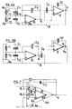
- FIG. 1 of the accompanying drawings shows a diagram of this known measuring device. It essentially comprises a capacitive sensor 1 in which a conductive strip 2 suspended elastically forms an armature common to two capacitors C 1 and C 2 . This blade is intended to move under the influence of a force whose intensity is to be known, this displacement varying the capacities of the two capacitors.
- the capacitive sensor thus arranged is connected to an interface circuit 3 whose output 4 produces a voltage which is a function of the capacities of the two capacitors C 1 and C 2 and which therefore represents the position of the movable blade and consequently l sought intensity of force.
- the interface circuit 3 permanently adjusts the potential of the mobile blade 2, called potential V m , so that any flow of charges in this blade is canceled for the measurement. There is therefore a load balancing, qualifier which is commonly given to this kind of measuring device (whose English name is "load balancing device").
- the interface circuit 3 comprises an integration block 5 with a capacitor C f cooperating with an operational amplifier 6.
- This integration block permanently supplies at its output 4 the potential V m equal to the integral of the charges supplied to its input by the circuit blocks which are connected to it upstream.
- phase 1 The operation of the interface circuit 3 is cyclical in the sense that it is divided into two phases which are continuously repeated. These phases are designated by "phase 1" and “phase 2" in the following description.
- the sequence of these phases is controlled by clock signals which may have a first state Ph 1 and a second state Ph 2 . They are generated by a phase control generator Cph which applies them to switches preferably of the transistorized type. These are closed as appropriate during one of phases 1 or 2 and open during the opposite phase. In the figures of the appended drawings, these switches are designated by circles containing a 1 or a 2 depending on whether they are closed during phase 1 or phase 2 respectively under the action of the signals Ph 1 and Ph 2 .
- the interface circuit 3 further comprises a switching block 7 comprising switches 7-1 to 7-4 arranged so that during phase 1, the fixed armatures of the two capacitors C 1 and C 2 are brought respectively to supply potentials V 0 and -V 0 , while during phase 2, these armatures and the fixed plate of the capacitors C 1 and C 2 are at the same potential V m brought back from the output 4 on switches 7-3 and 7-4 by a connection 8.
- the supply potentials V 0 and -V 0 are symmetrical with respect to a supply potential dc which serves as a reference for the output potential V m .
- the interface circuit further comprises a charge transfer block 9 comprising a capacitor C 3 called “measurement” and an operational amplifier 10 forming together an integrator, two transfer capacitors C 30 and C 4 , as well as switches 11 - 1 to 11-4, switch 11-1 being closed during phase 1 and the other three during phase 2.
- a charge transfer block 9 comprising a capacitor C 3 called “measurement” and an operational amplifier 10 forming together an integrator, two transfer capacitors C 30 and C 4 , as well as switches 11 - 1 to 11-4, switch 11-1 being closed during phase 1 and the other three during phase 2.
- This interface circuit finally comprises a compensation block 12 intended to ensure a reduction, or even the cancellation of the influence of the stray capacitances which are present in the sensor 1.
- This compensation block comprises a compensation capacitor C c and switches 13-1 and 13-2 closed respectively during phases 1 and 2.
- V m VS 1 - VS 2 + Cp 1 - Cp 2 VS 1 + VS 2 + Cp 1 + Cp 2 - VS 3 VS 4 CC .
- V 0 in which the potentials V m and V 0 are respectively those indicated in FIG. 1 and the capacities C 1 and C 2 those of the capacitors there having identical designations, while Cp 1 and Cp 2 are the values of the parasitic capacities of the sensor 1 .
- capacitors C 1 and C 2 are respectively in parallel with two parasitic resistances r 1 and r 2 .
- These resistors can conduct currents i 1 and i 2 during the measurement phase so that the currents from capacitors C 1 and C 2 due to their respective charges and sent to the integrator formed by the capacitor C 3 and the amplifier 10, are increased by a parasitic current I p .
- This total current is formed by the difference of the currents i 1 and i 2 flowing respectively through the resistors r 1 and r 2 .
- FIGS. 3A and 3B partially represent the blocks 7 and 9, as well as the capacitive sensor 1 of FIG. 1, respectively in phase 1 of precharging or measurement and in phase 2 of resetting or discharging of the capacitors.
- the switches 7-3 and 7-4 short-circuit not only the capacitors of the sensor 1, but also the parasitic resistances r 1 and r 2 .
- V i V m - 1 VS 3 ⁇ ( VS 1 - VS 2 ) V 0 - ( VS 1 + VS 2 ) V m ⁇
- FIGS. 4A and 4B partially show the block 9 connected to the block 5 respectively during phases 1 and 2.
- the capacitor C4 is at the potential V i
- this capacitor is at the potential V m , transmitted without modification by the amplifier 10.
- V m The value of V m thus becomes equal to:
- a first way to reduce this error would be to reduce the integration time T as much as possible, or in other words, to increase the sampling frequency punctuating the successive executions of phases 1 and 2.
- the invention aims to provide a solution to the problem of reducing the influence of parasitic resistances of a load balancing sensor without going through the disadvantageous methods set out above.
- FIG. 5 represents a preferred embodiment of the measuring device according to the invention.
- the diagram of this device is identical to that of FIG. 1 as regards the switching block 7, the sensor 1, the compensation block 12 and the integration block 5.
- it differs from it according to the invention by the arrangement of the charge transfer block designated here by the reference 9A instead of 9.
- This charge transfer block 9A comprises the following elements already described: the measurement capacitor C 3 , the transfer capacitor C 4 , the operational amplifier 10 and the generator Cph generating the signals Ph 1 and Ph 2 . However, these components are connected differently than in the prior art measuring device.
- the capacitor C 3 is connected in parallel to a switch 14 which, unlike the diagram in FIG. 1, is closed during phase 1 instead of being closed during phase 2.
- the non-inverting input 10a of the operational amplifier 10 is connected directly to the connection 8 and therefore receives the signal from the output 4 (potential V m ) whatever the phase in which the measuring device is located.
- the capacitor C 4 is associated with a set of four switches 15-1 to 15-4 connected in the following manner.
- the switch 15-1 closed during phase 2, connects the output 10b of the amplifier 10 to one of the plates 16 of the capacitor C4.
- the other armature 17 of this capacitor C 4 is connected to the capacitor C c by means of the switch 15-2 closed during phase 1.
- the armature 16 of the capacitor C4 is also connected to the switch 15-3 closed during phase 1 and which connects it during this phase to the non-inverting input 6a of the amplifier 6.
- the armature 17 is also connected to the switch 15-4 closed during phase 2 and which connects it to the connection 8 during this phase.
- FIGS. 6A and 6B show the measuring device according to the invention respectively during phases 1 and 2 which, for the convenience of the description, are said to be “measuring” and “charge transfer” respectively.
- the switches and the compensation block 12 are not shown.
- FIG. 6A also shows that during the measurement phase, the charge of the capacitor C 4 is reset to zero, since it is then connected to the input terminals of the amplifier 6 which are at the same potential.
- V i V m + 1 VS 3 ⁇ ( VS 1 - VS 2 ) V 0 - ( VS 1 + VS 2 ) V m ⁇ in which the sign "-" of equation (2) is replaced by the sign "+”, while, thanks to the invention, one can dispense with deducing from the value of the potential V i , a value ⁇ V i due to parasitic resistances. These therefore no longer have any influence on the result of the measurement.
- FIG. 7 proposes an advantageous embodiment of such a compensation circuit.
- the inverting input 10c of the operational amplifier 10 is connected to a compensation capacitor C 5 which is mounted in parallel to a switch 18-1 closed during phase 2. This capacitor is also connected to a switch 18-2 closed during phase 1 and also connected to the non-inverting input of amplifier 10.
- the whole forms an operational amplifier 10A with offset compensation in which during phase 1, the offset is measured, while during phase 2, the value of this offset is subtracted from the potential at the inverting input 10b of the amplifier 10.
Applications Claiming Priority (2)
| Application Number | Priority Date | Filing Date | Title |
|---|---|---|---|
| FR9515476 | 1995-12-26 | ||
| FR9515476A FR2742868B1 (fr) | 1995-12-26 | 1995-12-26 | Dispositif de mesure d'une force a l'aide d'un capteur capacitif |
Publications (2)
| Publication Number | Publication Date |
|---|---|
| EP0783109A1 true EP0783109A1 (de) | 1997-07-09 |
| EP0783109B1 EP0783109B1 (de) | 2001-05-30 |
Family
ID=9485943
Family Applications (1)
| Application Number | Title | Priority Date | Filing Date |
|---|---|---|---|
| EP96402871A Expired - Lifetime EP0783109B1 (de) | 1995-12-26 | 1996-12-23 | Kraftmessvorrichtung mit kapazitivem Geber |
Country Status (4)
| Country | Link |
|---|---|
| US (1) | US5821421A (de) |
| EP (1) | EP0783109B1 (de) |
| DE (1) | DE69613092T2 (de) |
| FR (1) | FR2742868B1 (de) |
Cited By (1)
| Publication number | Priority date | Publication date | Assignee | Title |
|---|---|---|---|---|
| US6377056B1 (en) | 1998-08-26 | 2002-04-23 | Hitachi, Ltd. | Electrostatic capacitance type dynamical quantity sensor |
Families Citing this family (4)
| Publication number | Priority date | Publication date | Assignee | Title |
|---|---|---|---|---|
| JP4178658B2 (ja) * | 1998-06-30 | 2008-11-12 | 株式会社デンソー | 容量式物理量検出装置 |
| US7614300B2 (en) * | 2007-05-30 | 2009-11-10 | Northrop Grumman Corporation | System and method for mitigating errors in electrostatic force balanced instrument |
| US7652486B2 (en) * | 2008-01-17 | 2010-01-26 | Freescale Semiconductor, Inc. | Capacitance detection circuit including voltage compensation function |
| US10712360B2 (en) | 2017-09-27 | 2020-07-14 | Azoteq (Pty) Ltd | Differential charge transfer based accelerometer |
Citations (2)
| Publication number | Priority date | Publication date | Assignee | Title |
|---|---|---|---|---|
| FR2706038A1 (fr) * | 1993-06-02 | 1994-12-09 | Suisse Electronique Microtech | Dispositif de mesure d'une force. |
| FR2720510A1 (fr) * | 1994-05-26 | 1995-12-01 | Suisse Electronique Microtech | Dispositif de mesure d'une force. |
Family Cites Families (3)
| Publication number | Priority date | Publication date | Assignee | Title |
|---|---|---|---|---|
| US3877313A (en) * | 1973-07-23 | 1975-04-15 | Singer Co | Electrostatic accelerometer |
| US4584885A (en) * | 1984-01-20 | 1986-04-29 | Harry E. Aine | Capacitive detector for transducers |
| FR2689627B1 (fr) * | 1992-04-07 | 1997-06-20 | Sextant Avionique | Perfectionnement aux micro-capteurs pendulaires asservis. |
-
1995
- 1995-12-26 FR FR9515476A patent/FR2742868B1/fr not_active Expired - Fee Related
-
1996
- 1996-12-23 DE DE69613092T patent/DE69613092T2/de not_active Expired - Lifetime
- 1996-12-23 EP EP96402871A patent/EP0783109B1/de not_active Expired - Lifetime
- 1996-12-26 US US08/780,168 patent/US5821421A/en not_active Expired - Lifetime
Patent Citations (2)
| Publication number | Priority date | Publication date | Assignee | Title |
|---|---|---|---|---|
| FR2706038A1 (fr) * | 1993-06-02 | 1994-12-09 | Suisse Electronique Microtech | Dispositif de mesure d'une force. |
| FR2720510A1 (fr) * | 1994-05-26 | 1995-12-01 | Suisse Electronique Microtech | Dispositif de mesure d'une force. |
Non-Patent Citations (1)
| Title |
|---|
| H.LEUTHOLD ET AL.: "An ASIC for High-resolution Capacitive Microaccelerometers", SENSORS AND ACTUATORS, vol. A21-A23, 1990, LAUSANNE CH, pages 278 - 281, XP002013866 * |
Cited By (2)
| Publication number | Priority date | Publication date | Assignee | Title |
|---|---|---|---|---|
| US6377056B1 (en) | 1998-08-26 | 2002-04-23 | Hitachi, Ltd. | Electrostatic capacitance type dynamical quantity sensor |
| DE19940422C2 (de) * | 1998-08-26 | 2003-04-24 | Hitachi Ltd | Sensor mit kapazitivem Element zur Erfassung einer dynamischen Größe |
Also Published As
| Publication number | Publication date |
|---|---|
| DE69613092T2 (de) | 2002-01-24 |
| EP0783109B1 (de) | 2001-05-30 |
| DE69613092D1 (de) | 2001-07-05 |
| FR2742868B1 (fr) | 1998-02-13 |
| FR2742868A1 (fr) | 1997-06-27 |
| US5821421A (en) | 1998-10-13 |
Similar Documents
| Publication | Publication Date | Title |
|---|---|---|
| EP1962063B1 (de) | Automatischer Test einer elektronischen Schaltungsanordnung eines kapazitiven Sensors, und elektronische Schaltungsanordnung zur Ausführung des Testes | |
| EP0377388B1 (de) | Wellenformgenerator eines analogen Signals | |
| EP1835263B1 (de) | Elektronischer Schnittstellenschaltkreis eines kapazitiven Sensors zur Messung eines physikalischen Parameters und Verfahren zur Ingangsetzung des elektronischen Schaltkreises | |
| FR2916855B1 (fr) | Systeme d'instrument a balance de forces, instrument a balance de forces et procede pour attenuer une erreur dans un tel instrument | |
| FR2509048A1 (fr) | Dispositif transducteur de pression capacitif a caracteristique lineaire | |
| EP2131494B1 (de) | Schaltkreis mit geschalteten Kapazitäten mit geringem Energieverbrauch | |
| EP0783109B1 (de) | Kraftmessvorrichtung mit kapazitivem Geber | |
| FR2491243A1 (fr) | Dispositif pour le traitement d'un signal electrique variable par multiplexage | |
| FR2582461A1 (fr) | Filtre a decimation | |
| WO1991011812A2 (fr) | Circuit d'echantillonnage de signaux analogiques | |
| EP0042641B1 (de) | Frequenzdemodulator mit einer Verzögerungsschaltung, wobei die Verzögerung von der empfangenen Frequenz abhängig ist | |
| EP0017301B1 (de) | Modulator zur Frequenzverschiebung | |
| FR2720510A1 (fr) | Dispositif de mesure d'une force. | |
| FR2706038A1 (fr) | Dispositif de mesure d'une force. | |
| EP0076737A1 (de) | Symmetrischer Integrator und dessen Anwendung in einem Filter | |
| EP0226490B1 (de) | Synchrones Filter mit geschalteten Kapazitäten | |
| EP0143024B1 (de) | Mit geschalteten Kapazitäten durchgeführter exponentieller Integrator mit erhöhter Zeitkonstante | |
| FR2699307A1 (fr) | Procédé et dispositif pour la convolution analogique d'images. | |
| EP0130873B1 (de) | Bandpassfilter mit geschalteten Kapazitäten | |
| FR2604835A1 (fr) | Amplificateur a capacites commutees a gain eleve | |
| CH689496A5 (fr) | Dispositif de mesure d'une force muni d'un capteur capacitif. | |
| EP0615344A1 (de) | Verbesserter Kodierer zur Rauschformung, insbesondere Sigma/Delta-Kodierer | |
| EP0130107B1 (de) | Filter mit geschalteten Kapazitäten zur Simulation eines LC-Filters | |
| EP0010039A1 (de) | Filtervorrichtung mit einer Ladungsverschiebeanordnung | |
| FR2829599A1 (fr) | Circuit de commande de bus |
Legal Events
| Date | Code | Title | Description |
|---|---|---|---|
| PUAI | Public reference made under article 153(3) epc to a published international application that has entered the european phase |
Free format text: ORIGINAL CODE: 0009012 |
|
| AK | Designated contracting states |
Kind code of ref document: A1 Designated state(s): CH DE ES FR GB IT LI NL |
|
| 17P | Request for examination filed |
Effective date: 19971210 |
|
| GRAG | Despatch of communication of intention to grant |
Free format text: ORIGINAL CODE: EPIDOS AGRA |
|
| 17Q | First examination report despatched |
Effective date: 20000825 |
|
| GRAG | Despatch of communication of intention to grant |
Free format text: ORIGINAL CODE: EPIDOS AGRA |
|
| GRAH | Despatch of communication of intention to grant a patent |
Free format text: ORIGINAL CODE: EPIDOS IGRA |
|
| GRAH | Despatch of communication of intention to grant a patent |
Free format text: ORIGINAL CODE: EPIDOS IGRA |
|
| GRAA | (expected) grant |
Free format text: ORIGINAL CODE: 0009210 |
|
| AK | Designated contracting states |
Kind code of ref document: B1 Designated state(s): CH DE ES FR GB IT LI NL |
|
| PG25 | Lapsed in a contracting state [announced via postgrant information from national office to epo] |
Ref country code: NL Free format text: LAPSE BECAUSE OF FAILURE TO SUBMIT A TRANSLATION OF THE DESCRIPTION OR TO PAY THE FEE WITHIN THE PRESCRIBED TIME-LIMIT Effective date: 20010530 |
|
| REG | Reference to a national code |
Ref country code: CH Ref legal event code: EP |
|
| REF | Corresponds to: |
Ref document number: 69613092 Country of ref document: DE Date of ref document: 20010705 |
|
| ITF | It: translation for a ep patent filed |
Owner name: BIANCHETTI - BRACCO - MINOJA S.R.L. |
|
| GBT | Gb: translation of ep patent filed (gb section 77(6)(a)/1977) |
Effective date: 20010810 |
|
| NLV1 | Nl: lapsed or annulled due to failure to fulfill the requirements of art. 29p and 29m of the patents act | ||
| PG25 | Lapsed in a contracting state [announced via postgrant information from national office to epo] |
Ref country code: ES Free format text: LAPSE BECAUSE OF FAILURE TO SUBMIT A TRANSLATION OF THE DESCRIPTION OR TO PAY THE FEE WITHIN THE PRESCRIBED TIME-LIMIT Effective date: 20011130 |
|
| REG | Reference to a national code |
Ref country code: CH Ref legal event code: PUE Owner name: C.S.E.M. CENTRE SUISSE D'ELECTRONIQUE ET DE MICROT Ref country code: CH Ref legal event code: NV Representative=s name: CSEM CENTRE SUISSE D'ELECTRONIQUE ET DE MICROTECHN |
|
| REG | Reference to a national code |
Ref country code: GB Ref legal event code: IF02 |
|
| RAP2 | Party data changed (patent owner data changed or rights of a patent transferred) |
Owner name: COLIBRYS S.A. |
|
| REG | Reference to a national code |
Ref country code: GB Ref legal event code: 732E |
|
| REG | Reference to a national code |
Ref country code: FR Ref legal event code: TP |
|
| PLBE | No opposition filed within time limit |
Free format text: ORIGINAL CODE: 0009261 |
|
| STAA | Information on the status of an ep patent application or granted ep patent |
Free format text: STATUS: NO OPPOSITION FILED WITHIN TIME LIMIT |
|
| 26N | No opposition filed | ||
| REG | Reference to a national code |
Ref country code: CH Ref legal event code: NV Representative=s name: CHRISTOPHE SAAM PATENTS & TECHNOLOGY SURVEYS SA |
|
| REG | Reference to a national code |
Ref country code: CH Ref legal event code: PCAR Free format text: PATENTS & TECHNOLOGY SURVEYS SA;RUE DES TERREAUX 7 CASE POSTALE 2848;2001 NEUCHATEL (CH) |
|
| REG | Reference to a national code |
Ref country code: CH Ref legal event code: PFA Owner name: COLIBRYS SA Free format text: COLIBRYS SA#MALADIERE 83#2007 NEUCHATEL (CH) -TRANSFER TO- COLIBRYS SA#MALADIERE 83#2007 NEUCHATEL (CH) |
|
| REG | Reference to a national code |
Ref country code: FR Ref legal event code: PLFP Year of fee payment: 20 |
|
| PGFP | Annual fee paid to national office [announced via postgrant information from national office to epo] |
Ref country code: DE Payment date: 20151211 Year of fee payment: 20 Ref country code: GB Payment date: 20151221 Year of fee payment: 20 Ref country code: CH Payment date: 20151221 Year of fee payment: 20 |
|
| PGFP | Annual fee paid to national office [announced via postgrant information from national office to epo] |
Ref country code: FR Payment date: 20151221 Year of fee payment: 20 |
|
| PGFP | Annual fee paid to national office [announced via postgrant information from national office to epo] |
Ref country code: IT Payment date: 20151228 Year of fee payment: 20 |
|
| REG | Reference to a national code |
Ref country code: DE Ref legal event code: R071 Ref document number: 69613092 Country of ref document: DE |
|
| REG | Reference to a national code |
Ref country code: CH Ref legal event code: PL |
|
| REG | Reference to a national code |
Ref country code: GB Ref legal event code: PE20 Expiry date: 20161222 |
|
| PG25 | Lapsed in a contracting state [announced via postgrant information from national office to epo] |
Ref country code: GB Free format text: LAPSE BECAUSE OF EXPIRATION OF PROTECTION Effective date: 20161222 |