EP0780962A2 - Electronically commuted motor - Google Patents
Electronically commuted motor Download PDFInfo
- Publication number
- EP0780962A2 EP0780962A2 EP96119750A EP96119750A EP0780962A2 EP 0780962 A2 EP0780962 A2 EP 0780962A2 EP 96119750 A EP96119750 A EP 96119750A EP 96119750 A EP96119750 A EP 96119750A EP 0780962 A2 EP0780962 A2 EP 0780962A2
- Authority
- EP
- European Patent Office
- Prior art keywords
- motor
- microprocessor
- reset
- input
- hall
- Prior art date
- Legal status (The legal status is an assumption and is not a legal conclusion. Google has not performed a legal analysis and makes no representation as to the accuracy of the status listed.)
- Granted
Links
Images


Classifications
-
- H—ELECTRICITY
- H02—GENERATION; CONVERSION OR DISTRIBUTION OF ELECTRIC POWER
- H02P—CONTROL OR REGULATION OF ELECTRIC MOTORS, ELECTRIC GENERATORS OR DYNAMO-ELECTRIC CONVERTERS; CONTROLLING TRANSFORMERS, REACTORS OR CHOKE COILS
- H02P23/00—Arrangements or methods for the control of AC motors characterised by a control method other than vector control
- H02P23/0077—Characterised by the use of a particular software algorithm
-
- H—ELECTRICITY
- H02—GENERATION; CONVERSION OR DISTRIBUTION OF ELECTRIC POWER
- H02P—CONTROL OR REGULATION OF ELECTRIC MOTORS, ELECTRIC GENERATORS OR DYNAMO-ELECTRIC CONVERTERS; CONTROLLING TRANSFORMERS, REACTORS OR CHOKE COILS
- H02P6/00—Arrangements for controlling synchronous motors or other dynamo-electric motors using electronic commutation dependent on the rotor position; Electronic commutators therefor
- H02P6/34—Modelling or simulation for control purposes
-
- H—ELECTRICITY
- H02—GENERATION; CONVERSION OR DISTRIBUTION OF ELECTRIC POWER
- H02H—EMERGENCY PROTECTIVE CIRCUIT ARRANGEMENTS
- H02H7/00—Emergency protective circuit arrangements specially adapted for specific types of electric machines or apparatus or for sectionalised protection of cable or line systems, and effecting automatic switching in the event of an undesired change from normal working conditions
- H02H7/08—Emergency protective circuit arrangements specially adapted for specific types of electric machines or apparatus or for sectionalised protection of cable or line systems, and effecting automatic switching in the event of an undesired change from normal working conditions for dynamo-electric motors
- H02H7/093—Emergency protective circuit arrangements specially adapted for specific types of electric machines or apparatus or for sectionalised protection of cable or line systems, and effecting automatic switching in the event of an undesired change from normal working conditions for dynamo-electric motors against increase beyond, or decrease below, a predetermined level of rotational speed
Definitions
- the invention relates to an electronically commutated motor with control of functions by a microprocessor or microcontroller, hereinafter called the microprocessor.
- German patent application P 44 42 450.7 is concerned with this problem.
- This uses motor-controlled reset processes which are distinguished from the reset process which occurs when the device is switched on by an additional signal at an input of the microprocessor, which is provided there by a memory cell. This allows the motor to run safely.
- the microprocessor becomes defective, the motor stator windings will continue to receive current and become overheated.
- a free input of the microprocessor to which such an external memory cell can be connected is not always available, since in some cases all inputs of the microprocessor are required for the desired additional functions of the motor.
- this object is achieved by an electronically commutated motor with control of functions by a microprocessor or microcontroller, hereinafter referred to as the microprocessor, and with a watchdog timer arranged outside the microprocessor, which receives its reset pulses from a rotor position sensor of the motor, or another by the rotation of the motor directly actuated sensor, in order to prevent triggering of this timing element at least above a predetermined motor speed during operation of the motor.
- Watchdog timers are known in the context of microprocessors and it is common to provide reset pulses from the microprocessor as long as it is functioning properly. However, this does not provide security against malfunctions of the microprocessor, because it may very well be that the microprocessor continues to emit reset pulses, but that there is a defect at one of its outputs, which then leads to overheating of the motor controlled by this output.
- the motor is advantageously designed such that the watchdog timer contains a multivibrator with a low oscillation frequency, which is kept in the deactivated state when the motor is running, by signals generated when the motor rotates, at least above a predetermined motor speed.
- the watchdog timer therefore only comes into action when the engine speed falls below the specified value or when the engine has come to a standstill.
- a particularly advantageous embodiment of the invention is distinguished characterized in that the multivibrator periodically discharges a capacitor in the activated state, which belongs to a power-up reset circuit of the microprocessor and is connected to a reset input of this microprocessor, and in that the multivibrator is periodically activated when it is activated and without the microprocessor being switched on , interrupts the stator current of the motor, especially with a low duty cycle.
- the fact that the watchdog timer interrupts the stator current of the motor when it responds, i.e. not via the microprocessor, provides a high level of security against failure of the microprocessor, since the remaining parts of the motor circuit continue to function in this case and ensure that the engine does not overheat.
- the low duty cycle creates long pauses in which no current flows in the motor, so that there is no risk of the motor overheating.
- ECM electronically commutated motor
- the invention is suitable for any type of motor, and this motor can also be a collector motor, provided that it generates control impulses during its rotation, for example by a tachometer generator or a Hall generator arranged in or on the motor.
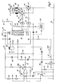
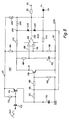
- the permanent magnetic rotor of the motor 20 is indicated schematically at 22 and the two strands of its stator winding have the reference numerals 24 and 26. As shown, these are connected to a positive line 28, which e.g. + 12 V, + 24 V or + 48 V compared to the potential of a negative lead 30.
- An npn Darlington transistor 32 is used to control the current i 1 in the strand 24, and a corresponding transistor 34 for controlling the current i 2 in the strand 26, both of which are provided with a free-wheeling diode 32 'and 34'.
- the emitters of both transistors 32, 34 are connected to the negative line 30, their collectors to the strands 24 and 26, respectively.
- the base of the transistor 32 is controlled by an AND gate 38 via a resistor 40, as is the base of the transistor 34 by an AND gate 42 via a resistor 44.
- An input of the AND gate 38, which in FIG. 1 is P1 is connected to the output C1 of a microprocessor 50, the other via a resistor 48 with a positive supply line 52 of, for example, + 5 V, as well corresponding input of the AND gate 42, and the anode of a diode 54, the cathode of which is connected to the output 58 of an operational amplifier 56.
- the other input of the AND gate 42 is connected to the output C2 of the microprocessor 50.
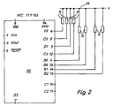
- the individual connections of the microprocessor 50 here a 4-bit microprocessor of type 17P103 (manufacturer NEC), are shown schematically in FIG. As can be seen, the connections B0, B1, B2, C0, C3, D0, D1, D2 are each connected via a resistor R to the positive line 52 (+5 V). This resistance R can e.g. have a value of 47 k ⁇ .
- a Hall IC 60 is arranged in the vicinity of the rotor 22, which is shown again on the lower left in FIG. 1 and which generates rectangular "Hall" pulses during operation, which are shown schematically in FIG. 1. These are fed via a resistor 62 to the input D3 of the microprocessor 50, further via a first differentiating element (resistor 64 and capacitor 66) to the reset input RESET / of the microprocessor 50, and via a second differentiating element (capacitor 68, resistor 70) of the base 71 NPN transistor 72, the emitter of which is connected to the negative line 30 and the collector of which is connected to the negative input 74 of the operational amplifier 56.
- a capacitor 76 is arranged between this input 74 and the negative line 30, and a resistor 78 between this input 74 and the output 58.
- a resistor 80 is arranged between the plus input 82 of the operational amplifier 56 and its output 58, and this plus input 82 is located at the connection point 84 of two resistors 86, 88, of which the former is connected to the plus line 52 and the latter to the minus line 30.
- a resistor 90 lies between the output 58 and the positive line 52.
- a resistor 92 connects this output to a node 94, which is connected to the negative line 30 via a capacitor 96 and to the reset input 3 of the microprocessor 50 via a resistor 98 is.
- the input 3 is also connected to the anode of a diode 100, the cathode of which is connected to the positive line 52. This prevents the reset input RESET / from adopting a higher potential than the positive line 52.
- a ceramic resonator 102 (8 MHz) is connected to the inputs XIN and XOUT of the microprocessor 50 as the clock generator. Between the input V 00 of the microprocessor 50 and its input GND there is a capacitor 104 which prevents interference pulses from reaching the microprocessor 50 via the positive line 52.
- the Hall signal is fed to the input D3 of the microprocessor 50 via the resistor 62, so that the microprocessor can properly control the commutation signals at the outputs C1 and C2, as will be explained below of the flowchart of FIG. 7 is described and explained in detail.
- the resistor 62 prevents the Hall signal from being short-circuited in the event of an internal short circuit or a fault in the microprocessor 50 and therefore represents an important safety feature, because without this resistor 62 the cyclical reset process would no longer be possible in this case.
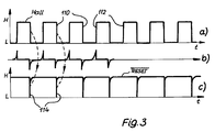
- the Hall signal (FIG. 3a) is differentiated via the capacitor 66 and supplied in a differentiated form (FIG. 3b) to the RESET / microprocessor 50 input.
- this input On every negative edge 110 of the Hall signal, this input is briefly pulled to 0 V, that is to the potential of the negative line 30, and on every positive edge 112 this RESET input receives a more positive potential for a short time, but as soon as it is 5.7 V exceeds, is derived via the diode 100 and buffered by the capacitor 104 so that the microprocessor 50 is not damaged or destroyed by this signal.
- the Hall IC 60 Since the Hall IC 60 has an open collector output, it has a pull-up resistor 64 which makes the output 61 of the Hall IC 60 positive when its internal output transistor is turned off.
- the capacitor 68 and the resistor 70 form a differentiator, which generates a positive pulse on each positive edge 112 of the Hall signal, which briefly renders the transistor 72 conductive, causing it to briefly pull the minus input 74 of the operational amplifier 56 to 0 V and thereby the capacitor 76 discharges.
- the operational amplifier 56 forms, together with its passive components, a so-called watchdog timer 120, which is referred to below as a WD timer.
- a watchdog timer 120 This term is used to denote a circuit which is intended to prevent a microprocessor 50 from "hanging up” due to interference pulses or the like, that is to say it stops somewhere in its program and refuses to work.
- the WD timer 120 only does not take action if it is continuously supplied with so-called refresh pulses which prevent it from becoming active, and in the present case it receives these refresh pulses via the differentiator 68, 70 and the transistor 72.
- Fig. 4 shows the procedure just described.
- the Hall signals are shown as the speed decreases. Their positive edges 112 cause the positive pulses u 71 shown in FIG. 4b at the base 71 of the transistor 72, and these pulses cause the capacitor 76 to be continuously discharged as long as the motor 20 is running, ie the motor 20 as long as it is running the refresh signals for the WD timer 120, so that it cannot be activated while the engine 20 is running.
- This change in potential is delayed by the resistor 92 and the capacitor 96 and fed to the microprocessor 50 as a watchdog reset signal via the resistor 98.
- the microprocessor 50 in this case carries out a power-up reset, just as when switching on: when switching on, the capacitor 96 is discharged, ie the RESET / input initially has the potential 0 V, and Only when the capacitor 96 has charged via the resistors 90 and 92 does this input receive the signal high. This automatically creates a power-up reset process when the motor 20 is switched on.
- the diode 54 becomes conductive, so that the corresponding inputs of the AND gates 38 and 42 receive a correspondingly low potential and both transistors 32 and 34 are blocked as long as the output 58 is low.
- the capacitor 76 is discharged via the resistor 78, and therefore after some time the potential at the minus input 74 again becomes more negative than the potential at the plus input 82, as a result of which the output 58 becomes high again. As a result, that of the transistors 32, 34 which receives a corresponding commutation signal from the microprocessor 50 becomes conductive again and the motor 20 tries to start again.
- the pulses Hall arise again, which periodically discharge the capacitor 76 and deactivate the WD timer 120.
- the cycle described is repeated, i.e. the WD timer 120 oscillates at a very low frequency, e.g. 0.2 Hz, continuously gives reset pulses to the microprocessor 50, and switches the transistor 32 or 34, e.g. one second and four seconds off, so that the motor 20 cannot overheat, but will start again if the blockage is no longer present. This is called an anti-lock device with automatic restart.
- the motor 20 is completely switched off by the process described, which is advantageous because during the reset process, possibly undefined states at the outputs C1 and C2 of the Microprocessor 50 could occur. However, since the motor 20 cannot receive any current during this reset process, this does not interfere, which is a further advantage of the invention.
- a PWM signal from a PWM actuator 122 at point P1 that is to say the anode of diode 54, and the pulse duty factor of this PWM actuator 122 would then be set to 0% if the potential at output 58 became 0 V will.
- This variant is indicated in Fig. 1 with dashed lines; in this case the diode 54 would be omitted.
- the PWM controller 122 can be part of a current controller or a speed controller (not shown).
- full-bridge circuit (not shown) is used to control the motor 20, its switching elements must be latched to one another in a known manner, so that a short circuit in this full-bridge circuit is reliably avoided even if a fault occurs in the microprocessor 50.
- Corresponding circuits for full bridge circuits are known.
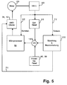
- FIG. 5 shows the basic structure of the circuit according to FIG. 1 in the form of a block diagram.
- the Hall IC 60 is coupled to the motor 20 and, when the motor 20 rotates, it supplies refresh pulses to the WD timer 120 via the transistor 72, so that the latter is kept in the non-activated state.
- Hall IC 60 also provides cyclic reset signals to microprocessor 50 (via capacitor 66) and a power-up reset occurs via capacitor 96 and resistor 98 at startup.
- the AND gates 38, 42 are controlled via the signal at point P1, which is supplied by the WD timer 120.
- the microprocessor 50 itself is periodically reset when the motor 20 is running by means of a cyclical reset process 66, or - when switched on - via the power-up reset 96, 98, or - when the motor 20 is blocked - via the WD timer 120. These alternative possibilities are symbolized by an OR symbol 130.
- the microprocessor 50 receives the Hall commutation signals from the Hall IC 60 so that it controls the motor 20 correctly.
- step S130 the program, controlled by the address counter of the microprocessor 50, jumps to step S130, where a brief initialization can be carried out if necessary.
- step S132 a query is made as to whether the memory cell RES_Bit1 in the microprocessor 50 is set. If this is the case, the program goes to step S134, where the same query for the internal memory cell RES_Bit2 takes place. If the answer is also positive here, the program goes to step S136, where it is queried whether the memory cells for the byte RES_Byte contain the value wxyz.
- step S138 a query is made as to whether the Hall signal is high. 3, since a cyclic reset process takes place only on the negative edge 110 of a Hall signal, the Hall signal must be low after a cyclic reset process, ie a high Hall signal means that there is no cyclical reset process may have taken place and it must be a power-up reset. Step S138 may also be omitted if steps S132, 134, 136 already provide a sufficiently high level of security.
- step S140 a cyclic reset process is carried out in step S140, and in this case no detailed initialization (step S142) is carried out, but only the program counter is reset to a specific value and started again, and the flowchart in this case continues to step S144, that is to say to the main program with commutation (if it is not a collector motor) and possibly speed control; Step S144 is explained below with reference to FIG. 7.
- Steps S132, 134, 136, and possibly 138, Fig. 6 are a key system, i.e. the program can only proceed to step S140 if it has the correct keys for the internal memory cells RES_Bit 1, 2 and the RES_Byte, and this is only the case if certain values have been loaded into these memory cells beforehand. This is not the case immediately after switching on, but then these memory cells have random values, so that immediately after switching on, the answer will always be NO in at least one of steps S132 to S136. With such a negative answer, the program goes to step S145, i.e. in this case, the program automatically recognizes that it must be a power-up reset.
- step S145 the internal memory cells RES_Bit1 and 2 are set, and the information wxyz is loaded into the RES_Byte, so that with each subsequent reset operation, the queries S132 to S136 are answered with YES and consequently only a cyclic reset operation is carried out.
- Step S145 is followed by step S142, where a detailed initialization is carried out after switching on, for example loading a rotational speed setpoint, querying registers, etc. Then the program also goes to step S144, that is to say the main program, which is in the form here a loop S146 is set up, for the passage of which a constant time is required, for example 80 ⁇ s, and which is run continuously during operation, but is interrupted by the cyclic reset processes (S140) on the negative edges 110 of the Hall signal.
- step S144 that is to say the main program, which is in the form here a loop S146 is set up, for the passage of which a constant time is required, for example 80 ⁇ s, and which is run continuously during operation, but is interrupted by the cyclic reset processes (S140) on the negative edges 110 of the Hall signal.
- Fig. 7 shows the structure of the main program.
- the main program is entered, following step S140 or S142 of FIG. 6.
- step S158 e.g. a speed control can take place, or other engine-specific functions.
- the program then goes back to step S152 via loop S146, and this loop S146 is continuously run through during operation, interrupted only by the cyclical reset processes (S140) on the negative edges 110 of the Hall signal, by interrupt processes, or by disturbances which occur Trigger WD timer 120.
- S140 cyclical reset processes
- the capacitor 76 of the WD timer 120 is discharged and does not start to charge until the motor 20 starts up. As soon as the motor 20 is running, the capacitor 76 is discharged again and again via the transistor 72 in the manner described. As a result, the motor 20 can be started normally without the WD timer 120 being activated.
- FIG. 8 shows a variant for the WD timer 120 of FIG. 1.
- This WD timer 170 is activated even at low speeds, the stronger the lower the speed becomes, the stronger. It is not activated at normal engine speeds.
- the Hall signals are supplied to the base of a pnp transistor 174 via a differentiator consisting of a capacitor 172 and a resistor 173, i.e. on the negative edges 110 of the Hall signal (cf. FIG. 3a), the transistor 174 becomes briefly conductive and supplies a charging pulse to a capacitor 176 (e.g. 10 nF) which is connected between its collector and the negative line 30.
- a capacitor 176 e.g. 10 nF
- npn transistor 178 The base of an npn transistor 178 is connected to the collector of transistor 174, the emitter of which is connected to positive line 52, via two resistors 180, 182, the connection point of which is designated 184. Furthermore, there is a resistor 186 between the base of the transistor 178 and the negative line 30. The emitter of the transistor 178 is connected to the negative line 30, its collector via a resistor 188 (for example 10 k) to the negative input 189 of a comparator 190.
- a capacitor 192 (eg 3.3 .mu.F) lies between the minus input 189 and the minus line 30. It has the same function as the capacitor 76 in FIG. 1.
- the plus input 194 of the comparator 190 is connected to the positive line 52 via a resistor 196 (e.g. 100 k) and to the minus line 30 via a resistor 198 (e.g. 100 k).
- a resistor 202 (eg 47 k) leads to the plus input 194, a resistor 204 (eg 2 k) to the plus line 52, and a resistor 206 (eg 470 k) to a node 208.
- a diode 210 lies between output 200 and node 208 (anode at output 200).
- a resistor 212 (e.g., 100 k) lies between node 208 and the collector of transistor 178.
- the WD timer 170 replaces the transistor 72 and the WD timer 120 in FIG. 1.
- the corresponding connecting elements are therefore indicated in FIG. 8, that is to say the resistor 92 and the diode 54.
- transistor 174 is briefly switched on by each differentiated negative edge 110 of Hall signal, as a result of which capacitor 176 is charged.
- a switch-on pulse of defined length is generated at transistor 178, which switches point B to the potential of negative line 30.
- the capacitor 192 discharges through the resistor 188.
- capacitor 192 is charged through resistor 204, diode 210, and resistors 212 and 188.
- the Hall signal has a high frequency, so that the capacitor 192 is only slightly charged since it is discharged again and again via the transistor 178 and the resistor 188. Consequently, the minus input 189 of the comparator 190 has a more negative potential than the plus input 194, and the comparator 190 has a high impedance at its output 200, so that it does not initiate a reset process and the diode 54 remains blocked, ie the motor 20 runs normally.
- the potential at the positive input 194 should expediently be set so high (by selecting the resistors 196, 198) that the voltage at the capacitor 192 can cover a large voltage range.
- the point B is less often connected by the transistor 178 to the negative line 30, and the charging of the capacitor 192 via the resistor 204, the diode 210 and the resistors 212 and 188 now prevails, so that the The minus input 189 of the comparator 190 becomes more positive than the plus input 194. This switches the output 200 to 0 V, there is a WD reset, and the output stage transistors 32 and 34 (FIG. 1) are blocked via the diode 54.
- the capacitor 192 discharges through the resistors 188, 212 and 206, and additionally by the pulses that continue to come from the Hall IC 60 (Fig. 1) of the motor still running, so that the OFF time, during which the comparator 190 has the potential 0 V at its output, which depends on the speed still present. The lower this becomes, the longer this OFF time, i.e. it is a dynamic overload protection for the motor 20.
- the OFF time is constant, since it is then only determined by the resistors 188, 212 and 206, via which the capacitor 192 discharges.
- the WD timer 170 according to FIG. 8 has particular advantages when starting up an engine. It may be that the motor is inhibited during start-up, but starts, but increases its speed only slowly. In this case, the timer 170 gives it more time to reach its operating speed because the capacitor 192 is partially discharged again and again as long as the motor is rotating.
- the timer 170 switches off the motor at some point so that it is not overloaded.
- the timer 170 switches the motor on again after a predetermined pause, and it is usually easier to start up the second time because the motor has already rotated. In addition, the timer 170 automatically shortens its OFF time when the engine is running.
- the switch-on time of the timer 170 is short and the switch-off time is long, which protects the motor against overheating but nevertheless ensures a restart if the motor has not been blocked.
- FIG. 9 shows a variant 170 '.
- the output 200 of the comparator 190 is connected to the point 184 via a diode 220, its anode being connected to this point. If the output 200 assumes the potential 0 V, the point 184 is also set to approximately 0 V, so that the transistor 178 can no longer be turned on. In this case, the OFF time is not dependent on the engine speed, but constant.
- timers 170, 170 'shown in FIGS. 8 and 9 can also be used in motors which are not controlled by a microprocessor, but by conventional commutation circuits.
Abstract
Description
Die Erfindung betrifft einen elektronisch kommutierten Motor mit Steuerung von Funktionen durch einen Mikroprozessor oder Mikrocontroller, im folgenden Mikroprozessor genannt.The invention relates to an electronically commutated motor with control of functions by a microprocessor or microcontroller, hereinafter called the microprocessor.
Bei derartigen Motoren tritt das Problem auf, daß durch elektrische Störsignale auf den Zuleitungen des Motors der Mikroprozessor gestört werden kann und sich dann ggf. "aufhängt", so daß der Motor zum Stillstand kommt. Dies kann. auftreten durch Bursts transienter Impulsgruppen, oder durch ESD-Signale (ESD = electrostatic discharge), also Signale durch elektrostatische Entladungen, wie sie in Umgebungen mit starken elektrischen Störungen auftreten können.In such motors, the problem arises that the microprocessor can be disturbed by electrical interference signals on the leads of the motor and then "hang up", so that the motor comes to a standstill. This can. occur through bursts of transient pulse groups, or through ESD signals (ESD = electrostatic discharge), i.e. signals due to electrostatic discharges, as can occur in environments with strong electrical interference.
Man versucht, sich hierbei dadurch zu helfen, daß man die Eingänge eines solchen Mikroprozessors mit entsprechenden Schutzschaltungen versieht, doch ist das aufwendig und führt nicht immer zum gewünschten Resultat.One tries to help oneself by providing the inputs of such a microprocessor with appropriate protective circuits, but this is complex and does not always lead to the desired result.
Mit diesem Problem beschäftigt sich die deutsche Patentanmeldung P 44 42 450.7 der Anmelderin. Diese verwendet motorgesteuerte Resetvorgänge, die von dem beim Einschalten auftretenden Resetvorgang durch ein zusätzliches Signal an einem Eingang des Mikroprozessors unterschieden werden, das dort durch eine Speicherzelle bereitgestellt wird. Damit läßt sich ein sicherer Lauf des Motors erreichen. Jedoch besteht die Gefahr, daß dann, wenn der Mikroprozessor defekt wird, die Statorwicklungen des Motors ständig Strom erhalten und überhitzt werden. Auch ist nicht in jedem Fall ein freier Eingang des Mikroprozessors verfügbar, an den eine solche externe Speicherzelle angeschlossen werden kann, da in manchen Fällen alle Eingänge des Mikroprozessors für gewünschte Zusatzfunktionen des Motors benötigt werden.The applicant's German
Es ist deshalb eine Aufgabe der Erfindung, einen neuen elektronisch kommutierten Motor bereitzustellen.It is therefore an object of the invention to provide a new electronically commutated motor.
Nach der Erfindung wird diese Aufgabe gelöst durch einen elektronisch kommutierten Motor mit Steuerung von Funktionen durch einen Mikroprozessor oder Mikrocontroller, im folgenden Mikroprozessor genannt, und mit einem außerhalb des Mikroprozessors angeordneten Watchdog-Zeitglied, welches seine Rückstellimpulse von einem Rotorstellungssensor des Motors, oder einem sonstigen durch die Drehung des Motors direkt betätigten Sensor, erhält, um im Betrieb des Motors eine Auslösung dieses Zeitglieds mindestens oberhalb einer vorgegebenen Motordrehzahl zu verhindern. - Watchdog-Zeitglieder sind im Zusammenhang mit Mikroprozessoren bekannt, und es ist üblich, diesen vom Mikroprozessor, solange dieser ordnungsgemäß funktioniert, Rückstellimpulse zuzuführen. Eine Sicherheit gegen Fehlfunktionen des Mikroprozessors ist damit aber nicht verbunden, denn es kann sehr wohl sein, daß der Mikroprozessor weiterhin Rückstellimpulse abgibt, daß aber an einem seiner Ausgänge ein Defekt vorliegt, der dann zu einer Überhitzung des von diesem Ausgang gesteuerten Motors führt.According to the invention, this object is achieved by an electronically commutated motor with control of functions by a microprocessor or microcontroller, hereinafter referred to as the microprocessor, and with a watchdog timer arranged outside the microprocessor, which receives its reset pulses from a rotor position sensor of the motor, or another by the rotation of the motor directly actuated sensor, in order to prevent triggering of this timing element at least above a predetermined motor speed during operation of the motor. Watchdog timers are known in the context of microprocessors and it is common to provide reset pulses from the microprocessor as long as it is functioning properly. However, this does not provide security against malfunctions of the microprocessor, because it may very well be that the microprocessor continues to emit reset pulses, but that there is a defect at one of its outputs, which then leads to overheating of the motor controlled by this output.
Dadurch, daß diese Rückstellimpulse nicht wie üblich vom Mikroprozessor, sondern vom Motor kommen und durch dessen Drehung ausgelöst werden, wird die Sicherheit der gesamten Anordnung wesentlich erhöht, denn wenn, aus welchen Gründen auch immer, der Motor nicht mehr läuft, bleiben die Rückstellimpulse aus, und das Watchdog-Zeitglied wird aktiviert.Because these reset pulses do not come from the microprocessor as usual, but from the motor and are triggered by its rotation, the safety of the entire arrangement is significantly increased, because if, for whatever reason, the motor is no longer running, the reset pulses do not occur , and the watchdog timer is activated.
Mit Vorteil wird dabei der Motor so ausgebildet, daß das Watchdog-Zeitglied einen Multivibrator mit niedriger Schwingungsfrequenz enthält, welcher bei laufendem Motor durch bei Drehung des Motors erzeugte Signale, zumindest oberhalb einer vorgegebenen Motordrehzahl, im deaktivierten Zustand gehalten wird. Das Watchdog-Zeitglied tritt also erst dann in Aktion, wenn die Motordrehzahl unter den vorgegebenen Wert fällt, bzw., wenn der Motor zum Stillstand gekommen ist.The motor is advantageously designed such that the watchdog timer contains a multivibrator with a low oscillation frequency, which is kept in the deactivated state when the motor is running, by signals generated when the motor rotates, at least above a predetermined motor speed. The watchdog timer therefore only comes into action when the engine speed falls below the specified value or when the engine has come to a standstill.
Eine besonders vorteilhafte Ausgestaltung der Erfindung zeichnet sich dadurch aus, daß der Multivibrator im aktivierten Zustand periodisch einen Kondensator entlädt, der zu einer Power-Up-Reset-Schaltung des Mikroprozessors gehört und mit einem Reseteingang dieses Mikroprozessors verbunden ist, und daß der Multivibrator bei seiner Aktivierung periodisch, und ohne Einschaltung des Mikroprozessors, den Statorstrom des Motors unterbricht, insbesondere mit einem niedrigen Tastverhältnis. Dadurch, daß das Watchdog-Zeitglied bei seinem Ansprechen den Statorstrom des Motors direkt unterbricht, also nicht auf dem Umweg über den Mikroprozessor, ist eine hohe Sicherheit gegen Ausfall des Mikroprozessors gegeben, da die übrigen Teile der Motorschaltung in diesem Fall weiterfunktionieren und sicherstellen, daß der Motor nicht überhitzt wird. Durch das niedrige Tastverhältnis entstehen lange Pausen, in denen kein Strom im Motor fließt, so daß die Gefahr einer Motorüberhitzung entfällt.A particularly advantageous embodiment of the invention is distinguished characterized in that the multivibrator periodically discharges a capacitor in the activated state, which belongs to a power-up reset circuit of the microprocessor and is connected to a reset input of this microprocessor, and in that the multivibrator is periodically activated when it is activated and without the microprocessor being switched on , interrupts the stator current of the motor, especially with a low duty cycle. The fact that the watchdog timer interrupts the stator current of the motor when it responds, i.e. not via the microprocessor, provides a high level of security against failure of the microprocessor, since the remaining parts of the motor circuit continue to function in this case and ensure that the engine does not overheat. The low duty cycle creates long pauses in which no current flows in the motor, so that there is no risk of the motor overheating.
Weitere Einzelheiten und vorteilhafte Weiterbildungen der Erfindung ergeben sich aus den im folgenden beschriebenen und in der Zeichnung dargestellten, in keiner Weise als Einschränkung der Erfindung zu verstehenden Ausführungsbeispielen, sowie aus den übrigen Unteransprüchen. Es zeigt:
- Fig. 1
- ein Übersichtsschaltbild eines erfindungsgemäßen elektronisch kommutierten Motors,
- Fig. 2
- eine Darstellung der verschiedenen Anschlüsse eines beim Ausführungsbeispiel verwendeten Mikroprozessors 17P103 der Firma NEC, und der hierfür verwendeten Bezeichnungen,
- Fig. 3 und 4
- Schaubilder zur Erläuterung der Wirkungsweise,
- Fig. 5
- ein Blockschaltbild zur Erläuterung des Zusammenwirkens der verschiedenen Teile der Fig. 1,
- Fig. 6
- ein Flußdiagramm zur Erläuterung, wie bestimmte Resetvorgänge voneinander unterschieden werden,
- Fig. 7
- ein Flußdiagramm zur Erläuterung des Ablaufs der Kommutierung,
- Fig. 8
- ein Schaltbild einer Variante des Watchdog-Zeitglieds, und
- Fig. 9
- eine Variante zu Fig. 8.
- Fig. 1
- 2 shows an overview circuit diagram of an electronically commutated motor according to the invention,
- Fig. 2
- 2 shows a representation of the various connections of a microprocessor 17P103 from NEC used in the exemplary embodiment, and the designations used for this,
- 3 and 4
- Diagrams to explain the mode of action,
- Fig. 5
- 2 shows a block diagram to explain the interaction of the different parts of FIG. 1,
- Fig. 6
- a flow chart to explain how different reset operations are distinguished from each other,
- Fig. 7
- a flowchart to explain the process of commutation,
- Fig. 8
- a circuit diagram of a variant of the watchdog timer, and
- Fig. 9
- a variant of FIG. 8.
Fig. 1 zeigt die Schaltung eines bevorzugten Ausführungsbeispiels eines elektronisch kommutierten Motors (ECM) 20, der hier als zweipulsiger, zweisträngiger Motor dargestellt ist. Selbstverständlich eignet sich die Erfindung für jede Art von Motor, wobei dieser Motor auch ein Kollektormotor sein kann, sofern er bei seiner Drehung Kontrollimpulse erzeugt, z.B. durch einen Tachogenerator oder einen im oder am Motor angeordneten Hallgenerator. 1 shows the circuit of a preferred exemplary embodiment of an electronically commutated motor (ECM) 20, which is shown here as a two-pulse, two-strand motor. Of course, the invention is suitable for any type of motor, and this motor can also be a collector motor, provided that it generates control impulses during its rotation, for example by a tachometer generator or a Hall generator arranged in or on the motor.
Der permanentmagnetische Rotor des Motors 20 ist schematisch bei 22 angedeutet, und die beiden Stränge seiner Statorwicklung haben die Bezugszeichen 24 und 26. Diese sind, wie dargestellt, an eine Plusleitung 28 angeschlossen, die z.B. + 12 V, + 24 V oder + 48 V gegenüber dem Potential einer Minusleitung 30 haben kann.The permanent magnetic rotor of the
Zur Steuerung des Stromes i1 im Strang 24 dient ein npn-Darlingtontransistor 32, und zur Steuerung des Stromes i2 im Strang 26 ein entsprechender Transistor 34, die beide mit einer Freilaufdiode 32' bzw. 34' versehen sind. Die Emitter beider Transistoren 32, 34 sind mit der Minusleitung 30 verbunden, ihre Kollektoren mit den Strängen 24 bzw. 26.An npn Darlington
Die Basis des Transistors 32 wird von einem UND-Glied 38 über einen Widerstand 40 angesteuert, ebenso die Basis des Transistors 34 von einem UND-Glied 42 über einen Widerstand 44. Ein Eingang des UND-Glieds 38, der in Fig. 1 mit P1 bezeichnet ist, ist mit dem Ausgang C1 eines Mikroprozessors 50 verbunden, der andere über einen Widerstand 48 mit einer Versorgungs-Plusleitung 52 von z.B. + 5 V, ebenso dem entsprechenden Eingang des UND-Glieds 42, und der Anode einer Diode 54, deren Katode mit dem Ausgang 58 eines Operationsverstärkers 56 verbunden ist. Der andere Eingang des UND-Glieds 42 ist mit dem Ausgang C2 des Mikroprozessors 50 verbunden.The base of the
Die einzelnen Anschlüsse des Mikroprozessors 50, hier eines 4-Bit-Mikroprozessors vom Typ 17P103 (Hersteller NEC) sind in Fig.2 schematisch dargestellt. Wie man erkennt, sind die Anschlüsse B0, B1, B2, C0, C3, D0, D1, D2 jeweils über einen Widerstand R an die Plusleitung 52 (+5 V) angeschlossen. Dieser Widerstand R kann z.B. einen Wert von 47 kΩ haben.The individual connections of the
In der Nähe des Rotors 22 ist ein Hall-IC 60 angeordnet, der in Fig. 1 auf der linken Seite unten nochmals dargestellt ist, und der im Betrieb rechteckförmige Impulse "Hall" erzeugt, die in Fig. 1 schematisch dargestellt sind. Diese werden über einen Widerstand 62 dem Eingang D3 des Mikroprozessors 50 zugeführt, ferner über ein erstes Differenzierglied (Widerstand 64 und Kondensator 66) dem Reseteingang RESET/ des Mikroprozessors 50, und über ein zweites Differenzierglied (Kondensator 68, Widerstand 70) der Basis 71 eines npn-Transistors 72, dessen Emitter mit der Minusleitung 30 und dessen Kollektor mit dem Minuseingang 74 des Operationsverstärkers 56 verbunden ist.A
Ein Kondensator 76 ist zwischen diesem Eingang 74 und der Minusleitung 30 angeordnet, und ein Widerstand 78 zwischen diesem Eingang 74 und dem Ausgang 58. Ebenso ist ein Widerstand 80 zwischen dem Pluseingang 82 des Operationsverstärkers 56 und dessen Ausgang 58 angeordnet, und dieser Pluseingang 82 liegt am Verbindungspunkt 84 zweier Widerständen 86, 88, von denen der erstere mit der Plusleitung 52 und der letztere mit der Minusleitung 30 verbunden ist.A
Zwischen dem Ausgang 58 und der Plusleitung 52 liegt ein Widerstand 90. Ein Widerstand 92 verbindet diesen Ausgang mit einem Knotenpunkt 94, der über einen Kondensator 96 mit der Minusleitung 30 und über einen Widerstand 98 mit dem Reseteingang 3 des Mikroprozessors 50 verbunden ist. Der Eingang 3 ist auch mit der Anode einer Diode 100 verbunden, deren Katode mit der Plusleitung 52 verbunden ist. Diese verhindert, daß der Reseteingang RESET/ ein höheres Potential annimmt als die Plusleitung 52.A
Als Taktgeber ist ein Keramikresonator 102 (8 MHz) in der dargestellten Weise an die Eingänge XIN und XOUT des Mikroprozessors 50 angeschlossen. Zwischen dem Eingang V00 des Mikroprozessors 50 und dessen Eingang GND liegt ein Kondensator 104, der verhindert, daß Störimpulse über die Plusleitung 52 zum Mikroprozessor 50 gelangen.A ceramic resonator 102 (8 MHz) is connected to the inputs XIN and XOUT of the
-
Widerstände 40, 44 .... 1 k (k = KΩ)
Resistors -
Widerstände 48, 64 ... 10 k
Resistors -
Widerstände 70, 80, 92 ... 100 k
Resistors -
Widerstand 62 ... 33 k
Resistance 62 ... 33 k -
Widerstand 86 ... 330 k
Resistance 86 ... 330 k -
Widerstände 88, 90 ... 22 k
Resistors -
Widerstand 78 ... 810 k
Resistance 78 ... 810 k -
Widerstand 98 ... 100 k
Resistance 98 ... 100 k -
Kondensatoren 96, 104 ... 100 nF
Capacitors -
Kondensator 68 ... 1,5 nF
Capacitor 68 ... 1.5 nF -
Kondensator 66 ... 3,3 nF
Capacitor 66 ... 3.3 nF -
Kondensator 76 ... 2,2 µF
Capacitor 76 ... 2.2 µF -
Transistoren 32, 34 ... BD679
Transistors -
Dioden 54, 100 ... 1N4148
Diodes -
Transistor 72 ... BC846B
Transistor 72 ... BC846B -
UND-Glieder 38, 42 ... 7408AND
gates -
Operationsverstärker 56 ... LM324
Operational amplifier 56 ... LM324
Das Signal Hall, dessen Frequenz der Drehzahl des Motors 20 proportional ist, wird dem Eingang D3 des Mikroprozessors 50 über den Widerstand 62 zugeführt, damit der Mikroprozessor die Kommutierungssignale an den Ausgängen C1 und C2 richtig steuern kann, wie das nachfolgend anhand des Flußdiagramms der Fig. 7 ausführlich beschrieben und erläutert wird. Der Widerstand 62 verhindert, daß bei einem internen Kurzschluß oder einer Störung im Mikroprozessor 50 das Signal Hall kurzgeschlossen wird und stellt deshalb ein wichtiges Sicherheitsmerkmal dar, denn ohne diesen Widerstand 62 wäre in diesem Fall der zyklische Resetvorgang nicht mehr möglich.The Hall signal, the frequency of which is proportional to the speed of the
Über den Kondensator 66 wird das Signal Hall (Fig. 3a) differenziert und in differenzierter Form (Fig. 3b) dem Eingang RESET/ des Mikroprozessors 50 zugeführt. Bei jeder negativen Flanke 110 des Signals Hall wird dieser Eingang kurzzeitig nach 0 V gezogen, also auf das Potential der Minusleitung 30, und bei jeder positiven Flanke 112 erhält dieser Eingang RESET/ kurzzeitig ein positiveres Potential, das aber, sobald es 5,7 V überschreitet, über die Diode 100 abgeleitet und vom Kondensator 104 abgepuffert wird, damit der Mikroprozessor 50 nicht durch dieses Signal beschädigt oder zerstört wird.The Hall signal (FIG. 3a) is differentiated via the
Hierdurch entstehen also im Potential des Eingangs RESET/, das in Fig. 3c dargestellt ist, bei jeder negativen Hallflanke 110 kurze Spannungseinbrüche 114, welche einen zyklischen Resetvorgang im Mikroprozessor 50 bewirken, also vor allem eine Rückstellung des Programmzählers auf einen vorgegebenen Wert. Dies wird nachfolgend anhand der Fig. 6 und 7 ausführlich erläutert. Außerdem wird hierzu verwiesen auf die deutsche Patentanmeldung P 44 42 450.7 (D184i = DE-3011).As a result, short voltage dips 114 occur in the potential of the RESET / input, which is shown in FIG. 3c, on each
Da der Hall-IC 60 einen Ausgang mit offenem Kollektor hat, hat er einen Pullup-Widerstand 64, der den Ausgang 61 des Hall-IC 60 positiv macht, wenn dessen interner Ausgangstransistor gesperrt wird.Since the
Der Kondensator 68 und der Widerstand 70 bilden ein Differenzierglied, das bei jeder positiven Flanke 112 des Signals Hall einen positiven Impuls erzeugt, welcher den Transistor 72 kurzzeitig leitend macht, wodurch dieser kurzzeitig den Minuseingang 74 des Operationsverstärkers 56 nach 0 V zieht und dabei den Kondensator 76 entlädt.The
Der Operationsverstärker 56 bildet, zusammen mit seinen passiven Bauelementen, ein sogenanntes Watchdog-Zeitglied 120, das im folgenden als WD-Zeitglied bezeichnet wird. Mit diesem Begriff bezeichnet man eine Schaltung, die verhindern soll, daß sich ein Mikroprozessor 50 durch Störimpulse oder dergleichen "aufhängt", also irgendwo in seinem Programm stehenbleibt und die Arbeit verweigert. Das WD-Zeitglied 120 tritt nur dann nicht in Aktion, wenn ihm ständig sogenannte Refresh-Impulse zugeführt werden, die es daran hindern, aktiv zu werden, und diese Refresh-Impulse erhält es im vorliegenden Fall über das Differenzierglied 68, 70 und den Transistor 72.The
Fig. 4 zeigt den eben beschriebenen Ablauf. Bei a) sind die Signale Hall bei abnehmender Drehzahl dargestellt. Ihre positiven Flanken 112 bewirken die in Fig. 4b dargestellten positiven Impulse u71 an der Basis 71 des Transistors 72, und diese Impulse bewirken eine ständige Entladung des Kondensators 76, solange der Motor 20 läuft, d.h. der Motor 20, solange er läuft, bewirkt die Refresh-Signale für das WD-Zeitglied 120, so daß dieses bei laufendem Motor 20 nicht aktiviert werden kann. Fig. 4 shows the procedure just described. At a) the Hall signals are shown as the speed decreases. Their
Bleibt der Motor etwa zum Zeitpunkt t10 (Fig. 4a) stehen, z.B., weil er blockiert wird, so bleiben die Impulse u71 aus, der Kondensator 76 wird nicht mehr entladen und wird über die Widerstände 90 und 78 aufgeladen, so daß der Minuseingang 74 des Operationsverstärkers 56 schließlich zum Zeitpunkt t11 (Fig. 4c) positiver wird als der Pluseingang 82 und folglich das Signal am Ausgang 58 des Operationsverstärkers 56 das Potential 0 V annimmt.If the motor stops approximately at time t 10 (FIG. 4a), for example because it is blocked, the pulses u 71 remain off, the
Diese Potentialänderung wird durch den Widerstand 92 und den Kondensator 96 verzögert und über den Widerstand 98 dem Mikroprozessor 50 als Watchdog-Resetsignal zugeführt. Dadurch führt der Mikroprozessor 50 in diesem Fall einen Power-Up-Reset durch, genauso wie beim Einschalten: Beim Einschaltvorgang ist der Kondensator 96 entladen, d.h. der Eingang RESET/ hat beim Einschalten zunächst das Potential 0 V, und erst, wenn sich der Kondensator 96 über die Widerstände 90 und 92 aufgeladen hat, erhält dieser Eingang das Signal High. Dadurch entsteht beim Einschalten des Motors 20 automatisch ein Power-Up-Resetvorgang.This change in potential is delayed by the
Wird das Potential am Ausgang 58 zu 0 V, so wird die Diode 54 leitend, so daß die entsprechenden Eingänge der UND-Glieder 38 und 42 ein entsprechendes niedriges Potential erhalten und beide Transistoren 32 und 34 gesperrt werden, solange der Ausgang 58 niedrig ist. Dies stellt eine sogenannte Blockiersicherung dar, d.h. wenn der Motor 20 daran gehindert ist, sich zu drehen, wird das WD-Zeitglied 120 - durch den Wegfall der Impulse Hall - aktiviert und sperrt die beiden Transistoren 32 und 34, solange der Ausgang 58 das Potential 0 V hat.If the potential at the
Ist der Ausgang 58 niedrig, so wird der Kondensator 76 über den Widerstand 78 entladen, und deshalb wird nach einiger Zeit das Potential am Minuseingang 74 wieder negativer als das Potential am Pluseingang 82, wodurch der Ausgang 58 wieder hoch wird. Dadurch wird derjenige der Transistoren 32, 34, der vom Mikroprozessor 50 ein entsprechendes Kommutierungssignal erhält, wieder leitend, und der Motor 20 versucht, wieder anzulaufen.If the
Sofern dies gelingt, entstehen erneut die Impulse Hall, welche den Kondensator 76 periodisch entladen und das WD-Zeitglied 120 deaktivieren. Erfolgt aber kein Anlauf, so wiederholt sich der beschriebene Zyklus, d.h. das WD-Zeitglied 120 oszilliert mit einer sehr niedrigen Frequenz von z.B. 0,2 Hz, gibt laufend Resetimpulse an den Mikroprozessor 50, und schaltet den Transistor 32 oder 34 jeweils z.B. eine Sekunde ein und vier Sekunden aus, so daß sich der Motor 20 nicht überhitzen kann, aber doch erneut startet, wenn die Blockierung weggefallen ist. Man nennt dies eine Blockiersicherung mit automatischem Wiederanlauf.If this succeeds, the pulses Hall arise again, which periodically discharge the
Während eines Resetvorgangs durch Änderung des Potentials am Ausgang 58 wird durch den beschriebenen Vorgang der Motor 20 komplett abgeschaltet, was deshalb vorteilhaft ist, weil beim Resetvorgang möglicherweise undefinierte Zustände an den Ausgängen C1 und C2 des Mikroprozessors 50 auftreten könnten. Da der Motor 20 aber während dieses Resetvorgangs keinen Strom erhalten kann, stört das nicht, was einen weiteren Vorteil der Erfindung darstellt.During a reset process by changing the potential at the
Alternativ könnte man am Punkt P1, also der Anode der Diode 54, ein PWM-Signal von einem PWM-Steller 122 zuführen, und man würde dann das Tastverhältnis dieses PWM-Stellers 122 auf 0 % einstellen, wenn das Potential am Ausgang 58 zu 0 V wird. Diese Variante ist in Fig. 1 mit gestrichelten Linien angedeutet; in diesem Fall würde die Diode 54 entfallen. Der PWM-Steller 122 kann Teil eines Stromreglers oder eines Drehzahlreglers (nicht dargestellt) sein.Alternatively, one could supply a PWM signal from a
Sofern zur Ansteuerung des Motors 20 eine sogenannte Vollbrückenschaltung (nicht dargestellt) verwendet wird, müssen deren Schaltglieder in bekannter Weise gegenseitig verriegelt (latched) werden, damit ein Kurzschluß in dieser Vollbrückenschaltung auch dann sicher vermieden wird, wenn eine Störung im Mikroprozessor 50 auftritt. Entsprechende Schaltungen für Vollbrückenschaltungen sind bekannt.If a so-called full-bridge circuit (not shown) is used to control the
Fig. 5 zeigt den prinzipiellen Aufbau der Schaltung gemäß Fig. 1 in Form eines Blockschaltbilds. Mit dem Motor 20 ist der Hall-IC 60 gekoppelt, und dieser liefert bei Drehung des Motors 20 über den Transistor 72 Refresh-Impulse an das WD-Zeitglied 120, so daß dieses im nicht aktivierten Zustand gehalten wird. FIG. 5 shows the basic structure of the circuit according to FIG. 1 in the form of a block diagram. The
Ferner liefert der Hall-IC 60 (über den Kondensator 66) zyklische Resetsignale an den Mikroprozessor 50, und beim Start erfolgt ein Power-Up-Reset über den Kondensator 96 und den Widerstand 98.
Über das Signal am Punkt P1, das vom WD-Zeitglied 120 geliefert wird, werden die UND-Glieder 38, 42 gesteuert.The AND
Der Mikroprozessor 50 selbst wird beim Lauf des Motors 20 periodisch über einen zyklischen Resetvorgang 66 rückgestellt, oder - beim Einschalten - über den Power-Up-Reset 96, 98, oder - beim Blockieren des Motors 20 - über das WD-Zeitglied 120. Diese alternativen Möglichkeiten sind durch ein ODER-Symbol 130 symbolisiert.The
Über die Verbindung 62 (= Widerstand 62 in Fig. 1) erhält der Mikroprozessor 50 die Kommutierungssignale Hall vom Hall-IC 60, so daß er den Motor 20 richtig steuert.Via the connection 62 (=
Fig. 6 zeigt das Flußdiagramm für die Unterscheidung der verschiedenen Resetvorgänge, und zwar in Form einer reinen Softwarelösung. Dieses Programm unterscheidet zwischen
- a) einem Power-Up-Reset, wie er nur beim Einschalten des Motors durchgeführt wird, und
- b) Resetvorgängen, die im Betrieb des Motors auftreten, also
- b1) zyklischen Resetvorgängen und
- b2) WD-Resetsignalen durch Aktivierung des WD-
Zeitglieds 120.
- a) a power-up reset, which is only carried out when the engine is switched on, and
- b) reset operations that occur during operation of the engine, that is
- b1) cyclical reset processes and
- b2) WD reset signals by activating the
WD timer 120.
Nach einem Resetvorgang springt das Programm, gesteuert durch den Adreßzähler des Mikroprozessors 50, zum Schritt S130, wo ggf. eine kurze Initialisierung erfolgen kann.After a reset process, the program, controlled by the address counter of the
Anschließend wird im Schritt S132 abgefragt, ob die Speicherzelle RES_Bit1 im Mikroprozessor 50 gesetzt ist. Falls dies der Fall ist, geht das Programm zum Schritt S134, wo dieselbe Abfrage für die interne Speicherzelle RES_Bit2 erfolgt. Ist auch hier die Antwort positiv, so geht das Programm zum Schritt S136, wo abgefragt wird, ob die Speicherzellen für das Byte RES_Byte den Wert wxyz enthalten.Subsequently, in step S132, a query is made as to whether the memory cell RES_Bit1 in the
Falls auch hier die Antwort JA ist, geht das Programm ggf. zum Schritt S138, wo abgefragt wird, ob das Hallsignal hoch ist. Da nämlich gemäß Fig. 3 ein zyklischer Resetvorgang nur bei der negativen Flanke 110 eines Hallsignals stattfindet, muß nach einem zyklischen Resetvorgang das Hallsignal niedrig sein, d.h. ein hohes Hallsignal bedeutet, daß kein zyklischer Resetvorgang stattgefunden haben kann und es sich um einen Power-Up-Reset handeln muß. Der Schritt S138 kann ggf. auch entfallen, wenn bereits durch die Schritte S132, 134, 136 eine ausreichend hohe Sicherheit gegeben ist.If the answer is YES here as well, the program possibly goes to step S138, where a query is made as to whether the Hall signal is high. 3, since a cyclic reset process takes place only on the
Lautet im Schritt S138 die Antwort NEIN, so wird im Schritt S140 ein zyklischer Resetvorgang durchgeführt, und in diesem Fall wird keine ausführliche Initialisierung (Schritt S142) durchgeführt, sondern es wird nur der Programmzähler auf einen bestimmten Wert rückgestellt und erneut gestartet, und das Flußdiagramm geht in diesem Fall weiter zum Schritt S144, also zum Hauptprogramm mit Kommutierung (soweit es sich nicht um einen Kollektormotor handelt) und ggf. Drehzahlregelung; der Schritt S144 wird nachfolgend anhand der Fig. 7 erläutert.If the answer is NO in step S138, a cyclic reset process is carried out in step S140, and in this case no detailed initialization (step S142) is carried out, but only the program counter is reset to a specific value and started again, and the flowchart in this case continues to step S144, that is to say to the main program with commutation (if it is not a collector motor) and possibly speed control; Step S144 is explained below with reference to FIG. 7.
Die Schritte S132, 134, 136, und ggf. 138, der Fig. 6 sind ein Schlüsselsystem, d.h. das Programm kann nur zum Schritt S140 gelangen, wenn es die richtigen Schlüssel für die internen Speicherzellen RES_Bit 1, 2 und das RES_Byte hat, und dies ist nur der Fall, wenn in diese Speicherzellen zuvor bestimmte Werte geladen wurden. Direkt nach dem Einschalten ist dies nicht der Fall, sondern dann haben diese Speicherzellen Zufallswerte, so daß direkt nach dem Einschalten immer bei mindestens einem der Schritte S132 bis S136 die Antwort NEIN lauten wird. Bei einer solchen negativen Antwort geht das Programm zum Schritt S145, d.h. in diesem Fall erkennt das Programm automatisch, daß es sich um einen Power-Up-Resetvorgang handeln muß.Steps S132, 134, 136, and possibly 138, Fig. 6 are a key system, i.e. the program can only proceed to step S140 if it has the correct keys for the internal
Im Schritt S145 werden die internen Speicherzellen RES_Bit1 und 2 gesetzt, und die Information wxyz wird in das RES_Byte geladen, so daß bei jedem nachfolgenden Resetvorgang die Abfragen S132 bis S136 mit JA beantwortet werden und folglich nur ein zyklischer Resetvorgang durchgeführt wird.In step S145, the internal memory cells RES_Bit1 and 2 are set, and the information wxyz is loaded into the RES_Byte, so that with each subsequent reset operation, the queries S132 to S136 are answered with YES and consequently only a cyclic reset operation is carried out.
Auf den Schritt S145 folgt der Schritt S142, wo nach dem Einschalten eine ausführliche Initialisierung vorgenommen wird, z.B. Laden eines Drehzahl-Sollwerts, Abfragen von Registern, etc. Anschließend geht das Programm ebenfalls zum Schritt S144, also zum Hauptprogramm, das hier in Form einer Schleife S146 aufgebaut ist, für deren Durchlauf eine konstante Zeit benötigt wird, z.B. 80 µs, und die im Betrieb fortlaufend durchlaufen wird, aber unterbrochen durch die zyklischen Resetvorgänge (S140) bei den negativen Flanken 110 des Signals Hall.Step S145 is followed by step S142, where a detailed initialization is carried out after switching on, for example loading a rotational speed setpoint, querying registers, etc. Then the program also goes to step S144, that is to say the main program, which is in the form here a loop S146 is set up, for the passage of which a constant time is required, for example 80 μs, and which is run continuously during operation, but is interrupted by the cyclic reset processes (S140) on the
Fig. 7 zeigt den Aufbau des Hauptprogramms. Bei Schritt S150 erfolgt der Einsprung ins Hauptprogramm, und zwar im Anschluß an den Schritt S140 oder S142 der Fig.6. Im Schritt S152 wird das Signal am Port D3 des Mikroprozessors 50 abgefragt, also das Hallsignal. Hat dieses den Wert "0", so wird im Schritt S154 C1 = 1 und C2 = 0 gemacht, d.h. der Transistor 32 wird leitend gesteuert, und der Transistor 34 wird gesperrt, so daß durch den Strang 24 des Motors 20 der Strom i1 fließt. Fig. 7 shows the structure of the main program. At step S150, the main program is entered, following step S140 or S142 of FIG. 6. In step S152, the signal at port D3 of
Hat das Signal am Port D3 den Wert "1", so geht das Programm zum Schritt S156, und dort wird C1 = 0 und C2 = 1 gemacht, d.h. der Transistor 32 wird gesperrt und der Transistor 34 wird leitend, so daß durch den Strang 26 der Strom i2 fließt.If the signal at port D3 has the value "1", the program goes to step S156, and C1 = 0 and C2 = 1 are made there,
Nach den Schritten S154 oder S156 geht das Programm zum Schritt S158, wo z.B. eine Drehzahlregelung stattfinden kann, oder sonstige motorspezifische Funktionen. Anschließend geht das Programm über die Schleife S146 zurück zum Schritt S152, und diese Schleife S146 wird im Betrieb fortlaufend durchlaufen, unterbrochen nur durch die zyklischen Resetvorgänge (S140) bei den negativen Flanken 110 des Signals Hall, durch Interruptvorgänge, oder durch Störungen, die ein Ansprechen des WD-Zeitglieds 120 bewirken.After steps S154 or S156, the program goes to step S158 where e.g. a speed control can take place, or other engine-specific functions. The program then goes back to step S152 via loop S146, and this loop S146 is continuously run through during operation, interrupted only by the cyclical reset processes (S140) on the
Beim Anlauf des Motors 20 ist der Kondensator 76 des WD-Zeitglieds 120 entladen und beginnt erst während des Hochlaufs des Motors 20, sich aufzuladen. Sobald der Motor 20 läuft, wird der Kondensator 76 über den Transistor 72 in der beschriebenen Weise immer wieder entladen. Dadurch ist ein normaler Anlauf des Motors 20 möglich, ohne daß das WD-Zeitglied 120 aktiviert wird.When the
Fig. 8 zeigt eine Variante für das WD-Zeitglied 120 der Fig. 1. Dieses WD-Zeitglied 170 wird bereits bei niedrigen Drehzahlen aktiviert, umso stärker, je niedriger die Drehzahl wird. Bei normalen Motordrehzahlen wird es nicht aktiviert. FIG. 8 shows a variant for the
Die Signale Hall werden über ein Differenzierglied aus einem Kondensator 172 und einem Widerstand 173 der Basis eines pnp-Transistors 174 zugeführt, d.h. bei den negativen Flanken 110 des Signals Hall (vgl. Fig. 3a) wird der Transistor 174 jeweils kurz leitend und führt einem Kondensator 176 (z.B. 10 nF), der zwischen seinem Kollektor und der Minusleitung 30 angeschlossen ist, einen Ladeimpuls zu.The Hall signals are supplied to the base of a
Die Basis eines npn-Transistors 178 ist über zwei Widerstände 180, 182, deren Verbindungspunkt mit 184 bezeichnet ist, mit dem Kollektor des Transistors 174 verbunden, dessen Emitter mit der Plusleitung 52 verbunden ist. Ferner liegt zwischen der Basis des Transistors 178 und der Minusleitung 30 ein Widerstand 186. Der Emitter des Transistors 178 ist mit der Minusleitung 30 verbunden, sein Kollektor über einen Widerstand 188 (z.B. 10 k) mit dem Minuseingang 189 eines Komparators 190. Ein Kondensator 192 (z.B. 3,3 µF) liegt zwischen dem Minuseingang 189 und der Minusleitung 30. Er hat die gleiche Funktion wie der Kondensator 76 der Fig. 1.The base of an
Der Pluseingang 194 des Komparators 190 ist über einen Widerstand 196 (z.B. 100 k) mit der Plusleitung 52 und über einen Widerstand 198 (z.B. 100 k) mit der Minusleitung 30 verbunden.The
Vom Ausgang 200 des Komparators 190 führt ein Widerstand 202 (z.B. 47 k) zum Pluseingang 194, ein Widerstand 204 (z. B. 2 k) zur Plusleitung 52, und ein Widerstand 206 (z.B. 470 k) zu einem Knotenpunkt 208. Eine Diode 210 liegt zwischen Ausgang 200 und Knotenpunkt 208 (Anode am Ausgang 200). Ein Widerstand 212 (z.B. 100 k) liegt zwischen dem Knotenpunkt 208 und dem Kollektor des Transistors 178.From the
Außerdem ist der Ausgang 200 mit der Katode der Diode 54 (vgl. Fig. 1) verbunden, und über den Widerstand 92 (Fig. 1) mit dem Knotenpunkt 94.In addition, the
Das WD-Zeitglied 170 gemäß Fig. 8 ersetzt in Fig. 1 den Transistor 72 und das WD-Zeitglied 120. Deshalb sind in Fig. 8 die entsprechenden Verbindungsglieder angegeben, also der Widerstand 92 und die Diode 54.The
Wie bereits beschrieben, wird durch jede differenzierte negative Flanke 110 des Signals Hall der Transistor 174 kurz durchgeschaltet, wodurch der Kondensator 176 aufgeladen wird. Hierdurch wird am Transistor 178 ein Einschaltimpuls von definierter Länge erzeugt, der den Punkt B auf das Potential der Minusleitung 30 schaltet. Hierbei entlädt sich der Kondensator 192 über den Widerstand 188.As already described,
Wenn der Transistor 178 zwischen diesen Einschaltimpulsen gesperrt ist, wird der Kondensator 192 über den Widerstand 204, die Diode 210, und die Widerstände 212 und 188 geladen.When
Läuft der Motor 20 mit normaler Drehzahl, so hat das Signal Hall eine hohe Frequenz, so daß der Kondensator 192 nur wenig geladen ist, da er immer wieder über den Transistor 178 und den Widerstand 188 entladen wird. Folglich hat der Minuseingang 189 des Komparators 190 ein negativeres Potential als der Pluseingang 194, und der Komparator 190 ist an seinem Ausgang 200 hochohmig, so daß er keinen Resetvorgang auslöst und die Diode 54 gesperrt bleibt, also der Motor 20 normal läuft.If the
Das Potential am Pluseingang 194 sollte zweckmäßig (durch Wahl der Widerstände 196, 198) so hoch eingestellt sein, daß die Spannung am Kondensator 192 einen großen Spannungsbereich überstreichen kann.The potential at the
Ist die Drehzahl zu niedrig, so wird der Punkt B weniger oft durch den Transistor 178 mit der Minusleitung 30 verbunden, und es überwiegt jetzt die Aufladung des Kondensators 192 über den Widerstand 204, die Diode 210 und die Widerstände 212 und 188, so daß der Minuseingang 189 des Komparators 190 positiver wird als der Pluseingang 194. Dadurch schaltet der Ausgang 200 auf 0 V, es erfolgt ein WD-Reset, und die Endstufentransistoren 32 und 34 (Fig. 1) werden über die Diode 54 gesperrt.If the speed is too low, the point B is less often connected by the
Hierbei entlädt sich der Kondensator 192 über die Widerstände 188, 212 und 206, außerdem zusätzlich durch die Impulse, die weiterhin vom Hall-IC 60 (Fig. 1) des noch laufenden Motors kommen, so daß die AUS-Zeit, während deren der Komparator 190 an seinem Ausgang das Potential 0 V hat, von der noch vorhandenen Drehzahl abhängig ist. Je niedriger diese wird, umso länger wird diese AUS-Zeit, d.h. es handelt sich um einen dynamischen Überlastschutz für den Motor 20.Here, the
Ist der Motor 20 vollständig blockiert, so ist die AUS-Zeit konstant, da sie dann nur durch die Widerstände 188, 212 und 206 bestimmt wird, über die sich der Kondensator 192 entlädt.If the
Das WD-Zeitglied 170 nach Fig. 8 hat besondere Vorteile beim Hochlauf eines Motors. Es kann sein, daß der Motor beim Hochlauf gehemmt ist, jedoch startet, aber seine Drehzahl nur langsam erhöht. In diesem Fall gibt ihm das Zeitglied 170 mehr Zeit, um seine Betriebsdrehzahl zu erreichen, denn über den Transistor 178 wird der Kondensator 192 immer wieder partiell entladen, solange sich der Motor dreht.The
Dauert jedoch der Hochlauf zu lange, so schaltet das Zeitglied 170 irgendwann den Motor ab, so daß dieser nicht überlastet wird.However, if the startup takes too long, the
Anschließend schaltet das Zeitglied 170 nach einer vorgegebenen Pause den Motor erneut ein, und beim zweiten Versuch ist der Anlauf meistens leichter möglich, da sich der Motor bereits gedreht hat. Außerdem verkürzt das Zeitglied 170 automatisch seine AUS-Zeit, wenn der Motor läuft.Subsequently, the
Ist dagegen der Motor blockiert, d.h. er hat die Drehzahl Null, so ist die Einschaltzeit des Zeitglieds 170 kurz und die Ausschaltzeit lang, was den Motor vor Überhitzung schützt, aber doch einen Wiederanlauf sicherstellt, wenn die Blockierung des Motors weggefallen ist.If, on the other hand, the motor is blocked, that is to say it has zero speed, the switch-on time of the
Fig. 9 zeigt eine Variante 170'. Bei ihr ist der Ausgang 200 des Komparators 190 über eine Diode 220 mit dem Punkt 184 verbunden, wobei ihre Anode an diesen Punkt angeschlossen ist. Wenn der Ausgang 200 das Potential 0 V annimmt, wird auch der Punkt 184 auf etwa 0 V gelegt, so daß der Transistor 178 nicht mehr leitend gesteuert werden kann. In diesem Fall ist also die AUS-Zeit nicht von der Drehzahl des Motors abhängig, sondern konstant. 9 shows a variant 170 '. The
Naturgemäß sind im Rahmen der vorliegenden Erfindung vielfache Abwandlungen und Modifikationen möglich. Die Zeitglieder 170, 170' gemäß Fig. 8 und 9 können auch bei Motoren verwendet werden, die nicht durch einen Mikroprozessor gesteuert werden, sondern durch konventionelle Kommutierungsschaltungen.Naturally, numerous modifications and modifications are possible within the scope of the present invention. The
Claims (7)
mit einem außerhalb des Mikroprozessors (50) angeordneten Watchdog-Zeitglied (120; 170; 170'), welches seine Rückstellimpulse (Fig. 3b) von einem Rotorstellungssensor (60) des Motors (20) oder einem sonstigen am Motor vorgesehenen Sensor erhält, um im Betrieb des Motors (20) eine Aktivierung dieses Zeitglieds (120; 170; 170') mindestens oberhalb einer vorgegebenen Motordrehzahl zu verhindern.Electronically commutated motor with control of functions by a microprocessor or microcontroller (50), hereinafter generally called "microprocessor",
with a watchdog timer (120; 170; 170 ') arranged outside the microprocessor (50), which receives its reset pulses (FIG. 3b) from a rotor position sensor (60) of the motor (20) or another sensor provided on the motor to prevent activation of this timer (120; 170; 170 ') at least above a predetermined engine speed when the engine (20) is operating.
Applications Claiming Priority (2)
| Application Number | Priority Date | Filing Date | Title |
|---|---|---|---|
| DE19547216 | 1995-12-18 | ||
| DE19547216 | 1995-12-18 |
Publications (3)
| Publication Number | Publication Date |
|---|---|
| EP0780962A2 true EP0780962A2 (en) | 1997-06-25 |
| EP0780962A3 EP0780962A3 (en) | 1998-04-08 |
| EP0780962B1 EP0780962B1 (en) | 2001-02-28 |
Family
ID=7780435
Family Applications (1)
| Application Number | Title | Priority Date | Filing Date |
|---|---|---|---|
| EP96119750A Expired - Lifetime EP0780962B1 (en) | 1995-12-18 | 1996-12-10 | Electronically commutated motor |
Country Status (2)
| Country | Link |
|---|---|
| EP (1) | EP0780962B1 (en) |
| DE (2) | DE19650907A1 (en) |
Cited By (1)
| Publication number | Priority date | Publication date | Assignee | Title |
|---|---|---|---|---|
| WO2000072098A1 (en) * | 1999-05-21 | 2000-11-30 | Papst-Motoren Gmbh & Co. Kg | Method for nonvolatile storage of at least one operating data value of an electrical motor and electrical motor for said method |
Citations (1)
| Publication number | Priority date | Publication date | Assignee | Title |
|---|---|---|---|---|
| DE4442450A1 (en) | 1993-12-03 | 1995-08-03 | Papst Motoren Gmbh & Co Kg | Brushless motor with microprocessor control |
Family Cites Families (2)
| Publication number | Priority date | Publication date | Assignee | Title |
|---|---|---|---|---|
| GB9016508D0 (en) * | 1990-07-27 | 1990-09-12 | Papst Motors Limited | Brushless d.c.motors |
| FR2683406B1 (en) * | 1991-10-31 | 1997-07-18 | Valeo Thermique Habitacle | OVERLOAD PROTECTION DEVICE FOR ELECTRONICALLY SWITCHED ELECTRIC MOTOR. |
-
1996
- 1996-12-07 DE DE19650907A patent/DE19650907A1/en not_active Withdrawn
- 1996-12-10 DE DE59606505T patent/DE59606505D1/en not_active Expired - Lifetime
- 1996-12-10 EP EP96119750A patent/EP0780962B1/en not_active Expired - Lifetime
Patent Citations (1)
| Publication number | Priority date | Publication date | Assignee | Title |
|---|---|---|---|---|
| DE4442450A1 (en) | 1993-12-03 | 1995-08-03 | Papst Motoren Gmbh & Co Kg | Brushless motor with microprocessor control |
Cited By (1)
| Publication number | Priority date | Publication date | Assignee | Title |
|---|---|---|---|---|
| WO2000072098A1 (en) * | 1999-05-21 | 2000-11-30 | Papst-Motoren Gmbh & Co. Kg | Method for nonvolatile storage of at least one operating data value of an electrical motor and electrical motor for said method |
Also Published As
| Publication number | Publication date |
|---|---|
| EP0780962B1 (en) | 2001-02-28 |
| DE19650907A1 (en) | 1997-06-19 |
| EP0780962A3 (en) | 1998-04-08 |
| DE59606505D1 (en) | 2001-04-05 |
Similar Documents
| Publication | Publication Date | Title |
|---|---|---|
| EP0744807B1 (en) | DC motor current limiting method and DC motor for implementing this method | |
| EP0658973B1 (en) | Electronically commutated electric motor and method to control the same | |
| EP1471628B1 (en) | Electronically commutated motor and method to drive the same | |
| EP0895345B1 (en) | Method for monitoring a collectorless dc motor and motor for performing such a method | |
| EP0739084B1 (en) | Method for control or regulation of an electric motor and arrangement for executing such a method | |
| EP1837986B1 (en) | Method and assembly for operating an electronically commuted motor | |
| EP1467476A2 (en) | Device with an electromotor | |
| EP1105960B1 (en) | Temperatur dependent speed control with microprocessor ror an electric motor | |
| DE19647983A1 (en) | Physical variable control method and device e.g. for electronically commutated electric motor | |
| CH662907A5 (en) | ELECTRONIC COUPLING FOR ELECTRIC TOOLS WITH SELECTABLE SPEED. | |
| EP2603971B1 (en) | Electronically commutated motor | |
| DE19518991A1 (en) | Operating method for electronically commutated motor e.g. for motor vehicle idling flap control | |
| EP1915653A1 (en) | Control device and adjusting mechanism of a motor vehicle | |
| EP0782787B1 (en) | Process and circuit for controlling fans | |
| EP1107441A2 (en) | Electrically commutated DC-motor | |
| EP2149974A2 (en) | Electric motor | |
| DE3044027C2 (en) | Current regulator for a DC motor | |
| DE4007395C2 (en) | Ignition timing control device for an internal combustion engine | |
| EP0780962B1 (en) | Electronically commutated motor | |
| DE3607014B4 (en) | Circuit arrangement for the pulse width modulated control of a DC motor | |
| DE19519248A1 (en) | Method for limiting the current in a direct current motor, and direct current motor for carrying out such a method | |
| EP0713280B1 (en) | Electronically commutated motor | |
| CH656992A5 (en) | Rotation speed regulating arrangement for a DC motor, and a fan having such an arrangement | |
| WO2000035074A1 (en) | Electronically commutated motor |
Legal Events
| Date | Code | Title | Description |
|---|---|---|---|
| PUAI | Public reference made under article 153(3) epc to a published international application that has entered the european phase |
Free format text: ORIGINAL CODE: 0009012 |
|
| AK | Designated contracting states |
Kind code of ref document: A2 Designated state(s): DE FR GB SE |
|
| RTI1 | Title (correction) | ||
| PUAL | Search report despatched |
Free format text: ORIGINAL CODE: 0009013 |
|
| AK | Designated contracting states |
Kind code of ref document: A3 Designated state(s): DE FR GB SE |
|
| 17P | Request for examination filed |
Effective date: 19980403 |
|
| 17Q | First examination report despatched |
Effective date: 19990603 |
|
| GRAG | Despatch of communication of intention to grant |
Free format text: ORIGINAL CODE: EPIDOS AGRA |
|
| GRAG | Despatch of communication of intention to grant |
Free format text: ORIGINAL CODE: EPIDOS AGRA |
|
| GRAH | Despatch of communication of intention to grant a patent |
Free format text: ORIGINAL CODE: EPIDOS IGRA |
|
| GRAH | Despatch of communication of intention to grant a patent |
Free format text: ORIGINAL CODE: EPIDOS IGRA |
|
| GRAA | (expected) grant |
Free format text: ORIGINAL CODE: 0009210 |
|
| AK | Designated contracting states |
Kind code of ref document: B1 Designated state(s): DE FR GB SE |
|
| PG25 | Lapsed in a contracting state [announced via postgrant information from national office to epo] |
Ref country code: SE Free format text: LAPSE BECAUSE OF FAILURE TO SUBMIT A TRANSLATION OF THE DESCRIPTION OR TO PAY THE FEE WITHIN THE PRESCRIBED TIME-LIMIT Effective date: 20010228 |
|
| REF | Corresponds to: |
Ref document number: 59606505 Country of ref document: DE Date of ref document: 20010405 |
|
| GBT | Gb: translation of ep patent filed (gb section 77(6)(a)/1977) |
Effective date: 20010327 |
|
| ET | Fr: translation filed | ||
| REG | Reference to a national code |
Ref country code: GB Ref legal event code: IF02 |
|
| PLBE | No opposition filed within time limit |
Free format text: ORIGINAL CODE: 0009261 |
|
| STAA | Information on the status of an ep patent application or granted ep patent |
Free format text: STATUS: NO OPPOSITION FILED WITHIN TIME LIMIT |
|
| 26N | No opposition filed | ||
| PGFP | Annual fee paid to national office [announced via postgrant information from national office to epo] |
Ref country code: GB Payment date: 20091223 Year of fee payment: 14 Ref country code: FR Payment date: 20091113 Year of fee payment: 14 |
|
| PGFP | Annual fee paid to national office [announced via postgrant information from national office to epo] |
Ref country code: DE Payment date: 20091201 Year of fee payment: 14 |
|
| GBPC | Gb: european patent ceased through non-payment of renewal fee |
Effective date: 20101210 |
|
| REG | Reference to a national code |
Ref country code: FR Ref legal event code: ST Effective date: 20110831 |
|
| PG25 | Lapsed in a contracting state [announced via postgrant information from national office to epo] |
Ref country code: FR Free format text: LAPSE BECAUSE OF NON-PAYMENT OF DUE FEES Effective date: 20110103 |
|
| REG | Reference to a national code |
Ref country code: DE Ref legal event code: R119 Ref document number: 59606505 Country of ref document: DE Effective date: 20110701 |
|
| PG25 | Lapsed in a contracting state [announced via postgrant information from national office to epo] |
Ref country code: DE Free format text: LAPSE BECAUSE OF NON-PAYMENT OF DUE FEES Effective date: 20110701 Ref country code: GB Free format text: LAPSE BECAUSE OF NON-PAYMENT OF DUE FEES Effective date: 20101210 |