EP0779151A2 - Head driving device for ink-jet printer - Google Patents
Head driving device for ink-jet printer Download PDFInfo
- Publication number
- EP0779151A2 EP0779151A2 EP96309126A EP96309126A EP0779151A2 EP 0779151 A2 EP0779151 A2 EP 0779151A2 EP 96309126 A EP96309126 A EP 96309126A EP 96309126 A EP96309126 A EP 96309126A EP 0779151 A2 EP0779151 A2 EP 0779151A2
- Authority
- EP
- European Patent Office
- Prior art keywords
- ink
- electrodes
- switching elements
- semiconductor switching
- power supply
- Prior art date
- Legal status (The legal status is an assumption and is not a legal conclusion. Google has not performed a legal analysis and makes no representation as to the accuracy of the status listed.)
- Granted
Links
Images


Classifications
-
- B—PERFORMING OPERATIONS; TRANSPORTING
- B41—PRINTING; LINING MACHINES; TYPEWRITERS; STAMPS
- B41J—TYPEWRITERS; SELECTIVE PRINTING MECHANISMS, i.e. MECHANISMS PRINTING OTHERWISE THAN FROM A FORME; CORRECTION OF TYPOGRAPHICAL ERRORS
- B41J2/00—Typewriters or selective printing mechanisms characterised by the printing or marking process for which they are designed
- B41J2/005—Typewriters or selective printing mechanisms characterised by the printing or marking process for which they are designed characterised by bringing liquid or particles selectively into contact with a printing material
- B41J2/01—Ink jet
- B41J2/015—Ink jet characterised by the jet generation process
- B41J2/04—Ink jet characterised by the jet generation process generating single droplets or particles on demand
- B41J2/045—Ink jet characterised by the jet generation process generating single droplets or particles on demand by pressure, e.g. electromechanical transducers
- B41J2/04501—Control methods or devices therefor, e.g. driver circuits, control circuits
- B41J2/04541—Specific driving circuit
-
- B—PERFORMING OPERATIONS; TRANSPORTING
- B41—PRINTING; LINING MACHINES; TYPEWRITERS; STAMPS
- B41J—TYPEWRITERS; SELECTIVE PRINTING MECHANISMS, i.e. MECHANISMS PRINTING OTHERWISE THAN FROM A FORME; CORRECTION OF TYPOGRAPHICAL ERRORS
- B41J2/00—Typewriters or selective printing mechanisms characterised by the printing or marking process for which they are designed
- B41J2/005—Typewriters or selective printing mechanisms characterised by the printing or marking process for which they are designed characterised by bringing liquid or particles selectively into contact with a printing material
- B41J2/01—Ink jet
- B41J2/015—Ink jet characterised by the jet generation process
- B41J2/04—Ink jet characterised by the jet generation process generating single droplets or particles on demand
- B41J2/045—Ink jet characterised by the jet generation process generating single droplets or particles on demand by pressure, e.g. electromechanical transducers
- B41J2/04501—Control methods or devices therefor, e.g. driver circuits, control circuits
- B41J2/04581—Control methods or devices therefor, e.g. driver circuits, control circuits controlling heads based on piezoelectric elements
-
- B—PERFORMING OPERATIONS; TRANSPORTING
- B41—PRINTING; LINING MACHINES; TYPEWRITERS; STAMPS
- B41J—TYPEWRITERS; SELECTIVE PRINTING MECHANISMS, i.e. MECHANISMS PRINTING OTHERWISE THAN FROM A FORME; CORRECTION OF TYPOGRAPHICAL ERRORS
- B41J2202/00—Embodiments of or processes related to ink-jet or thermal heads
- B41J2202/01—Embodiments of or processes related to ink-jet heads
- B41J2202/10—Finger type piezoelectric elements
Definitions
- the present invention relates to a head driving device for an ink-jet printer having an ink-jet head which utilizes electrostrictive elements for causing variations in pressure in ink chambers by electrostriction thereof.
- the head of an ink-jet printer of this type has, e.g., an arrangement shown in FIG. 8. More specifically, a plurality of recessed grooves are formed in a piezoelectric member 1 at predetermined pitches, and an upper lid 2 is fixed on the grooves to form ink chambers 3 in association with the grooves. An electrode 4 is spread over the bottom portion and side walls of each ink chamber 3. A nozzle (not shown) is formed in front of each ink chamber 3, and an ink supply port (not shown) is formed in the rear of each ink chamber 3.
- the piezoelectric member 1 has portions forming walls for partitioning the ink chambers 3 from each other and serving as piezoelectric elements 5 interposed between electrodes 4. For this reason, adjacent two of the electrodes 4 constitutes a capacitance along with the piezoelectric element 5 located therebetween. Accordingly, the equivalent circuit of this head may be expressed by a series circuit of capacitors connected to each other via the electrodes 4.
- a head driving device for driving such a head is disclosed in Japanese Unexamined Patent Publication No. 2-18054.
- the equivalent circuit of the head is a series circuit of capacitances CL1, CL2, CL3, CL4,--- connected in series and constituted by piezoelectric elements 5 and electrodes a, b, c, d, e,---.
- p-channel MOS field effect transistors Q11, Q12, Q13, Q14, Q15,--- are connected between a VDD power supply terminal and the electrodes a, b, c, d, e,---, and n-channel MOS field effect transistors Q21, Q22, Q23, Q24, Q25,--- are connected between a ground line and the electrodes a, b, c, d, e,---.
- Diodes Dl, D2, D3, D4, D5,--- are connected in parallel with the n- channel MOS field effect transistors Q21, Q22, Q23, Q24, Q25,--- to have reversed polarity.
- the back gates of the p-channel MOS field effect transistors Q11, Q12, Q13, Q14, Q15,--- are connected to the VDD power supply terminal, and the back gates of the n-channel MOS field effect transistors Q21, Q22, Q23, Q24, Q25,--- are connected to the ground line.
- Drive signals are supplied to the gate terminals of the field effect transistors Q11, Q12, Q13, Q14, Q15,--- through inverters IN1, IN2, IN3, IN4, IN5,---.
- a drive signal is supplied to the gate terminal of the field effect transistor Q13 through the inverter IN3 to turn on the transistor Q13.
- the field effect transistors Q22 and Q24 are also turned on.
- a charge current flows through a path: VDD > transistor Q13 > capacitance CL2 > transistor Q22 > ground line
- a charge current flows through a path: VDD > transistor Q13 > capacitance CL3 > transistor Q24 > ground line, thereby charging the capacitances CL2 and CL3.
- the field effect transistors Q13, Q22, and Q24 are turned off, and the field effect transistor Q23 is turned on.
- a discharge current flows through a path: ground line > diode D2 > capacitance CL2 > transistor Q23 > ground line, and a discharge current flows through a path: ground line > diode D4 > capacitance CL3 > transistor Q23 > ground line, thereby discharging the capacitances CL2 and CL3.
- the piezoelectric element between the electrodes b and c and the piezoelectric element between the electrodes c and d are distorted. Since an ink chamber is temporarily expanded and then returns to the original state, ink in the ink chamber is ejected via the nozzle by a pressure applied thereto.
- a head driving device for an ink-jet printer comprising an ink-jet head having a plurality of ink chambers, electrodes for the respective ink chambers, and electrostrictive elements which are arranged to separate the ink chambers and form a series of capacitances connected by the electrodes and which cause variations in pressure in the ink chambers by electrostriction, electrodes for the respective ink chambers, a plurality of first semiconductor switching elements connected between a first power supply terminal and the electrodes, and a plurality of second semiconductor switching elements connected between the electrodes and a second power supply terminal having a potential different from that of the first power supply terminal, wherein ink is ejected from each ink chamber due to the variation in pressure which is caused by charging and discharging of corresponding capacitances under a control of selectively turning on the first and second semiconductor switching elements; both of the first semiconductor switching elements and second semiconductor switching elements are formed on one semiconductor substrate; and the potential of the semiconductor substrate is set to be
- a head driving device for an ink-jet printer comprising an ink-jet head having a plurality of ink chambers, electrodes for the respective ink chambers, and electrostrictive elements which are arranged to separate the ink chambers and form a series of capacitances connected by the electrodes and which cause variations in pressure in the ink chambers by electrostriction, electrodes for the respective ink chambers, a plurality of first semiconductor switching elements connected between a first power supply terminal and the electrodes, and a plurality of second semiconductor switching elements connected between the electrodes and a second power supply terminal having a potential lower than that of the first power supply terminal, wherein ink is ejected from a predetermined ink chamber due to the variation in pressure which is caused by charging and discharging of two capacitances each across the electrode for the predetermined ink chamber and the electrodes for a corresponding ink chamber adjacent to the predetermined ink chamber under a charging control of turning on and off the respective first and
- a head driving device for an ink-jet printer comprising an ink-jet head having a plurality of ink chambers, electrodes for the respective ink chambers, and electrostrictive elements which are arranged to separate the ink chambers and form a series of capacitances connected by the electrodes and which cause variations in pressure in the ink chambers by electrostriction, electrodes for the respective ink chambers, a plurality of first semiconductor switching elements connected between a first power supply terminal and the electrodes, and a plurality of second semiconductor switching elements connected between the electrodes and a second power supply terminal having a potential different from that of the first power supply terminal, wherein ink is ejected from each ink chamber due to the variation in pressure which is caused by charging and discharging of corresponding capacitances under a control of selectively turning on the first and second semiconductor switching elements; at least one of groups of the first semiconductor switching elements and second semiconductor switching elements are constituted by MOS transistors formed on an integrated circuit;
- a head driving device for an ink-jet printer comprising an ink-jet head having a plurality of ink chambers, electrodes for the respective ink chambers, and electrostrictive elements which are arranged to separate the ink chambers and form a series of capacitances connected by the electrodes and which cause variations in pressure in the ink chambers by electrostriction, electrodes for the respective ink chambers, a plurality of first semiconductor switching elements connected between a first power supply terminal and the electrodes, and a plurality of second semiconductor switching elements connected between the electrodes and a second power supply terminal having a potential lower than that of the first power supply terminal, wherein ink is ejected from a predetermined ink chamber due to the variation in pressure which is caused by charging and discharging of two capacitances each across the electrode for the predetermined ink chamber and the electrodes for a corresponding ink chamber adjacent to the predetermined ink chamber under a charging control of turning on and off the respective first and
- a head driving device for an ink-jet printer comprising an ink-jet head having a plurality of ink chambers, electrodes for the respective ink chambers, and electrostrictive elements which are arranged to separate the ink chambers and form a series of capacitances connected by the electrodes and which cause variations in pressure in the ink chambers by electrostriction, electrodes for the respective ink chambers, a plurality of first semiconductor switching elements connected between a first power supply terminal and the electrodes, and a plurality of second semiconductor switching elements connected between the electrodes and a second power supply terminal having a potential different from that of the first power supply terminal, wherein ink is ejected from each ink chamber due to the variation in pressure which is caused by charging and discharging of corresponding capacitances under a control of selectively turning on the first and second semiconductor switching elements; at least the second semiconductor switching elements are constituted by MOS transistors, the capacitances are discharged through the MOS transistors
- a head driving device for an ink-jet printer comprising an ink-jet head having a plurality of ink chambers, electrodes for the respective ink chambers, and electrostrictive elements which are arranged to separate the ink chambers and form a series of capacitances connected by the electrodes and which cause variations in pressure in the ink chambers by electrostriction, electrodes for the respective ink chambers, a plurality of first semiconductor switching elements connected between a first power supply terminal and the electrodes, a plurality of second semiconductor switching elements connected between the electrodes and a second power supply terminal having a potential different from that of the first power supply terminal, and a plurality of third semiconductor switching elements each connected between adjacent two electrodes, wherein ink is ejected from each ink chamber due to the variation in pressure which is caused by charging and discharging of corresponding capacitances under a charging and discharging control of selectively turning on the first and second semiconductor switching elements and a discharging control of selective
- a head driving device for an ink-jet printer comprising an ink-jet head having a plurality of ink chambers, electrodes for the respective ink chambers, and electrostrictive elements which are arranged to separate the ink chambers and form a series of capacitances connected by the electrodes and which cause variations in pressure in the ink chambers by electrostriction, electrodes for the respective ink chambers, a plurality of first semiconductor switching elements connected between a first power supply terminal and the electrodes, a plurality of second semiconductor switching elements connected between the electrodes and a second power supply terminal having a potential lower than that of the first power supply terminal, and a plurality of third semiconductor switching elements each connected between adjacent two electrodes, wherein ink is ejected from a predetermined ink chamber due to the variation in pressure which is caused by charging and discharging of two capacitances each across the electrode for the predetermined ink chamber and the electrode for a corresponding ink chamber adjacent to the predetermined in
- a head driving device for an ink-jet printer which has the same arrangement as that of the head driving device provide according to the sixth or seventh aspect, wherein the third semiconductor switching elements are constituted by MOS transfer gates.
- Each of the head driving devices according to the first to eighth aspects can be manufactured as a reliable IC which is not easily influenced by a parasitic active element created therein, and does not cause degradation of inter-element isolation and latch up.
- the circuit configuration can be simplified.
- the loop resistance of the discharge path can be decreased, and the head can be operated at a high speed.
- a head driving device according to the first embodiment of the present invention will be described below.
- FIG. 1 shows the arrangement of a multi-nozzle ink-jet head.
- a plurality of recessed grooves are formed in a piezoelectric member 11 at predetermined pitches, and an upper lid 12 is fixed on the grooves to form ink chambers RM in association with the grooves.
- An electrode EL is spread over the bottom portion and side walls of each ink chamber RM.
- a nozzle (not shown) is formed in front of each ink chamber RM, and an ink supply port (not shown) is formed in the rear of each ink chamber RM.
- the piezoelectric member 11 has portions forming walls which separate the ink chambers RM from each other and serve as piezoelectric (or electrostrictive) elements W interposed between the electrodes EL.
- the respective piezoelectric elements W are polarized upward as indicated by arrows in FIGS. 1A to 1C.
- the electrodes EL are normally grounded as shown in FIG. 1A.
- a positive voltage is applied to a selected electrode EL as shown in FIG. 1B
- two piezoelectric elements W between the selected electrode EL and the electrodes EL adjacent thereto are externally distorted to expand the ink chamber RM in which the selected electrode EL is present.
- FIG. lC when a negative voltage is applied to the selected electrode EL, the two piezoelectric elements W between the selected electrode EL and the electrodes EL adjacent thereto are internally distorted to compress the ink chamber RM in which the selected electrode EL is present.
- ink can be ejected from the nozzle (orifice surface).
- the amount, speed, shape, stability, and the like of ejected ink droplets are determined depending on a combination among the order, duration, and rate of the change of three states shown in FIGS. 1A, 1B, and 1C and an amount of distortion. In general, these conditions are optimized by experiments. In addition, the driving conditions are adjusted to change the amount, speed, shape, stability, and the like of ink droplets, if it is necessary to obtain gradations or compensate for differences between the characteristics of paper, ink, a head, or the like.
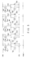
- the head driving device has the arrangement shown in FIG. 2 to drive the multi-nozzle ink-jet head as described above. More specifically, the equivalent circuit of the ink-jet head is a series circuit of capacitances W1, W2, W3, W4,--- constituted by piezoelectric elements W which are connected in series via the electrodes EL1, EL2, EL3, EL4, EL5,---.
- p-channel MOS field effect transistors TA1, TA2, TA3, TA4, TA5,--- serving as first semiconductor switching elements are connected between a VDD power supply terminal to which a VDD voltage is applied and the electrodes EL1, EL2, EL3, EL4, EL5,---, and n-channel MOS field effect transistors TB1, TB2, TB3, TB4, TB5,--- serving as second semiconductor switching elements are connected between a VSS power supply terminal to which a VSS voltage lower than the VDD voltage is applied and the electrodes EL1, EL2, EL3, EL4, EL5,---.
- the back gates of the p-channel MOS field effect transistors TA1, TA2, TA3, TA4, TA5,--- are connected to the VDD power supply terminal, and the back gates of the n-channel MOS field effect transistors TB1, TB2, TB3, TB4, TB5,--- are connected to a VSUB power supply terminal having a potential different from those of the VDD power supply terminal and the VSS power supply terminal.
- the VSUB potential of the VSUB power supply terminal is applied to the semiconductor substrate of the integrated circuit.
- a drive signal is supplied to the gate terminals of the field effect transistors TA1, TA2, TA3, TA4, TA5,--- through inverters IV1, IV2, IV3, IV4, IV5,---.
- the VDD potential is set to 20V
- the VSS potential is set to 0V
- the VSUB potential is set to -5V.
- a current rarely flows to the VSUB power supply terminal, and the VSUB power supply terminal does not require voltage precision. For this reason, -5V can be easily set by a charge pump or the like.
- the head driving device may be mounted on the ink-jet head along with such a charge pump circuit to reduce an amount of wiring.
- a low-level drive signal is supplied to the gate terminals of the field effect transistors TA1, TA2, TA3, TA4, TA5,--- through the inverters IV1, IV2, IV3, IV4, IV5,---, and the field effect transistors TA1, TA2, TA3, TA4, TA5,--- are set in an OFF state.
- a high-level drive signal is supplied to the gate terminals of the field effect transistors TB1, TB2, TB3, TB4, TB5,---, and the field effect transistors TB1, TB2, TB3, TB4, TB5,--- are set in an ON state.
- the capacitances W1, W2, W3, W4,--- are set in a discharge state.
- the state of the ink-jet head at this time is shown in FIG. 1A.
- a high-level drive signal is supplied to the gate of the field effect transistor TA3 through the inverter IV3 to turn on the field effect transistor TA3, and a low-level drive signal is supplied to the gate of the field effect transistor TB3 to turn off the field effect transistor TB3.
- a voltage of 20V is applied to electrode EL3 from the VDD power supply terminal to charge the capacitances W2 and W3.
- the charge path used at this time is as follows: VDD > transistor TA3 > electrode EL3 > capacitance W2 > electrode EL2 > transistor TB2 > VSS and VDD > transistor TA3 > electrode EL3 > capacitance W3 > electrode EL4 > transistor TB4 > VSS.
- the piezoelectric element W between the electrodes EL2 and EL3 and the piezoelectric element W between the electrode EL3 and EL4 are distorted externally when viewed from the ink chamber B to be set in the state of FIG. 1B.
- the state of the ink chamber B returns to the original state of FIG. 1A. In this manner, the state of the ink chamber B changes from the state of FIG. 1A to the state of FIG. 1B and returns to the state of FIG. 1A. As a result, ink is ejected from the nozzle of the ink chamber B.
- the terminals of the field effect transistors TB2 and TB4 on the VSS power supply terminal side serve as sources in charging, and serve as drains in discharging.
- the VSUB potential (-5V) lower than the VSS potential (0V) is applied to the back gates of the field effect transistors TB2 and TB4, and the back gates are isolated from the VSS potential.
- a voltage applied to the VSUB power supply terminal is set to be larger than a value obtained by subtracting a pn contact potential from a drop voltage generated by the field effect transistors TB2 and TB4 in discharging, no current from the semiconductor substrate is drawn to the field effect transistors TB2 and TB4. More specifically, when the VSS potential and the VSUB potential are set to 0V and -5V, the current from the semiconductor is not drawn.
- the driving device when the driving device is incorporated in the semiconductor substrate to form an IC, drawing of a current from the substrate potential does not occur. Therefore, when the driving device is mounted on an IC, the driving device is not easily influenced by parasitic active elements in the IC, and a head driving IC having high reliability can be obtained without causing degradation of inter-element isolation or latch up.
- wiring is desirably performed such that the drains of the adjacent field effect transistors TB1, TB2, TB3, TB4, TB5,--- are as close to each other as possible. Therefore, the loop of the discharge path in discharging can be decreased in size, and an influence of a rush current in discharging on the circuit can be reduced.
- the field effect transistors TB1, TB2, TB3, TB4, TB5,--- have bidirectional properties, diodes need not be parallel connected to the transistors to form a discharge path, thereby obtaining a simple circuit arrangement. Therefore, the driving device is mounted on an IC, an area occupied by the driving device can be advantageously decreased.
- a head driving device according to the second embodiment of the present invention will be described below.
- the potentials of the VSS power supply terminal and the VSUB power supply terminal are set to be equal to each other. More specifically, when a discharge current is small in the driving device in FIG. 2, voltage drop occurring in the field effect transistors TB2 and TB4 is small. On the other hand, a current does not flow between the semiconductor substrate and the electrodes EL2 and EL4 until a potential difference larger than the forward voltage of the pn contact is generated. More specifically, a discharge current does not flow through a parasitic diode formed between the semiconductor substrate and the electrodes EL2 and EL4.
- a head driving device according to the third embodiment of the present invention will be described below.
- diodes DX1, DX2, DX3, DX4, DX5,--- are parallel connected to field effect transistors TB1, TB2, TB3, TB4, TB5,--- to have reversed polarity. More specifically, the anodes of the diodes DX1, DX2, DX3, DX4, DX5,--- are commonly connected to the VSS power supply terminal, and the cathodes of the diodes DX1, DX2, DX3, DX4, DX5,--- are commonly connected to electrodes EL1, EL2, EL3, EL4, EL5,---.
- the head driving device is incorporated in the substrate to form an IC, drawing of a current from the substrate potential does not occur, and a head driving IC having high reliability can be structured.
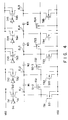
- a head driving device according to the fourth embodiment of the present invention will be described below.
- MOS transfer gates (a kind of transistor) TG1, TG2, TG3, TG4,--- serving as third semiconductor switching elements are connected in parallel with capacitances W1, W2, W3, W4,---. More specifically, the MOS transfer gate TG1 is connected between the electrodes EL1 and EL2, the MOS transfer gate TG2 is connected between the electrodes EL2 and EL3, the MOS transfer gate TG3 is connected between the electrodes EL3 and EL4, and the MOS transfer gate TG4 is connected to the electrodes EL4 and EL5.
- the field effect transistors TA1, TA2, TA3, TA4, TA5,.. are set in an OFF state
- the field effect transistors TB1, TB2, TB3, TB4, TB5,--- are set in an ON state
- the MOS transfer gates TG1, TG2, TG3, TG4,--- are set in an OFF state.
- the field effect transistors TA3 and TB3 are set in an OFF state, and the field effect transistors TB2 and TB4 are set in an ON state. For this reason, the potentials at all the points are not lower than the VSS voltage.
- the driving unit is mounted on an IC, drawing of a current from the substrate potential does not occur. Therefore, as in this embodiment, a head driving IC having high reliability can be structured.
- the MOS transfer gates TG2 and TG3 are turned on when charges for charging the capacitances W2 and W3 are discharged by a charge current flowing through the field effect transistor TA3.
- the MOS transfer gate TG2 is also turned on when reversely charges which charge the capacitance W2 are discharged by a charge current flowing through the field effect transistor TA2
- the MOS transfer gate TG4 is also turned on when charges which reversely charge the capacitance W3 are discharged by a charge current flowing through the field effect transistor TA4.
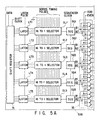
- FIGS. 5A and 5B are block diagrams showing the arrangement of an entire control section including the head driving device in FIG. 4.
- data to be printed are serially supplied to a shift register 31 and stored in the shift register 31 in synchronism with a shift clock.
- the data stored in the shift register 31 correspond to 4-bit gradation data for each nozzle, and the 4-bit gradation data are respectively latched by 4-bit latch circuits LT1, LT2, LT3, LT4, and LT5 by a latch pulse. After the data are latched, data to be printed next can be stored in the shift register 31.
- the 4-bit gradation data latched by the 4-bit latch circuits LT1, LT2, LT3, LT4, and LT5 are supplied to 16 to 1 selectors SL1, SL2, SL3, SL4, and SL5, respectively.
- the selectors SL1, SL2, SL3, SL4, and SL5 selects one from 16 timing pulse strings additionally input on the basis of the values of the input gradation data, to output the selected timing pulse string.
- the selected timing pulses are supplied to 2-bit sequencers SQ1, SQ2, SQ3, SQ4, and SQ5, respectively.
- One of the 16 timing pulse strings is non-signal data for non-printing.
- the remaining W timing pulse strings are set to be pulse strings which are preset to control the 2-bit sequencers SQ1, SQ2, SQ3, SQ4, and SQ5 at a timing by a procedure in which amounts of ink to be ejected are set depending on respective gradations.
- the 2-bit sequencers SQ1, SQ2, SQ3, SQ4, and SQ5 convert the input timing pulse into control timing data B1 and B2 including the information of the order and time of four states, i.e., "0,0", "0,1", “1,0", and "1,1" in synchronism with a sequencer clock.
- control timing data B1 and B2 from the sequencers SQ1, SQ2, SQ3, SQ4, and SQ5 are assigned to odd-number nozzles or even- number nozzles by a demultiplexer 35 constituted by a plurality of AND gates.
- the demultiplexer 35 supplies the control timing data B1 and B2 from the sequencers SQ1, SQ2, SQ3, SQ4, and SQ5 to decoders DCA1, DCA2, DCA3, DCA4, and DCA5 in response to an odd-number selection signal ODD, respectively, and the demultiplexer 35 supplies the control timing data Bl and B2 from the sequencers SQ1, SQ2, SQ3, SQ4, and SQ5 to decoders DCB1, DCB2, DCB3, DCB4, and DCB5 in response to an even-number selection signal EVEN, respectively.
- a signal "0,0" is supplied to the decoders DCB1, DCB2, DCB3, DCB4, and DCBS corresponding to the even-number nozzles when the odd-number selection signal ODD is input, and to the decoders DCA1, DCA2, DCA3, DCA4, and DCA5 corresponding to the odd-number nozzles when the even-number selection signal EVEN is input.
- the decoder DCA1 is constituted by three two-input AND gates DCA11, DCA12, and DCA13 and two inverters DCA14 and DCA15
- the decoder DCB1 is constituted by three two-input AND gates DCB11, DCB12, and DCB13 and two inverters DCB14 and DCB15.
- the decoder DCA1 directly inputs a signal A11 of two-bit signals A11 and A21 from the demultiplexer 35 to the AND gate DCA13, and inputs the signal A11 to the AND gates DCA11 and DCA12 through the inverter DCA14.
- the decoder DCA1 directly inputs the signal A21 to the AND gates DCA11 and DCA13, and inputs the signal A21 to the AND gate DCA12 through the inverter DCA15.
- the decoder DCB1 directly inputs a signal A12 of two-bit signals A12 and A22 from the demultiplexer 35 to the AND gate DCB13, and inputs the signal A12 to the AND gates DCB11 and DCB12 through the inverter DCB14.
- the decoder DCB1 directly inputs the signal A22 to the AND gates DCB11 and DCB13, and inputs the signal A22 to the AND gate DCB12 through the inverter DCB15.
- a drive signal is supplied from the AND gates DCA11, DCA12, DCA13, DCB11, DCB12, and DCB13 to a head driving device 38.
- the head driving device 38 comprises transistor circuit sections TCA1 to TCA10, OR gates G1 to G9, and transistor circuit sections TCB1 to TCB9.
- the transistor circuit sections TCA1 to TCA10 have the field effect transistors TA1, TB1, TA2, TB2, TA3, TB3, TA4, TB4, TA5, TB5,--- and the inverters IV1, IV2, IV3, IV4, IV5,--- shown in FIG. 4.
- the transistor circuit sections TCB1 to TCB9 have the MOS transfer gates TG1, TG2, TG3, TG4,--- shown in FIG. 4.
- a drive signal S11 is supplied from the AND gate DCA11 of the decoder DCA1 to the inverter IV1 of the transistor circuit section TCA1, and a drive signal S21 is supplied from the AND gate DCA12 to the gate of the field effect transistor TB1 of the transistor circuit section TCA1.
- a drive signal S31 is output from the AND gate DCA13, and the drive signal S31 is supplied as a drive signal S1-2 to the gate of the MOS transfer gate TG1 of the transistor circuit section TCB1 through the OR gate G1.
- a drive signal S12 is supplied from the AND gate DCB11 of the decoder DCB1 to the inverter IV2 of the transistor circuit section TCA2, and a drive signal S22 is supplied from the AND gate DCB12 to the gate of the field effect transistor TB2 of the transistor circuit section TCA2.
- a drive signal S32 is output from the AND gate DCB13, and the drive signal S32 is supplied as a drive signal S1-2 to the gate of the MOS transfer gate TG1 of the transistor circuit section TCB1 through the OR gate G1, and is supplied as a drive signal S2-3 to the gate of the MOS transfer gate TG2 of the transistor circuit section TCB2 through the OR gate G2.
- the output terminals of the transistor circuit sections TCA1 to TCA10 are connected to electrodes EL1 to EL10 connected to capacitances W1 to W9, respectively.
- the input/output relationship among the decoders DCA1 to DCA5 and DCB1 to DCBS is expressed by a truth table, and the output states of the head driving device 38 corresponding to the truth table are shown in the following table: Table 1 A1 A2 S1X S2X S3X OUTPUT 0 0 L H L VSS VOLTAGE 0 1 H L L VDD VOLTAGE 1 0 H L L OFF 1 1 L L H SHORT-CIRCUIT LOOP
- Symbol A1 indicates the signals A11, A12,---, and symbol A2 indicates the signals A21, A22,---.
- Symbol S1X indicates the drive signals S11, S12,---, symbol S2X indicates the drive signals S21, S22,---, and symbol S3X indicates the drive signals S31, S32,---.
- 4-bit gradation data for driving odd-number nozzles i.e., (odd-number)th ink chambers
- the latched gradation data are supplied to the 16 to 1 selectors SL1 to SL5 to be converted into one timing pulse.
- the timing pulses from the selectors SL1 to SL5 are supplied to the 2-bit sequencers SQ1 to SQ5, respectively, to be converted into control timing data B1 and B2.
- the control timing data B1 and B2 from the sequencers SQ1 to SQ5 are supplied to the demultiplexer 35.
- the demultiplexer 35 supplies the control timing data B1 and B2 from the sequencers SQ1 to SQ5 to the decoders DCA1 to DCA5 corresponding to the odd-number nozzles, respectively.
- the transistor circuit sections TCA1, TCA3, TCA5, TCA7, and TCA9 and the transistor circuit sections TCB1 to TCB9 are selectively driven by signals from the decoders DCA1 to DCA5. In this manner, the capacitances W1 to W9 are selectively charge/discharge-controlled, and the piezoelectric elements constituting the partition walls of the ink chambers are distorted to give pressures to desired ink chambers, thereby ejecting predetermined amounts of ink depending on the gradation data.
- the second and fourth nozzles adjacent to the third nozzle are (even-number)th nozzles which are not assigned.
- ink is ejected from the ink chamber corresponding to the third nozzle, and no ink is ejected from the ink chambers adjacent to the third nozzle.
- the (odd-number)th nozzles and the (even-number)th nozzles are alternately driven to perform printing.
- a head driving device according to the fifth embodiment of the present invention will be described below.
- another driving method is realized by using the driving device shown in FIG. 4 as in the fourth embodiment.
- this head driving device in a stationary state, field effect transistors TA1, TA2, TA3, TA4, TA5,--- are set in an OFF state, field effect transistors TB1, TB2, TB3, TB4, TB5,--- are set in an OFF state, and MOS transfer gates TG1, TG2, TG3, TG4,--- are set in an ON state.
- the field effect transistors TA3, TB2, and TB4 are turned off, and the field effect transistors TA2, TA4, and TB3 are turned on. In this manner, the capacitances W2 and W3 are reversely charged.
- a charge path used at this time is as follows: VDD > transistor TA2 > electrode EL2 > capacitance W2 > electrode EL3 > transistor TB3 > VSS and VDD > transistor TA4 > electrode EL4 > capacitance W3 > electrode EL3 > transistor TB3 > VSS.
- ink chamber B are compressed as shown in FIG. 1C to eject ink from nozzles.
- ink ejection is performed during reverse charging, and then, discharging is performed. Therefore, the following method may be effective to prevent erroneous ejection. That is, discharging is slowly performed depending on conditions such as the properties of ink such that the discharging rate is not extremely high, thereby suppressing an abrupt change in ink pressure.
- the ON resistance of the MOS transfer gates TG1 to TG4 may be set to be high, and a time constant determined by the capacitances W1 to W4 and the ON resistance of the MOS transfer gates TG1 to TG4 may be set to be large.
- the present invention is not limited to these embodiments, and, as shown in FIGS. 7A to 7C, a head in which piezoelectric elements W constituting partition walls are polarized in the lower direction may be used. In this case, in contrast to the case shown in FIG. 1, as shown in FIG.
- a piezoelectric element is used as an electrostrictive element.
- the piezoelectric element is not limited to the electrostrictive element.
- An electrostrictive element using electrostatic force may be used.
- the electrostrictive element directly constitutes the wall surface of an ink chamber.
- the present invention is not limited to this arrangement, and an electrostrictive element may indirectly distort the wall surface of the ink chamber. In short, the pressure in an ink chamber may be only changed by electrostriction of the electrostrictive element.
- a head in which electrostrictive elements are different in mechanical structure, but constitute capacitances connected in series with each other can be used.
Abstract


Description
- The present invention relates to a head driving device for an ink-jet printer having an ink-jet head which utilizes electrostrictive elements for causing variations in pressure in ink chambers by electrostriction thereof.
- The head of an ink-jet printer of this type has, e.g., an arrangement shown in FIG. 8. More specifically, a plurality of recessed grooves are formed in a
piezoelectric member 1 at predetermined pitches, and anupper lid 2 is fixed on the grooves to formink chambers 3 in association with the grooves. Anelectrode 4 is spread over the bottom portion and side walls of eachink chamber 3. A nozzle (not shown) is formed in front of eachink chamber 3, and an ink supply port (not shown) is formed in the rear of eachink chamber 3. In this head, thepiezoelectric member 1 has portions forming walls for partitioning theink chambers 3 from each other and serving aspiezoelectric elements 5 interposed betweenelectrodes 4. For this reason, adjacent two of theelectrodes 4 constitutes a capacitance along with thepiezoelectric element 5 located therebetween. Accordingly, the equivalent circuit of this head may be expressed by a series circuit of capacitors connected to each other via theelectrodes 4. - A head driving device for driving such a head is disclosed in Japanese Unexamined Patent Publication No. 2-18054. For example, as shown in FIG. 9, the equivalent circuit of the head is a series circuit of capacitances CL1, CL2, CL3, CL4,--- connected in series and constituted by
piezoelectric elements 5 and electrodes a, b, c, d, e,---. For this circuit, p-channel MOS field effect transistors Q11, Q12, Q13, Q14, Q15,--- are connected between a VDD power supply terminal and the electrodes a, b, c, d, e,---, and n-channel MOS field effect transistors Q21, Q22, Q23, Q24, Q25,--- are connected between a ground line and the electrodes a, b, c, d, e,---. - Diodes Dl, D2, D3, D4, D5,--- are connected in parallel with the n- channel MOS field effect transistors Q21, Q22, Q23, Q24, Q25,--- to have reversed polarity. The back gates of the p-channel MOS field effect transistors Q11, Q12, Q13, Q14, Q15,--- are connected to the VDD power supply terminal, and the back gates of the n-channel MOS field effect transistors Q21, Q22, Q23, Q24, Q25,--- are connected to the ground line. Drive signals are supplied to the gate terminals of the field effect transistors Q11, Q12, Q13, Q14, Q15,--- through inverters IN1, IN2, IN3, IN4, IN5,---. In this driving device, for example, when the electrode c is energized, a drive signal is supplied to the gate terminal of the field effect transistor Q13 through the inverter IN3 to turn on the transistor Q13. The field effect transistors Q22 and Q24 are also turned on. At this time, a charge current flows through a path: VDD > transistor Q13 > capacitance CL2 > transistor Q22 > ground line, and a charge current flows through a path: VDD > transistor Q13 > capacitance CL3 > transistor Q24 > ground line, thereby charging the capacitances CL2 and CL3. When the capacitances CL2 and CL3 are to be discharged, the field effect transistors Q13, Q22, and Q24 are turned off, and the field effect transistor Q23 is turned on. At this time, a discharge current flows through a path: ground line > diode D2 > capacitance CL2 > transistor Q23 > ground line, and a discharge current flows through a path: ground line > diode D4 > capacitance CL3 > transistor Q23 > ground line, thereby discharging the capacitances CL2 and CL3.
- With the charging and discharging, the piezoelectric element between the electrodes b and c and the piezoelectric element between the electrodes c and d are distorted. Since an ink chamber is temporarily expanded and then returns to the original state, ink in the ink chamber is ejected via the nozzle by a pressure applied thereto.
- When such a head driving device is incorporated in a semiconductor substrate to be an IC (integrated circuit), the following problem is raised. More specifically, since the diodes D2 and D4 are turned on in discharging, the voltages of the electrodes b and d are lower than the ground potential by a forward voltage drop across a PN contact. In this case, since parasitic diodes are formed between the electrodes b and d and the back gates of the field effect transistors Q22 and Q24, part of the discharge current also flow in both the parasitic diodes. The reliability of the IC is degraded due to the currents which flow in the semiconductor substrate. In addition, inter-element isolation is degraded, and, in the worst case, latch up may occur.
- It is an object of the present invention to provide a head driving device for an ink-jet printer, which can be manufactured as a reliable IC which is not easily influenced by a parasitic active element created therein, and does not cause degradation of inter-element isolation and latch up.
- According to the first aspect of the present invention, there is provided a head driving device for an ink-jet printer, comprising an ink-jet head having a plurality of ink chambers, electrodes for the respective ink chambers, and electrostrictive elements which are arranged to separate the ink chambers and form a series of capacitances connected by the electrodes and which cause variations in pressure in the ink chambers by electrostriction, electrodes for the respective ink chambers, a plurality of first semiconductor switching elements connected between a first power supply terminal and the electrodes, and a plurality of second semiconductor switching elements connected between the electrodes and a second power supply terminal having a potential different from that of the first power supply terminal, wherein ink is ejected from each ink chamber due to the variation in pressure which is caused by charging and discharging of corresponding capacitances under a control of selectively turning on the first and second semiconductor switching elements; both of the first semiconductor switching elements and second semiconductor switching elements are formed on one semiconductor substrate; and the potential of the semiconductor substrate is set to be out of a range between the potentials of the first and second power supply terminals.
- According to the second aspect of the present invention, there is provided a head driving device for an ink-jet printer, comprising an ink-jet head having a plurality of ink chambers, electrodes for the respective ink chambers, and electrostrictive elements which are arranged to separate the ink chambers and form a series of capacitances connected by the electrodes and which cause variations in pressure in the ink chambers by electrostriction, electrodes for the respective ink chambers, a plurality of first semiconductor switching elements connected between a first power supply terminal and the electrodes, and a plurality of second semiconductor switching elements connected between the electrodes and a second power supply terminal having a potential lower than that of the first power supply terminal, wherein ink is ejected from a predetermined ink chamber due to the variation in pressure which is caused by charging and discharging of two capacitances each across the electrode for the predetermined ink chamber and the electrodes for a corresponding ink chamber adjacent to the predetermined ink chamber under a charging control of turning on and off the respective first and second semiconductor switching elements connected to the electrode for a predetermined ink chamber and turning off and on the respective first and second semiconductor switching elements connected to the electrodes of the ink chambers adjacent to the predetermined ink chamber, and a subsequent discharging control of turning off and on the respective first and second semiconductor switching elements connected to the electrode for a predetermined ink chamber, both of the first semiconductor switching elements and second semiconductor switching elements are formed on one semiconductor substrate; and the potential of the semiconductor substrate is set to be out of a range between the potentials of the first and second power supply terminals.
- According to the third aspect of the present invention, there is provided a head driving device for an ink-jet printer, comprising an ink-jet head having a plurality of ink chambers, electrodes for the respective ink chambers, and electrostrictive elements which are arranged to separate the ink chambers and form a series of capacitances connected by the electrodes and which cause variations in pressure in the ink chambers by electrostriction, electrodes for the respective ink chambers, a plurality of first semiconductor switching elements connected between a first power supply terminal and the electrodes, and a plurality of second semiconductor switching elements connected between the electrodes and a second power supply terminal having a potential different from that of the first power supply terminal, wherein ink is ejected from each ink chamber due to the variation in pressure which is caused by charging and discharging of corresponding capacitances under a control of selectively turning on the first and second semiconductor switching elements; at least one of groups of the first semiconductor switching elements and second semiconductor switching elements are constituted by MOS transistors formed on an integrated circuit; and the potential of a back gate of each MOS transistor is set to be out of a range between the potentials of a source and drain of the MOS transistor.
- According to the fourth aspect of the present invention, there is provided a head driving device for an ink-jet printer, comprising an ink-jet head having a plurality of ink chambers, electrodes for the respective ink chambers, and electrostrictive elements which are arranged to separate the ink chambers and form a series of capacitances connected by the electrodes and which cause variations in pressure in the ink chambers by electrostriction, electrodes for the respective ink chambers, a plurality of first semiconductor switching elements connected between a first power supply terminal and the electrodes, and a plurality of second semiconductor switching elements connected between the electrodes and a second power supply terminal having a potential lower than that of the first power supply terminal, wherein ink is ejected from a predetermined ink chamber due to the variation in pressure which is caused by charging and discharging of two capacitances each across the electrode for the predetermined ink chamber and the electrodes for a corresponding ink chamber adjacent to the predetermined ink chamber under a charging control of turning on and off the respective first and second semiconductor switching elements connected to the electrode for a predetermined ink chamber and turning off and on the respective first and second semiconductor switching elements connected to the electrodes of the ink chambers adjacent to the predetermined ink chamber, and a subsequent discharging control of turning off and on the respective first and second semiconductor switching elements connected to the electrode for a predetermined ink chamber, at least one of groups of the first semiconductor switching elements and second semiconductor switching elements is constituted by MOS transistors formed on an integrated circuit; and the potential of a back gate of each MOS transistor is set to be out of a range between the potentials of a source and drain of the MOS transistor.
- According to the fifth aspect of the present invention, there is provided a head driving device for an ink-jet printer, comprising an ink-jet head having a plurality of ink chambers, electrodes for the respective ink chambers, and electrostrictive elements which are arranged to separate the ink chambers and form a series of capacitances connected by the electrodes and which cause variations in pressure in the ink chambers by electrostriction, electrodes for the respective ink chambers, a plurality of first semiconductor switching elements connected between a first power supply terminal and the electrodes, and a plurality of second semiconductor switching elements connected between the electrodes and a second power supply terminal having a potential different from that of the first power supply terminal, wherein ink is ejected from each ink chamber due to the variation in pressure which is caused by charging and discharging of corresponding capacitances under a control of selectively turning on the first and second semiconductor switching elements; at least the second semiconductor switching elements are constituted by MOS transistors, the capacitances are discharged through the MOS transistors which are turned on by an identical potential applied to the gates thereof.
- According to the sixth aspect of the present invention, there is provided a head driving device for an ink-jet printer, comprising an ink-jet head having a plurality of ink chambers, electrodes for the respective ink chambers, and electrostrictive elements which are arranged to separate the ink chambers and form a series of capacitances connected by the electrodes and which cause variations in pressure in the ink chambers by electrostriction, electrodes for the respective ink chambers, a plurality of first semiconductor switching elements connected between a first power supply terminal and the electrodes, a plurality of second semiconductor switching elements connected between the electrodes and a second power supply terminal having a potential different from that of the first power supply terminal, and a plurality of third semiconductor switching elements each connected between adjacent two electrodes, wherein ink is ejected from each ink chamber due to the variation in pressure which is caused by charging and discharging of corresponding capacitances under a charging and discharging control of selectively turning on the first and second semiconductor switching elements and a discharging control of selectively turning on the third semiconductor switching elements.
- According to the seventh aspect of the present invention, there is provided a head driving device for an ink-jet printer, comprising an ink-jet head having a plurality of ink chambers, electrodes for the respective ink chambers, and electrostrictive elements which are arranged to separate the ink chambers and form a series of capacitances connected by the electrodes and which cause variations in pressure in the ink chambers by electrostriction, electrodes for the respective ink chambers, a plurality of first semiconductor switching elements connected between a first power supply terminal and the electrodes, a plurality of second semiconductor switching elements connected between the electrodes and a second power supply terminal having a potential lower than that of the first power supply terminal, and a plurality of third semiconductor switching elements each connected between adjacent two electrodes, wherein ink is ejected from a predetermined ink chamber due to the variation in pressure which is caused by charging and discharging of two capacitances each across the electrode for the predetermined ink chamber and the electrode for a corresponding ink chamber adjacent to the predetermined ink chamber under a charging control of turning on and off the respective first and second semiconductor switching elements connected to the electrode for a predetermined ink chamber, turning off and on the respective first and second semiconductor switching elements connected to the electrodes of the ink chambers adjacent to the predetermined ink chamber, and turning off the third semiconductor switching elements connected between the adjacent two electrodes, and a subsequent discharging control of turning off the respective first semiconductor switching element connected to the electrode for a predetermined ink chamber, and turning on the third semiconductor switching elements connected between the adjacent two electrodes.
- According to the eighth aspect of the present invention, there is provided a head driving device for an ink-jet printer which has the same arrangement as that of the head driving device provide according to the sixth or seventh aspect, wherein the third semiconductor switching elements are constituted by MOS transfer gates.
- Each of the head driving devices according to the first to eighth aspects can be manufactured as a reliable IC which is not easily influenced by a parasitic active element created therein, and does not cause degradation of inter-element isolation and latch up.
- In the head driving device according to the fifth aspect, since no diode is used in the discharge path, the circuit configuration can be simplified.
- In each of the head driving devices according to the sixth to eighth aspects, furthermore, the loop resistance of the discharge path can be decreased, and the head can be operated at a high speed.
- In each of the head driving devices according to the sixth and eighth aspects, furthermore, erroneous ejection of ink can be prevented by decreasing the discharging speed of the capacitance.
- This invention can be more fully understood from the following detailed description when taken in conjunction with the accompanying drawings, in which:
- FIGS. 1A to 1C are sectional views for explaining operations of a multi-nozzle ink-jet head used in each embodiment of the present invention;
- FIG. 2 is a circuit diagram showing the arrangement of a head driving device according to the first embodiment of the present invention;
- FIG. 3 is a circuit diagram showing the arrangement of a head driving device according to the third embodiment of the present invention;
- FIG. 4 is a circuit diagram showing the arrangement of a head driving device according to the fourth embodiment of the present invention;
- FIGS. 5A and 5B are block diagrams showing the arrangement of an entire control section using the head driving device according to the fourth embodiment;
- FIG. 6 is a circuit diagram of a decoder shown in FIG. 5B;
- FIGS. 7A to 7C are sectional views showing another arrangement of a multi-nozzle ink-jet head used in each embodiment of the present invention;
- FIG. 8 is a sectional view showing the arrangement of a typical multi-nozzle ink-jet head; and
- FIG. 9 is a circuit diagram showing the arrangement of a conventional head driving device.
- A head driving device according to the first embodiment of the present invention will be described below.
- FIG. 1 shows the arrangement of a multi-nozzle ink-jet head. A plurality of recessed grooves are formed in a
piezoelectric member 11 at predetermined pitches, and anupper lid 12 is fixed on the grooves to form ink chambers RM in association with the grooves. An electrode EL is spread over the bottom portion and side walls of each ink chamber RM. A nozzle (not shown) is formed in front of each ink chamber RM, and an ink supply port (not shown) is formed in the rear of each ink chamber RM. In this head, thepiezoelectric member 11 has portions forming walls which separate the ink chambers RM from each other and serve as piezoelectric (or electrostrictive) elements W interposed between the electrodes EL. The respective piezoelectric elements W are polarized upward as indicated by arrows in FIGS. 1A to 1C. - In this ink-jet head, the electrodes EL are normally grounded as shown in FIG. 1A. When a positive voltage is applied to a selected electrode EL as shown in FIG. 1B, two piezoelectric elements W between the selected electrode EL and the electrodes EL adjacent thereto are externally distorted to expand the ink chamber RM in which the selected electrode EL is present. In contrast to this, as shown in FIG. lC, when a negative voltage is applied to the selected electrode EL, the two piezoelectric elements W between the selected electrode EL and the electrodes EL adjacent thereto are internally distorted to compress the ink chamber RM in which the selected electrode EL is present. Therefore, in the ink-jet head, when the state of the ink chamber RM is changed into two or more states (of the three states show in FIGS. 1A, 1B, and 1C) including at least the state shown in FIG. lA, ink can be ejected from the nozzle (orifice surface). The amount, speed, shape, stability, and the like of ejected ink droplets are determined depending on a combination among the order, duration, and rate of the change of three states shown in FIGS. 1A, 1B, and 1C and an amount of distortion. In general, these conditions are optimized by experiments. In addition, the driving conditions are adjusted to change the amount, speed, shape, stability, and the like of ink droplets, if it is necessary to obtain gradations or compensate for differences between the characteristics of paper, ink, a head, or the like.
- The head driving device has the arrangement shown in FIG. 2 to drive the multi-nozzle ink-jet head as described above. More specifically, the equivalent circuit of the ink-jet head is a series circuit of capacitances W1, W2, W3, W4,--- constituted by piezoelectric elements W which are connected in series via the electrodes EL1, EL2, EL3, EL4, EL5,---.
- With this circuit, p-channel MOS field effect transistors TA1, TA2, TA3, TA4, TA5,--- serving as first semiconductor switching elements are connected between a VDD power supply terminal to which a VDD voltage is applied and the electrodes EL1, EL2, EL3, EL4, EL5,---, and n-channel MOS field effect transistors TB1, TB2, TB3, TB4, TB5,--- serving as second semiconductor switching elements are connected between a VSS power supply terminal to which a VSS voltage lower than the VDD voltage is applied and the electrodes EL1, EL2, EL3, EL4, EL5,---. The back gates of the p-channel MOS field effect transistors TA1, TA2, TA3, TA4, TA5,--- are connected to the VDD power supply terminal, and the back gates of the n-channel MOS field effect transistors TB1, TB2, TB3, TB4, TB5,--- are connected to a VSUB power supply terminal having a potential different from those of the VDD power supply terminal and the VSS power supply terminal. When the field effect transistors TA1, TA2, TA3, TA4, TA5,--- and the field effect transistors TB1, TB2, TB3, TB4, TB5,--- are incorporated in a semiconductor substrate (shown later as SUB) to constitute the integrated circuit, the VSUB potential of the VSUB power supply terminal is applied to the semiconductor substrate of the integrated circuit.
- A drive signal is supplied to the gate terminals of the field effect transistors TA1, TA2, TA3, TA4, TA5,--- through inverters IV1, IV2, IV3, IV4, IV5,---.
- In this head driving device, for example, the VDD potential is set to 20V, the VSS potential is set to 0V, and the VSUB potential is set to -5V. A current rarely flows to the VSUB power supply terminal, and the VSUB power supply terminal does not require voltage precision. For this reason, -5V can be easily set by a charge pump or the like. More specifically, the head driving device may be mounted on the ink-jet head along with such a charge pump circuit to reduce an amount of wiring.
- For example, a case wherein an ink is ejected from an ink chamber B will be described below. In a stationary state, a low-level drive signal is supplied to the gate terminals of the field effect transistors TA1, TA2, TA3, TA4, TA5,--- through the inverters IV1, IV2, IV3, IV4, IV5,---, and the field effect transistors TA1, TA2, TA3, TA4, TA5,--- are set in an OFF state. A high-level drive signal is supplied to the gate terminals of the field effect transistors TB1, TB2, TB3, TB4, TB5,---, and the field effect transistors TB1, TB2, TB3, TB4, TB5,--- are set in an ON state. In this manner, the capacitances W1, W2, W3, W4,--- are set in a discharge state. The state of the ink-jet head at this time is shown in FIG. 1A.
- In this state, a high-level drive signal is supplied to the gate of the field effect transistor TA3 through the inverter IV3 to turn on the field effect transistor TA3, and a low-level drive signal is supplied to the gate of the field effect transistor TB3 to turn off the field effect transistor TB3. In this manner, a voltage of 20V is applied to electrode EL3 from the VDD power supply terminal to charge the capacitances W2 and W3. The charge path used at this time is as follows: VDD > transistor TA3 > electrode EL3 > capacitance W2 > electrode EL2 > transistor TB2 > VSS and VDD > transistor TA3 > electrode EL3 > capacitance W3 > electrode EL4 > transistor TB4 > VSS.
- With this charging, the piezoelectric element W between the electrodes EL2 and EL3 and the piezoelectric element W between the electrode EL3 and EL4 are distorted externally when viewed from the ink chamber B to be set in the state of FIG. 1B.
- In this state, when the field effect transistor TA3 is turned off, and the field effect transistor TB3 is turned on, the capacitances W2 and W3 are discharged. A discharge path used at this time is as follows: VSS > transistor TB2 > electrode EL2 > capacitance W2 > electrode EL3 > transistor TB3 > VSS and VSS > transistor TB4 > electrode EL4 > capacitance W3 > electrode EL3 > transistor TB3 > VSS.
- With this discharging, the state of the ink chamber B returns to the original state of FIG. 1A. In this manner, the state of the ink chamber B changes from the state of FIG. 1A to the state of FIG. 1B and returns to the state of FIG. 1A. As a result, ink is ejected from the nozzle of the ink chamber B.
- The terminals of the field effect transistors TB2 and TB4 on the VSS power supply terminal side serve as sources in charging, and serve as drains in discharging. The VSUB potential (-5V) lower than the VSS potential (0V) is applied to the back gates of the field effect transistors TB2 and TB4, and the back gates are isolated from the VSS potential. For this reason, when a voltage applied to the VSUB power supply terminal is set to be larger than a value obtained by subtracting a pn contact potential from a drop voltage generated by the field effect transistors TB2 and TB4 in discharging, no current from the semiconductor substrate is drawn to the field effect transistors TB2 and TB4. More specifically, when the VSS potential and the VSUB potential are set to 0V and -5V, the current from the semiconductor is not drawn.
- In this manner, when the driving device is incorporated in the semiconductor substrate to form an IC, drawing of a current from the substrate potential does not occur. Therefore, when the driving device is mounted on an IC, the driving device is not easily influenced by parasitic active elements in the IC, and a head driving IC having high reliability can be obtained without causing degradation of inter-element isolation or latch up.
- In the lines of the VSS power supply terminal, wiring is desirably performed such that the drains of the adjacent field effect transistors TB1, TB2, TB3, TB4, TB5,--- are as close to each other as possible. Therefore, the loop of the discharge path in discharging can be decreased in size, and an influence of a rush current in discharging on the circuit can be reduced.
- In this embodiment, since the field effect transistors TB1, TB2, TB3, TB4, TB5,--- have bidirectional properties, diodes need not be parallel connected to the transistors to form a discharge path, thereby obtaining a simple circuit arrangement. Therefore, the driving device is mounted on an IC, an area occupied by the driving device can be advantageously decreased.
- A head driving device according to the second embodiment of the present invention will be described below.
- In this embodiment, although the driving device shown in FIG. 2 having the same arrangement as that in the first embodiment is used, the potentials of the VSS power supply terminal and the VSUB power supply terminal are set to be equal to each other. More specifically, when a discharge current is small in the driving device in FIG. 2, voltage drop occurring in the field effect transistors TB2 and TB4 is small. On the other hand, a current does not flow between the semiconductor substrate and the electrodes EL2 and EL4 until a potential difference larger than the forward voltage of the pn contact is generated. More specifically, a discharge current does not flow through a parasitic diode formed between the semiconductor substrate and the electrodes EL2 and EL4.
- Therefore, when the discharge current is small, and voltage drop occurring in the field effect transistors TB2 and TB4 is sufficiently small, a discharge current does not flow in the semiconductor substrate even if VSS = VSUB is established. Under this condition, when VSS = VSUB is set, the number of types of power supplies can be decreased, and a simple structure can be obtained.
- A head driving device according to the third embodiment of the present invention will be described below.
- The same reference numerals as in the first embodiment described above denote the same parts in the third embodiment, and a description thereof will be omitted. According to this embodiment, as shown in FIG. 3, diodes DX1, DX2, DX3, DX4, DX5,--- are parallel connected to field effect transistors TB1, TB2, TB3, TB4, TB5,--- to have reversed polarity. More specifically, the anodes of the diodes DX1, DX2, DX3, DX4, DX5,--- are commonly connected to the VSS power supply terminal, and the cathodes of the diodes DX1, DX2, DX3, DX4, DX5,--- are commonly connected to electrodes EL1, EL2, EL3, EL4, EL5,---.
- In this manner, when the diodes DX1, DX2, DX3, DX4, DX5,--- are parallel connected to the field effect transistors TB1, TB2, TB3, TB4, TB5,---, the head can be operated at a high speed. More specifically, the ON resistance of the field effect transistors TB1, TB2, TB3, TB4, TB5,--- is generally higher than the ON resistance of the diodes DX1, DX2, DX3, DX4, DX5,---. Therefore, when the diodes DX1, DX2, DX3, DX4, DX5,--- are arranged on the discharge path of capacitances W1, W2, W3, W4,---, discharging is performed at a high speed, and the head can be operated at a high speed. In this case, the head driving device is incorporated in the substrate to form an IC, drawing of a current from the substrate potential does not occur, and a head driving IC having high reliability can be structured.
- A head driving device according to the fourth embodiment of the present invention will be described below.
- The same reference numerals as in the first embodiment described above denote the same parts in the fourth embodiment, and a description thereof will be omitted. According to this embodiment, as shown in FIG. 4, MOS transfer gates (a kind of transistor) TG1, TG2, TG3, TG4,--- serving as third semiconductor switching elements are connected in parallel with capacitances W1, W2, W3, W4,---. More specifically, the MOS transfer gate TG1 is connected between the electrodes EL1 and EL2, the MOS transfer gate TG2 is connected between the electrodes EL2 and EL3, the MOS transfer gate TG3 is connected between the electrodes EL3 and EL4, and the MOS transfer gate TG4 is connected to the electrodes EL4 and EL5.
- In this head driving device, in an stationary state, the field effect transistors TA1, TA2, TA3, TA4, TA5,.. are set in an OFF state, the field effect transistors TB1, TB2, TB3, TB4, TB5,--- are set in an ON state, and the MOS transfer gates TG1, TG2, TG3, TG4,--- are set in an OFF state.
- In this state, when the field effect transistor TA3 is turned on, and the field effect transistor TB3 is turned off, the capacitances W2 and W3 are charged. A charge path used at this time is as follows: VDD > transistor TA3 > electrode EL3 > capacitance W2 > electrode EL2 > transistor TB2 > VSS and VDD > transistor TA3 > electrode EL3 > capacitance W3 > electrode EL4 > transistor TB4 > VSS.
- In this state, when the field effect transistor TA3 is turned off, and the MOS transfer gates TG2 and TG3 are turned on, the capacitance W2 is discharged through the MOS transfer gate TG2, and the capacitance W3 is discharged through the MOS transfer gate TG2. In this manner, when the capacitances W2 and W3 are charged/discharged, ejection of ink is performed.
- When the capacitances W2 and W3 are discharged, the field effect transistors TA3 and TB3 are set in an OFF state, and the field effect transistors TB2 and TB4 are set in an ON state. For this reason, the potentials at all the points are not lower than the VSS voltage. When the driving unit is mounted on an IC, drawing of a current from the substrate potential does not occur. Therefore, as in this embodiment, a head driving IC having high reliability can be structured.
- In this driving device, since one capacitance is discharged by using only one MOS transfer gate, a charge path can be more shortened. Therefore, even if an ON resistance per transistor does not change, the loop resistance of the discharge path can be decreased, and the head can be operated at a high speed.
- As described above, the MOS transfer gates TG2 and TG3 are turned on when charges for charging the capacitances W2 and W3 are discharged by a charge current flowing through the field effect transistor TA3. However, the MOS transfer gate TG2 is also turned on when reversely charges which charge the capacitance W2 are discharged by a charge current flowing through the field effect transistor TA2, and the MOS transfer gate TG4 is also turned on when charges which reversely charge the capacitance W3 are discharged by a charge current flowing through the field effect transistor TA4.
- FIGS. 5A and 5B are block diagrams showing the arrangement of an entire control section including the head driving device in FIG. 4. In the control section, data to be printed are serially supplied to a
shift register 31 and stored in theshift register 31 in synchronism with a shift clock. The data stored in theshift register 31 correspond to 4-bit gradation data for each nozzle, and the 4-bit gradation data are respectively latched by 4-bit latch circuits LT1, LT2, LT3, LT4, and LT5 by a latch pulse. After the data are latched, data to be printed next can be stored in theshift register 31. - The 4-bit gradation data latched by the 4-bit latch circuits LT1, LT2, LT3, LT4, and LT5 are supplied to 16 to 1 selectors SL1, SL2, SL3, SL4, and SL5, respectively. The selectors SL1, SL2, SL3, SL4, and SL5 selects one from 16 timing pulse strings additionally input on the basis of the values of the input gradation data, to output the selected timing pulse string. The selected timing pulses are supplied to 2-bit sequencers SQ1, SQ2, SQ3, SQ4, and SQ5, respectively. One of the 16 timing pulse strings is non-signal data for non-printing. The remaining W timing pulse strings are set to be pulse strings which are preset to control the 2-bit sequencers SQ1, SQ2, SQ3, SQ4, and SQ5 at a timing by a procedure in which amounts of ink to be ejected are set depending on respective gradations. The 2-bit sequencers SQ1, SQ2, SQ3, SQ4, and SQ5 convert the input timing pulse into control timing data B1 and B2 including the information of the order and time of four states, i.e., "0,0", "0,1", "1,0", and "1,1" in synchronism with a sequencer clock. The control timing data B1 and B2 from the sequencers SQ1, SQ2, SQ3, SQ4, and SQ5 are assigned to odd-number nozzles or even- number nozzles by a
demultiplexer 35 constituted by a plurality of AND gates. More specifically, thedemultiplexer 35 supplies the control timing data B1 and B2 from the sequencers SQ1, SQ2, SQ3, SQ4, and SQ5 to decoders DCA1, DCA2, DCA3, DCA4, and DCA5 in response to an odd-number selection signal ODD, respectively, and thedemultiplexer 35 supplies the control timing data Bl and B2 from the sequencers SQ1, SQ2, SQ3, SQ4, and SQ5 to decoders DCB1, DCB2, DCB3, DCB4, and DCB5 in response to an even-number selection signal EVEN, respectively. Note that a signal "0,0" is supplied to the decoders DCB1, DCB2, DCB3, DCB4, and DCBS corresponding to the even-number nozzles when the odd-number selection signal ODD is input, and to the decoders DCA1, DCA2, DCA3, DCA4, and DCA5 corresponding to the odd-number nozzles when the even-number selection signal EVEN is input. - As shown in FIG. 6, the decoder DCA1 is constituted by three two-input AND gates DCA11, DCA12, and DCA13 and two inverters DCA14 and DCA15, and the decoder DCB1 is constituted by three two-input AND gates DCB11, DCB12, and DCB13 and two inverters DCB14 and DCB15. The decoder DCA1 directly inputs a signal A11 of two-bit signals A11 and A21 from the
demultiplexer 35 to the AND gate DCA13, and inputs the signal A11 to the AND gates DCA11 and DCA12 through the inverter DCA14. The decoder DCA1 directly inputs the signal A21 to the AND gates DCA11 and DCA13, and inputs the signal A21 to the AND gate DCA12 through the inverter DCA15. The decoder DCB1 directly inputs a signal A12 of two-bit signals A12 and A22 from thedemultiplexer 35 to the AND gate DCB13, and inputs the signal A12 to the AND gates DCB11 and DCB12 through the inverter DCB14. The decoder DCB1 directly inputs the signal A22 to the AND gates DCB11 and DCB13, and inputs the signal A22 to the AND gate DCB12 through the inverter DCB15. - A drive signal is supplied from the AND gates DCA11, DCA12, DCA13, DCB11, DCB12, and DCB13 to a
head driving device 38. Thehead driving device 38 comprises transistor circuit sections TCA1 to TCA10, OR gates G1 to G9, and transistor circuit sections TCB1 to TCB9. The transistor circuit sections TCA1 to TCA10 have the field effect transistors TA1, TB1, TA2, TB2, TA3, TB3, TA4, TB4, TA5, TB5,--- and the inverters IV1, IV2, IV3, IV4, IV5,--- shown in FIG. 4. The transistor circuit sections TCB1 to TCB9 have the MOS transfer gates TG1, TG2, TG3, TG4,--- shown in FIG. 4. - A drive signal S11 is supplied from the AND gate DCA11 of the decoder DCA1 to the inverter IV1 of the transistor circuit section TCA1, and a drive signal S21 is supplied from the AND gate DCA12 to the gate of the field effect transistor TB1 of the transistor circuit section TCA1. A drive signal S31 is output from the AND gate DCA13, and the drive signal S31 is supplied as a drive signal S1-2 to the gate of the MOS transfer gate TG1 of the transistor circuit section TCB1 through the OR gate G1. A drive signal S12 is supplied from the AND gate DCB11 of the decoder DCB1 to the inverter IV2 of the transistor circuit section TCA2, and a drive signal S22 is supplied from the AND gate DCB12 to the gate of the field effect transistor TB2 of the transistor circuit section TCA2. A drive signal S32 is output from the AND gate DCB13, and the drive signal S32 is supplied as a drive signal S1-2 to the gate of the MOS transfer gate TG1 of the transistor circuit section TCB1 through the OR gate G1, and is supplied as a drive signal S2-3 to the gate of the MOS transfer gate TG2 of the transistor circuit section TCB2 through the OR gate G2. Although the arrangements of the decoders DCA1 and DCB1 are described here, the arrangements of other decoders DCA2 to DCA5 and DCB2 to DCBS are the same as those of the decoders DCA1 and DCB1.
- The output terminals of the transistor circuit sections TCA1 to TCA10 are connected to electrodes EL1 to EL10 connected to capacitances W1 to W9, respectively. The input/output relationship among the decoders DCA1 to DCA5 and DCB1 to DCBS is expressed by a truth table, and the output states of the
head driving device 38 corresponding to the truth table are shown in the following table:Table 1 A1 A2 S1X S2X S3X OUTPUT 0 0 L H L VSS VOLTAGE 0 1 H L L VDD VOLTAGE 1 0 H L L OFF 1 1 L L H SHORT-CIRCUIT LOOP - Symbol A1 indicates the signals A11, A12,---, and symbol A2 indicates the signals A21, A22,---. Symbol S1X indicates the drive signals S11, S12,---, symbol S2X indicates the drive signals S21, S22,---, and symbol S3X indicates the drive signals S31, S32,---.
- As is apparent from Table 1, when signal A1 = 0 and A2 = 0 are established, drive signal S1X = L (low level), S2X = H (high level), and S3X = L (low level). At this time, a VSS voltage is applied to the corresponding electrode. When signal A1 = 0 and A2 = 1 are established, drive signal S1X = H, S2X = L, and S3X = L. At this time, a VDD voltage is applied to the corresponding electrode. When signal A1 = 1 and A2 = 0 are established, drive signal S1X = L, S2X = L, and S3X = L. At this time, a voltage applied to the corresponding electrode is turned off. When signal A1 = 1 and A2 = 1 are established, drive signal S1X = L, S2X = L, and S3X = H. At this time, the corresponding electrodes are short-circuited by the MOS transfer gates TG1, TG2, TG3, TG4,--- to constitute a discharge loop.
- In the control section with the above arrangement, 4-bit gradation data for driving odd-number nozzles, i.e., (odd-number)th ink chambers, are stored in the
shift register 31 and then latched by the 4-bit latch circuits LT1 to LT5. The latched gradation data are supplied to the 16 to 1 selectors SL1 to SL5 to be converted into one timing pulse. The timing pulses from the selectors SL1 to SL5 are supplied to the 2-bit sequencers SQ1 to SQ5, respectively, to be converted into control timing data B1 and B2. The control timing data B1 and B2 from the sequencers SQ1 to SQ5 are supplied to thedemultiplexer 35. Thedemultiplexer 35 supplies the control timing data B1 and B2 from the sequencers SQ1 to SQ5 to the decoders DCA1 to DCA5 corresponding to the odd-number nozzles, respectively. The transistor circuit sections TCA1, TCA3, TCA5, TCA7, and TCA9 and the transistor circuit sections TCB1 to TCB9 are selectively driven by signals from the decoders DCA1 to DCA5. In this manner, the capacitances W1 to W9 are selectively charge/discharge-controlled, and the piezoelectric elements constituting the partition walls of the ink chambers are distorted to give pressures to desired ink chambers, thereby ejecting predetermined amounts of ink depending on the gradation data. - For example, when the third nozzle is driven, the second and fourth nozzles adjacent to the third nozzle are (even-number)th nozzles which are not assigned. At this time, ink is ejected from the ink chamber corresponding to the third nozzle, and no ink is ejected from the ink chambers adjacent to the third nozzle. In this manner, the (odd-number)th nozzles and the (even-number)th nozzles are alternately driven to perform printing.
- A head driving device according to the fifth embodiment of the present invention will be described below.
- According to this embodiment, another driving method is realized by using the driving device shown in FIG. 4 as in the fourth embodiment. In this head driving device, in a stationary state, field effect transistors TA1, TA2, TA3, TA4, TA5,--- are set in an OFF state, field effect transistors TB1, TB2, TB3, TB4, TB5,--- are set in an OFF state, and MOS transfer gates TG1, TG2, TG3, TG4,--- are set in an ON state.
- In this state, when the field effect transistors TA3, TB2, and TB4 are turned on, and the MOS transfer gates TG2 and TG3 are turned off, capacitances W2 and W3 are charged. A charge path used at this time is as follows: VDD > transistor TA3 > electrode EL3 > capacitance W2 > electrode EL2 > transistor TB2 > VSS and VDD > transistor TA3 > electrode EL3 > capacitance W3 > electrode EL4 > transistor TB4 > VSS. At this time, ink chamber B are expanded as shown in FIG. 1B to absorb ink from ink supply ports.
- The field effect transistors TA3, TB2, and TB4 are turned off, and the field effect transistors TA2, TA4, and TB3 are turned on. In this manner, the capacitances W2 and W3 are reversely charged. A charge path used at this time is as follows: VDD > transistor TA2 > electrode EL2 > capacitance W2 > electrode EL3 > transistor TB3 > VSS and VDD > transistor TA4 > electrode EL4 > capacitance W3 > electrode EL3 > transistor TB3 > VSS. At this time, ink chamber B are compressed as shown in FIG. 1C to eject ink from nozzles.
- Thereafter, when the field effect transistors TA2, TA4, and TB3 are turned off, and the MOS transfer gates TG2 and TG3 are turned on, the capacitance W2 is discharged through the MOS transfer gate TG2, and the capacitance W3 is discharged through the MOS transfer gate TG3. As a result, the state of the ink chamber B returns to the state shown in FIG. 1A. In this manner, ink ejection is performed by charging, reversely charging, and discharging the capacitances W2 and W3.
- Since all the field effect transistors TA2, TA3, TA4, TB2, TB3, and TB4 are set in an OFF state when the capacitances W2 and W3 are discharged, there is no current path to the VSS power supply terminal or the VDD power supply terminal. Therefore, drawing of a current from the substrate potential does not occur. Therefore, in this embodiment, a head driving IC having high reliability can be structured.
- In this embodiment, ink ejection is performed during reverse charging, and then, discharging is performed. Therefore, the following method may be effective to prevent erroneous ejection. That is, discharging is slowly performed depending on conditions such as the properties of ink such that the discharging rate is not extremely high, thereby suppressing an abrupt change in ink pressure. In such a case, the ON resistance of the MOS transfer gates TG1 to TG4 may be set to be high, and a time constant determined by the capacitances W1 to W4 and the ON resistance of the MOS transfer gates TG1 to TG4 may be set to be large.
- In each of the embodiments, a head driving device using, as a multi-nozzle ink-jet head, a head in which piezoelectric elements W constituting partition walls are polarized in the upper direction, i.e., in the direction of the
upper lid 12. However, the present invention is not limited to these embodiments, and, as shown in FIGS. 7A to 7C, a head in which piezoelectric elements W constituting partition walls are polarized in the lower direction may be used. In this case, in contrast to the case shown in FIG. 1, as shown in FIG. 7B, when a negative voltage EL is applied to a given electrode, a piezoelectric element W between the given electrode EL and an electrode EL adjacent thereto is distorted externally to expand the ink chamber RM in which the given electrode EL is formed. In contrast to this, as shown in FIG. 7C, when a positive voltage is applied to a given electrode EL, a piezoelectric element W between the given electrode EL and an electrode EL adjacent thereto is distorted internally to compress the ink chamber RM in which the given electrode EL is formed. Therefore, when this head is used, a head driving device corresponding to the head is used. - In each of the embodiments, a piezoelectric element is used as an electrostrictive element. However, the piezoelectric element is not limited to the electrostrictive element. An electrostrictive element using electrostatic force may be used. In each embodiment, the electrostrictive element directly constitutes the wall surface of an ink chamber. However, the present invention is not limited to this arrangement, and an electrostrictive element may indirectly distort the wall surface of the ink chamber. In short, the pressure in an ink chamber may be only changed by electrostriction of the electrostrictive element.
- As the head of an ink-jet printer to which the present invention is applied, a head in which electrostrictive elements are different in mechanical structure, but constitute capacitances connected in series with each other can be used.
- The embodiments of the present invention has been described above. The present invention is not limited to only the embodiments described above, and the change and modification of the present invention can be effective as necessary without departing from the spirit and scope of the present invention.
Claims (8)
- A head driving device for an ink-jet printer, comprising:an ink-jet head having a plurality of ink chambers (RM), electrodes (EL) for the respective ink chambers (RM), and electrostrictive elements (W) which are arranged to separate the ink chambers (RM) and form a series of capacitances connected by the electrodes (EL) and which cause variations in pressure in the ink chambers (RM) by electrostriction;a plurality of first switching elements (TA) connected between a first power supply terminal (VDD) and the electrodes (EL), anda plurality of second switching elements (TB) connected between the electrodes (EL) and a second power supply terminal (VSS) having a potential different from that of the first power supply terminal (VDD);characterized in that ink is ejected from each ink chamber (RM) due to the variation in pressure which is caused by charging and discharging of corresponding capacitances under a control of selectively turning on the first and second switching elements (TB); both of the first switching elements (TA) and second switching elements (TB) are formed on one substrate (SUB); and the potential of the substrate (SUB) is set to be out of a range between the potentials of the first and second power supply terminals (VDD, VSS).
- A head driving device for an ink-jet printer, comprising:
an ink-jet head having a plurality of ink chambers (RM), electrodes (EL) for the respective ink chambers (RM), and electrostrictive elements (W) which are - A head driving device for an ink-jet printer, comprising:an ink-jet head having a plurality of ink chambers (RM), electrodes (EL) for the respective ink chambers (RM), and electrostrictive elements (W) which are arranged to separate the ink chambers (RM) and form a series of capacitances connected by the electrodes (EL) and which cause variations in pressure in the ink chambers (RM) by electrostriction, electrodes (EL) for the respective ink chambers (RM);a plurality of first semiconductor switching elements (TA) connected between a first power supply terminal (VDD) and the electrodes (EL); anda plurality of second semiconductor switching elements (TB) connected between the electrodes (EL) and a second power supply terminal (VSS) having a potential different from that of the first power supply terminal (VDD);characterized in that ink is ejected from each ink chamber (RM) due to the variation in pressure which is caused by charging and discharging of corresponding capacitances under a control of selectively turning on the first and second semiconductor switching elements (TB); at least one of groups of the first semiconductor switching elements (TA) and second semiconductor switching elements (TB) are constituted by MOS transistors formed on an integrated circuit; and the potential of a back gate of each MOS transistor is set to be out of a range between the potentials of a source and drain of the MOS transistor.
- A head driving device for an ink-jet printer, comprising:an ink-jet head having a plurality of ink chambers (RM), electrodes (EL) for the respective ink chambers (RM), and electrostrictive elements (W) which are arranged to separate the ink chambers (RM) and form a series of capacitances connected by the electrodes (EL) arranged to separate the ink chambers (RM) and form a series of capacitances connected by the electrodes (EL) and which cause variations in pressure in the ink chambers (RM) by electrostriction, electrodes (EL) for the respective ink chambers (RM);a plurality of first semiconductor switching elements (TA) connected between a first power supply terminal (VDD) and the electrodes (EL); anda plurality of second semiconductor switching elements (TB) connected between the electrodes (EL) and a second power supply terminal (VSS) having a potential lower than that of the first power supply terminal (VDD);characterized in that ink is ejected from a predetermined ink chamber (RM) due to the variation in pressure which is caused by charging and discharging of two capacitances each across the electrode (EL) for the predetermined ink chamber (RM) and the electrodes (EL) for a corresponding ink chamber (RM) adjacent to the predetermined ink chamber (RM) under a charging control of turning on and off the respective first and second semiconductor switching elements (TA, TB) connected to the electrode (EL) for a predetermined ink chamber (RM) and turning off and on the respective first and second semiconductor switching elements (TA, TB) connected to the electrodes (EL) of the ink chambers (RM) adjacent to the predetermined ink chamber (RM), and a subsequent discharging control of turning off and on the respective first and second semiconductor switching elements (TA, TB) connected to the electrode (EL) for a predetermined ink chamber (RM), both of the first semiconductor switching elements (TA) and second semiconductor switching elements (TB) are formed on one semiconductor substrate (SUB); and the potential of the semiconductor substrate (SUB) is set to be out of a range between the potentials of the first and second power supply terminals (VDD, VSS).
and which cause variations in pressure in the ink chambers (RM) by electrostriction, electrodes (EL) for the respective ink chambers (RM);a plurality of first semiconductor switching elements (TA) connected between a first power supply terminal (VDD) and the electrodes (EL); anda plurality of second semiconductor switching elements (TB) connected between the electrodes (EL) and a second power supply terminal (VSS) having a potential lower than that of the first power supply terminal (VDD);characterized in that ink is ejected from a predetermined ink chamber (RM) due to the variation in pressure which is caused by charging and discharging of two capacitances each across the electrode (EL) for the predetermined ink chamber (RM) and the electrodes (EL) for a corresponding ink chamber (RM) adjacent to the predetermined ink chamber (RM) under a charging control of turning on and off the respective first and second semiconductor switching elements (TA, TB) connected to the electrode (EL) for a predetermined ink chamber (RM) and turning off and on the respective first and second semiconductor switching elements (TA, TB) connected to the electrodes (EL) of the ink chambers (RM) adjacent to the predetermined ink chamber (RM), and a subsequent discharging control of turning off and on the respective first and second semiconductor switching elements (TA, TB) connected to the electrode (EL) for a predetermined ink chamber (RM), at least one of groups of the first semiconductor switching elements (TA) and second semiconductor switching elements (TB) is constituted by MOS transistors formed on an integrated circuit; and the potential of a back gate of each MOS transistor is set to be out of a range between the potentials of a source and drain of the MOS transistor. - A head driving device for an ink-jet printer, comprising:an ink-jet head having a plurality of ink chambers (RM), electrodes (EL) for the respective ink chambers (RM), and electrostrictive elements (W) which are arranged to separate the ink chambers (RM) and form a series of capacitances connected by the electrodes (EL) and which cause variations in pressure in the ink chambers (RM) by electrostriction, electrodes (EL) for the respective ink chambers (RM);a plurality of first semiconductor switching elements (TA) connected between a first power supply terminal (VDD) and the electrodes (EL); anda plurality of second semiconductor switching elements (TB) connected between the electrodes (EL) and a second power supply terminal (VSS) having a potential different from that of the first power supply terminal (VDD);characterized in that ink is ejected from each ink chamber (RM) due to the variation in pressure which is caused by charging and discharging of corresponding capacitances under a control of selectively turning on the first and second semiconductor switching elements (TB); at least the second semiconductor switching elements are constituted by MOS transistors, the capacitances are discharged through the MOS transistors which are turned on by an identical potential applied to the gates thereof.
- A head driving device for an ink-jet printer, comprising:an ink-jet head having a plurality of ink chambers (RM), electrodes (EL) for the respective ink chambers (RM), and electrostrictive elements (W) which are arranged to separate the ink chambers (RM) and form a series of capacitances connected by the electrodes (EL) and which cause variations in pressure in the ink chambers (RM) by electrostriction, electrodes (EL) for the respective ink chambers (RM);a plurality of first semiconductor switching elements (TA) connected between a first power supply terminal (VDD) and the electrodes (EL);a plurality of second semiconductor switching elements (TB) connected between the electrodes (EL) and a second power supply terminal (VSS) having a potential different from that of the first power supply terminal (VDD); anda plurality of third semiconductor switching elements (TG) each connected between adjacent two electrodes (EL);characterized in that ink is ejected from each ink chamber (RM) due to the variation in pressure which is caused by charging and discharging of corresponding capacitances under a charging and discharging control of selectively turning on the first and second semiconductor switching elements (TA, TB) and a discharging control of selectively turning on the third semiconductor switching elements (TG).
- A head driving device for an ink-jet printer, comprising:an ink-jet head having a plurality of ink chambers (RM), electrodes (EL) for the respective ink chambers (RM), and electrostrictive elements (W) which are arranged to separate the ink chambers (RM) and form a series of capacitances connected by the electrodes (EL) and which cause variations in pressure in the ink chambers (RM) by electrostriction, electrodes (EL) for the respective ink chambers (RM);a plurality of first semiconductor switching elements (TA) connected between a first power supply terminal (VDD) and the electrodes (EL);a plurality of second semiconductor switching elements (TB) connected between the electrodes (EL) and a second power supply terminal (VSS) having a potential lower than that of the first power supply terminal (VDD); anda plurality of third semiconductor switching elements (TG) each connected between adjacent two electrodes (EL);characterized in that ink is ejected from a predetermined ink chamber (RM) due to the variation in pressure which is caused by charging and discharging of two capacitances each across the electrode (EL) for the predetermined ink chamber (RM) and the electrode (EL) for a corresponding ink chamber (RM) adjacent to the predetermined ink chamber (RM) under a charging control of turning on and off the respective first and second semiconductor switching elements (TA, TB) connected to the electrode (EL) for a predetermined ink chamber (RM), turning off and on the respective first and second semiconductor switching elements (TA, TB) connected to the electrodes (EL) of the ink chambers (RM) adjacent to the predetermined ink chamber (RM), and turning off the third semiconductor switching elements (TG) connected between the adjacent two electrodes (EL), and a subsequent discharging control of turning off the respective first semiconductor switching element (TA) connected to the electrode (EL) for a predetermined ink chamber (RM), and turning on the third semiconductor switching elements (TG) connected between the adjacent two electrodes (EL).
- A head driving device for an ink-jet printer according to claim 6 or 7, characterized in that the third semiconductor switching elements (TG) are constituted by MOS transfer gates.
Applications Claiming Priority (9)
| Application Number | Priority Date | Filing Date | Title |
|---|---|---|---|
| JP325751/95 | 1995-12-14 | ||
| JP32575195 | 1995-12-14 | ||
| JP32575195 | 1995-12-14 | ||
| JP248256/96 | 1996-09-19 | ||
| JP24825696 | 1996-09-19 | ||
| JP24825696 | 1996-09-19 | ||
| JP29355096 | 1996-11-06 | ||
| JP293550/96 | 1996-11-06 | ||
| JP29355096A JP3369415B2 (en) | 1995-12-14 | 1996-11-06 | Head drive for inkjet printer |
Publications (3)
| Publication Number | Publication Date |
|---|---|
| EP0779151A2 true EP0779151A2 (en) | 1997-06-18 |
| EP0779151A3 EP0779151A3 (en) | 1997-11-12 |
| EP0779151B1 EP0779151B1 (en) | 2003-07-16 |
Family
ID=27333694
Family Applications (1)
| Application Number | Title | Priority Date | Filing Date |
|---|---|---|---|
| EP96309126A Expired - Lifetime EP0779151B1 (en) | 1995-12-14 | 1996-12-13 | Head driving device for ink-jet printer |
Country Status (7)
| Country | Link |
|---|---|
| US (1) | US6113209A (en) |
| EP (1) | EP0779151B1 (en) |
| JP (1) | JP3369415B2 (en) |
| KR (1) | KR100401690B1 (en) |
| DE (1) | DE69629093T2 (en) |
| MY (1) | MY117989A (en) |
| SG (2) | SG83183A1 (en) |
Cited By (6)
| Publication number | Priority date | Publication date | Assignee | Title |
|---|---|---|---|---|
| EP0936069A3 (en) * | 1998-02-13 | 2000-03-29 | Toshiba Tec Kabushiki Kaisha | Ink-jet head driving device |
| EP0930164A3 (en) * | 1998-01-16 | 2000-04-05 | Toshiba Tec Kabushiki Kaisha | Driving device of printer head |
| EP0897804A3 (en) * | 1997-08-15 | 2000-05-03 | Xerox Corporation | Liquid ink printhead |
| WO2016151308A1 (en) * | 2015-03-20 | 2016-09-29 | Archipelago Technology Group Ltd | Method, system, and device for supplying electrical energy through electrical conductors adjacent to electrolyte solution environments |
| EP3300888A1 (en) * | 2016-09-23 | 2018-04-04 | Toshiba TEC Kabushiki Kaisha | Inkjet head driving device and driving method |
| US11090930B2 (en) | 2017-07-13 | 2021-08-17 | Hewlett-Packard Development Company, L.P. | Fludic die |
Families Citing this family (15)
| Publication number | Priority date | Publication date | Assignee | Title |
|---|---|---|---|---|
| JP3731346B2 (en) * | 1998-05-19 | 2006-01-05 | ブラザー工業株式会社 | Actuator drive circuit |
| US6504701B1 (en) | 1998-10-14 | 2003-01-07 | Toshiba Tec Kabushiki Kaisha | Capacitive element drive device |
| US6527373B1 (en) * | 2002-04-15 | 2003-03-04 | Eastman Kodak Company | Drop-on-demand liquid emission using interconnected dual electrodes as ejection device |
| US8491076B2 (en) | 2004-03-15 | 2013-07-23 | Fujifilm Dimatix, Inc. | Fluid droplet ejection devices and methods |
| US7281778B2 (en) | 2004-03-15 | 2007-10-16 | Fujifilm Dimatix, Inc. | High frequency droplet ejection device and method |
| JP5004806B2 (en) | 2004-12-30 | 2012-08-22 | フジフィルム ディマティックス, インコーポレイテッド | Inkjet printing method |
| JP4894333B2 (en) * | 2006-04-05 | 2012-03-14 | 富士ゼロックス株式会社 | Droplet ejection head drive device |
| KR100726953B1 (en) * | 2006-10-02 | 2007-06-14 | 위니아만도 주식회사 | Compressor contracting structure of kimchi's refrigerator |
| US7988247B2 (en) | 2007-01-11 | 2011-08-02 | Fujifilm Dimatix, Inc. | Ejection of drops having variable drop size from an ink jet printer |
| JP4992447B2 (en) * | 2007-02-05 | 2012-08-08 | 富士ゼロックス株式会社 | Capacitive load drive circuit and image forming apparatus |
| US8427115B2 (en) | 2008-07-08 | 2013-04-23 | Toshiba Tec Kabushiki Kaisha | Driving device for capacitance type actuator and driving device for ink jet head |
| US8393702B2 (en) | 2009-12-10 | 2013-03-12 | Fujifilm Corporation | Separation of drive pulses for fluid ejector |
| JP5759710B2 (en) | 2010-12-08 | 2015-08-05 | 東芝テック株式会社 | Drive device for capacitive actuator |
| JP5768038B2 (en) * | 2012-12-26 | 2015-08-26 | 株式会社東芝 | Ink jet head driving method and driving apparatus |
| JP7115109B2 (en) * | 2018-03-20 | 2022-08-09 | セイコーエプソン株式会社 | Liquid ejector |
Citations (1)
| Publication number | Priority date | Publication date | Assignee | Title |
|---|---|---|---|---|
| JPH0218054A (en) | 1988-05-13 | 1990-01-22 | Am Internatl Inc | Multiplexer circuit |
Family Cites Families (3)
| Publication number | Priority date | Publication date | Assignee | Title |
|---|---|---|---|---|
| GB8811458D0 (en) * | 1988-05-13 | 1988-06-15 | Am Int | Two phase multiplexer circuit |
| JPH0516361A (en) * | 1991-07-11 | 1993-01-26 | Fuji Electric Co Ltd | Ink jet head driving circuit |
| TW294779B (en) * | 1993-07-14 | 1997-01-01 | Seiko Epson Corp |
-
1996
- 1996-11-06 JP JP29355096A patent/JP3369415B2/en not_active Expired - Fee Related
- 1996-12-10 US US08/763,232 patent/US6113209A/en not_active Expired - Lifetime
- 1996-12-12 SG SG200000406A patent/SG83183A1/en unknown
- 1996-12-12 SG SG1996011649A patent/SG68604A1/en unknown
- 1996-12-13 DE DE69629093T patent/DE69629093T2/en not_active Expired - Fee Related
- 1996-12-13 KR KR1019960065316A patent/KR100401690B1/en not_active IP Right Cessation
- 1996-12-13 MY MYPI96005242A patent/MY117989A/en unknown
- 1996-12-13 EP EP96309126A patent/EP0779151B1/en not_active Expired - Lifetime
Patent Citations (1)
| Publication number | Priority date | Publication date | Assignee | Title |
|---|---|---|---|---|
| JPH0218054A (en) | 1988-05-13 | 1990-01-22 | Am Internatl Inc | Multiplexer circuit |
Cited By (9)
| Publication number | Priority date | Publication date | Assignee | Title |
|---|---|---|---|---|
| EP0897804A3 (en) * | 1997-08-15 | 2000-05-03 | Xerox Corporation | Liquid ink printhead |
| EP0930164A3 (en) * | 1998-01-16 | 2000-04-05 | Toshiba Tec Kabushiki Kaisha | Driving device of printer head |
| US6273540B1 (en) | 1998-01-16 | 2001-08-14 | Toshiba Tec Kabushiki Kaisha | Driving device of printer head |
| EP0936069A3 (en) * | 1998-02-13 | 2000-03-29 | Toshiba Tec Kabushiki Kaisha | Ink-jet head driving device |
| US6386666B1 (en) | 1998-02-13 | 2002-05-14 | Toshiba Tec Kabushiki Kaisha | Ink-jet head driving device |
| WO2016151308A1 (en) * | 2015-03-20 | 2016-09-29 | Archipelago Technology Group Ltd | Method, system, and device for supplying electrical energy through electrical conductors adjacent to electrolyte solution environments |
| US10315418B2 (en) | 2015-03-20 | 2019-06-11 | Archipelago Technology Group, LTD | Method, system, and device for supplying electrical energy through electrical conductors adjacent to electrolyte solution environments |
| EP3300888A1 (en) * | 2016-09-23 | 2018-04-04 | Toshiba TEC Kabushiki Kaisha | Inkjet head driving device and driving method |
| US11090930B2 (en) | 2017-07-13 | 2021-08-17 | Hewlett-Packard Development Company, L.P. | Fludic die |
Also Published As
| Publication number | Publication date |
|---|---|
| DE69629093D1 (en) | 2003-08-21 |
| DE69629093T2 (en) | 2004-07-01 |
| SG83183A1 (en) | 2001-09-18 |
| JP3369415B2 (en) | 2003-01-20 |
| KR19980041651A (en) | 1998-08-17 |
| SG68604A1 (en) | 1999-11-16 |
| KR100401690B1 (en) | 2004-03-24 |
| MY117989A (en) | 2004-08-30 |
| US6113209A (en) | 2000-09-05 |
| EP0779151A3 (en) | 1997-11-12 |
| JPH10146969A (en) | 1998-06-02 |
| EP0779151B1 (en) | 2003-07-16 |
Similar Documents
| Publication | Publication Date | Title |
|---|---|---|
| EP0779151B1 (en) | Head driving device for ink-jet printer | |
| EP3115210B1 (en) | Inkjet head and inkjet printer | |
| US7887149B2 (en) | Capacitive load driving circuit and image forming device | |
| US7019560B2 (en) | High voltage level translator | |
| CN110303767B (en) | Liquid ejecting apparatus | |
| US7744182B2 (en) | Capacitive load driving circuit and method, and liquid drop ejecting device | |
| US6504701B1 (en) | Capacitive element drive device | |
| US9289983B2 (en) | Ink jet head | |
| CN110303768B (en) | Liquid ejecting apparatus | |
| JP7167521B2 (en) | Liquid ejection device and drive signal generation circuit | |
| US20160016401A1 (en) | Inkjet head and inkjet printer | |
| US6817704B2 (en) | Liquid ejecting device and liquid ejecting method | |
| US8465112B2 (en) | Droplet ejecting apparatus and current control method | |
| JPH09234865A (en) | Driving circuit of ink jet head | |
| US10618278B2 (en) | Liquid ejecting apparatus | |
| US20190091995A1 (en) | Ink jet head and ink jet printer | |
| CN111204134B (en) | Drive circuit, liquid discharge apparatus, and drive method | |
| US6930657B2 (en) | Organic EL element drive circuit and organic EL display device | |
| JP7131331B2 (en) | DRIVE CIRCUIT, INTEGRATED CIRCUIT, AND LIQUID EJECTION APPARATUS | |
| US6394582B1 (en) | Ink jet head and ink jet recorder mounted with the same | |
| JPH09164676A (en) | Head driving device of ink jet printer | |
| JPH09164677A (en) | Head driving device of ink jet printer | |
| JP2004050492A (en) | Inkjet head driving circuit | |
| JP3283197B2 (en) | Drive unit for inkjet head | |
| JP2023042912A (en) | Ink jet head |
Legal Events
| Date | Code | Title | Description |
|---|---|---|---|
| PUAI | Public reference made under article 153(3) epc to a published international application that has entered the european phase |
Free format text: ORIGINAL CODE: 0009012 |
|
| AK | Designated contracting states |
Kind code of ref document: A2 Designated state(s): DE FR GB IT |
|
| PUAL | Search report despatched |
Free format text: ORIGINAL CODE: 0009013 |
|
| AK | Designated contracting states |
Kind code of ref document: A3 Designated state(s): DE FR GB IT |
|
| 17P | Request for examination filed |
Effective date: 19980127 |
|
| RAP1 | Party data changed (applicant data changed or rights of an application transferred) |
Owner name: TOSHIBA TEC KABUSHIKI KAISHA |
|
| 17Q | First examination report despatched |
Effective date: 19990817 |
|
| GRAH | Despatch of communication of intention to grant a patent |
Free format text: ORIGINAL CODE: EPIDOS IGRA |
|
| GRAH | Despatch of communication of intention to grant a patent |
Free format text: ORIGINAL CODE: EPIDOS IGRA |
|
| GRAA | (expected) grant |
Free format text: ORIGINAL CODE: 0009210 |
|
| AK | Designated contracting states |
Designated state(s): DE FR GB IT |
|
| PG25 | Lapsed in a contracting state [announced via postgrant information from national office to epo] |
Ref country code: IT Free format text: LAPSE BECAUSE OF FAILURE TO SUBMIT A TRANSLATION OF THE DESCRIPTION OR TO PAY THE FEE WITHIN THE PRESCRIBED TIME-LIMIT;WARNING: LAPSES OF ITALIAN PATENTS WITH EFFECTIVE DATE BEFORE 2007 MAY HAVE OCCURRED AT ANY TIME BEFORE 2007. THE CORRECT EFFECTIVE DATE MAY BE DIFFERENT FROM THE ONE RECORDED. Effective date: 20030716 |
|
| REG | Reference to a national code |
Ref country code: GB Ref legal event code: FG4D |
|
| REF | Corresponds to: |
Ref document number: 69629093 Country of ref document: DE Date of ref document: 20030821 Kind code of ref document: P |
|
| ET | Fr: translation filed | ||
| PLBE | No opposition filed within time limit |
Free format text: ORIGINAL CODE: 0009261 |
|
| STAA | Information on the status of an ep patent application or granted ep patent |
Free format text: STATUS: NO OPPOSITION FILED WITHIN TIME LIMIT |
|
| 26N | No opposition filed |
Effective date: 20040419 |
|
| PGFP | Annual fee paid to national office [announced via postgrant information from national office to epo] |
Ref country code: FR Payment date: 20081212 Year of fee payment: 13 |
|
| PGFP | Annual fee paid to national office [announced via postgrant information from national office to epo] |
Ref country code: DE Payment date: 20081211 Year of fee payment: 13 |
|
| PGFP | Annual fee paid to national office [announced via postgrant information from national office to epo] |
Ref country code: GB Payment date: 20081210 Year of fee payment: 13 |
|
| GBPC | Gb: european patent ceased through non-payment of renewal fee |
Effective date: 20091213 |
|
| REG | Reference to a national code |
Ref country code: FR Ref legal event code: ST Effective date: 20100831 |
|
| PG25 | Lapsed in a contracting state [announced via postgrant information from national office to epo] |
Ref country code: FR Free format text: LAPSE BECAUSE OF NON-PAYMENT OF DUE FEES Effective date: 20091231 |
|
| PG25 | Lapsed in a contracting state [announced via postgrant information from national office to epo] |
Ref country code: DE Free format text: LAPSE BECAUSE OF NON-PAYMENT OF DUE FEES Effective date: 20100701 |
|
| PG25 | Lapsed in a contracting state [announced via postgrant information from national office to epo] |
Ref country code: GB Free format text: LAPSE BECAUSE OF NON-PAYMENT OF DUE FEES Effective date: 20091213 |