EP0779108A2 - Réseaux pour l'imagerie acoustique - Google Patents
Réseaux pour l'imagerie acoustique Download PDFInfo
- Publication number
- EP0779108A2 EP0779108A2 EP96308744A EP96308744A EP0779108A2 EP 0779108 A2 EP0779108 A2 EP 0779108A2 EP 96308744 A EP96308744 A EP 96308744A EP 96308744 A EP96308744 A EP 96308744A EP 0779108 A2 EP0779108 A2 EP 0779108A2
- Authority
- EP
- European Patent Office
- Prior art keywords
- array
- elements
- layer
- assembly according
- acoustic
- Prior art date
- Legal status (The legal status is an assumption and is not a legal conclusion. Google has not performed a legal analysis and makes no representation as to the accuracy of the status listed.)
- Granted
Links
- 238000003384 imaging method Methods 0.000 title claims abstract description 16
- 238000003491 array Methods 0.000 title claims description 11
- 239000000463 material Substances 0.000 claims description 14
- 239000011159 matrix material Substances 0.000 claims description 11
- 229920000642 polymer Polymers 0.000 claims description 3
- 238000006880 cross-coupling reaction Methods 0.000 description 7
- 239000003822 epoxy resin Substances 0.000 description 5
- 229910052451 lead zirconate titanate Inorganic materials 0.000 description 5
- 229920000647 polyepoxide Polymers 0.000 description 5
- 239000000919 ceramic Substances 0.000 description 3
- HFGPZNIAWCZYJU-UHFFFAOYSA-N lead zirconate titanate Chemical compound [O-2].[O-2].[O-2].[O-2].[O-2].[Ti+4].[Zr+4].[Pb+2] HFGPZNIAWCZYJU-UHFFFAOYSA-N 0.000 description 3
- XLYOFNOQVPJJNP-UHFFFAOYSA-N water Substances O XLYOFNOQVPJJNP-UHFFFAOYSA-N 0.000 description 3
- 239000002131 composite material Substances 0.000 description 2
- 239000000945 filler Substances 0.000 description 2
- 238000000034 method Methods 0.000 description 2
- 230000035945 sensitivity Effects 0.000 description 2
- 238000010408 sweeping Methods 0.000 description 2
- 239000004642 Polyimide Substances 0.000 description 1
- 230000002745 absorbent Effects 0.000 description 1
- 239000002250 absorbent Substances 0.000 description 1
- 238000010521 absorption reaction Methods 0.000 description 1
- 230000005540 biological transmission Effects 0.000 description 1
- 239000013590 bulk material Substances 0.000 description 1
- 229910010293 ceramic material Inorganic materials 0.000 description 1
- 230000008878 coupling Effects 0.000 description 1
- 238000010168 coupling process Methods 0.000 description 1
- 238000005859 coupling reaction Methods 0.000 description 1
- 238000002059 diagnostic imaging Methods 0.000 description 1
- 230000000694 effects Effects 0.000 description 1
- 238000010304 firing Methods 0.000 description 1
- 239000012212 insulator Substances 0.000 description 1
- 239000007788 liquid Substances 0.000 description 1
- 238000004519 manufacturing process Methods 0.000 description 1
- 229910052751 metal Inorganic materials 0.000 description 1
- 239000002184 metal Substances 0.000 description 1
- 238000009659 non-destructive testing Methods 0.000 description 1
- 229920001721 polyimide Polymers 0.000 description 1
- 239000002861 polymer material Substances 0.000 description 1
- 238000005245 sintering Methods 0.000 description 1
- 229910000679 solder Inorganic materials 0.000 description 1
- 239000007787 solid Substances 0.000 description 1
- 239000000758 substrate Substances 0.000 description 1
- WFKWXMTUELFFGS-UHFFFAOYSA-N tungsten Chemical compound [W] WFKWXMTUELFFGS-UHFFFAOYSA-N 0.000 description 1
- 229910052721 tungsten Inorganic materials 0.000 description 1
- 239000010937 tungsten Substances 0.000 description 1
- 238000012285 ultrasound imaging Methods 0.000 description 1
- 239000013585 weight reducing agent Substances 0.000 description 1
Images

Classifications
-
- B—PERFORMING OPERATIONS; TRANSPORTING
- B06—GENERATING OR TRANSMITTING MECHANICAL VIBRATIONS IN GENERAL
- B06B—METHODS OR APPARATUS FOR GENERATING OR TRANSMITTING MECHANICAL VIBRATIONS OF INFRASONIC, SONIC, OR ULTRASONIC FREQUENCY, e.g. FOR PERFORMING MECHANICAL WORK IN GENERAL
- B06B1/00—Methods or apparatus for generating mechanical vibrations of infrasonic, sonic, or ultrasonic frequency
- B06B1/02—Methods or apparatus for generating mechanical vibrations of infrasonic, sonic, or ultrasonic frequency making use of electrical energy
- B06B1/06—Methods or apparatus for generating mechanical vibrations of infrasonic, sonic, or ultrasonic frequency making use of electrical energy operating with piezoelectric effect or with electrostriction
- B06B1/0644—Methods or apparatus for generating mechanical vibrations of infrasonic, sonic, or ultrasonic frequency making use of electrical energy operating with piezoelectric effect or with electrostriction using a single piezoelectric element
- B06B1/0662—Methods or apparatus for generating mechanical vibrations of infrasonic, sonic, or ultrasonic frequency making use of electrical energy operating with piezoelectric effect or with electrostriction using a single piezoelectric element with an electrode on the sensitive surface
- B06B1/0681—Methods or apparatus for generating mechanical vibrations of infrasonic, sonic, or ultrasonic frequency making use of electrical energy operating with piezoelectric effect or with electrostriction using a single piezoelectric element with an electrode on the sensitive surface and a damping structure
- B06B1/0685—Methods or apparatus for generating mechanical vibrations of infrasonic, sonic, or ultrasonic frequency making use of electrical energy operating with piezoelectric effect or with electrostriction using a single piezoelectric element with an electrode on the sensitive surface and a damping structure on the back only of piezoelectric elements
-
- B—PERFORMING OPERATIONS; TRANSPORTING
- B06—GENERATING OR TRANSMITTING MECHANICAL VIBRATIONS IN GENERAL
- B06B—METHODS OR APPARATUS FOR GENERATING OR TRANSMITTING MECHANICAL VIBRATIONS OF INFRASONIC, SONIC, OR ULTRASONIC FREQUENCY, e.g. FOR PERFORMING MECHANICAL WORK IN GENERAL
- B06B1/00—Methods or apparatus for generating mechanical vibrations of infrasonic, sonic, or ultrasonic frequency
- B06B1/02—Methods or apparatus for generating mechanical vibrations of infrasonic, sonic, or ultrasonic frequency making use of electrical energy
- B06B1/06—Methods or apparatus for generating mechanical vibrations of infrasonic, sonic, or ultrasonic frequency making use of electrical energy operating with piezoelectric effect or with electrostriction
- B06B1/0607—Methods or apparatus for generating mechanical vibrations of infrasonic, sonic, or ultrasonic frequency making use of electrical energy operating with piezoelectric effect or with electrostriction using multiple elements
- B06B1/0622—Methods or apparatus for generating mechanical vibrations of infrasonic, sonic, or ultrasonic frequency making use of electrical energy operating with piezoelectric effect or with electrostriction using multiple elements on one surface
Definitions
- This invention relates to acoustic imaging arrays.
- a row of acoustic elements in an acoustic imaging system. These are in the form of a one-dimensional (1D) array such as a series of individual elements spaced along a line.
- the acoustic elements are formed from a piezoelectric material.
- the elements generate an acoustic signal which propagates through a medium and is reflected by an object in the medium which is to be detected. Signals reflected by the object are detected by the elements and electrical signals are generated which can then be processed.
- An acoustic imaging system using a 1D array is used in ultrasound imaging to provide internal images of the human body or to image underwater objects.
- a two-dimensional (2D) image is generated by physically sweeping the 1D array over the region to be imaged.
- a 2D array may be a plurality of individual elements arranged in a grid. Compared with a 1D array, a 2D array provides improved resolution and better quality image and also eliminates the need for physical focussing or sweeping.
- the use of 2D arrays has been limited by the difficulty in processing large amounts of data which would be generated by an array of any useful size, for example 10,000 elements in a array of 100x100. Furthermore, it is difficult to make connections to such a large number of elements on a scale of several centimetres squared.
- the connections and associated connecting tracks are supported by an interconnect layer.
- the interconnect layer often has an acoustic impedance which differs to that of the elements and acoustic reflections are caused by the mismatch.
- reflections can be minimised by using materials having a better match of acoustic impedance, problems are encountered as the number of elements in an array is increased. As the number of elements in the array increases the thickness of the interconnect layer must also be increased which increases the amount of acoustic reflections. This degrades the sensitivity of the system.
- the invention provides an assembly for an acoustic imaging system comprising an array of elements for receiving acoustic energy and converting the energy into electrical signals, a track layer having a plurality of electrically conductive tracks and an absorbing layer for absorbing acoustic energy in which the absorbing layer is disposed between the array and the track layer and comprises a plurality of electrically conducting paths electrically connecting at least one element to at least one track.
- the elements also generate acoustic energy.
- the acoustic energy is in the range 0.1 to 20 MHz.
- the elements comprise piezoelectric material.
- the piezoelectric material is ceramic. It may be lead zirconate titanate (PZT).
- the array may comprise a 1-3 composite of elongate members of piezoelectric material embedded in a matrix.
- the matrix is a polymer material, for example epoxy resin.
- an advantage of using a filled matrix is that an element may comprise a plurality of elongate members. Therefore, the size (particularly the width) of the elongate members can be much smaller than the usual size of an element. If the elongate members are reduced to a size much smaller than the wavelength of acoustic waves generated and/or detected by the system, acoustic coupling between the members is reduced. Embedding the elongate members in a matrix means that they can be smaller, that is more fragile, because they are supported. In addition the matrix filler reduces cross-coupling and also reduces acoustic impedance of the array of elements. This avoids the need to use additional techniques to reduce cross-coupling, for example supporting individual elements on a diced backing layer.
- a plurality of elongate members are in electrical contact with each electrically conducting path.
- the size and shape of the cross section of an electrically conducting path can be chosen to define a particular group of elongate members as an individual element.
- the elements may be all identical or may differ, for example for different purposes. In one embodiment one element comprises nine elongate members.
- the array comprises a plurality of sub-arrays.
- a sub-array comprises 100 elements.
- outputs from elements of a sub-array are fanned down onto a readout chip.
- Outputs from a plurality of readout chips, each connected to a sub-array may be multiplexed together to provide an overall array output.
- the sub-arrays may be designed to transmit and/or receive at different operating frequencies so that the total array may have multi-frequency characteristics.
- the absorbing layer comprises a polymer having conducting paths in a matrix.
- the matrix and/or the paths may be loaded to provide suitable properties, for example conductivity and absorption of acoustic energy.
- a common electrode is in electrical contact with a front face of the array.
- groups of elongate members are connected to a respective contact pad at a rear face of the array.
- the contact pads may have shapes to define the shapes of the elements.
- the common electrode supports a quarter wave matching layer which is matched acoustically to minimise reflections of acoustic waves.
- the acoustic impedance of the matching layer preferably will be between that of the medium, for example water, and that of the piezoelectric material.
- the array may be shaped to provide quasi-optical effects, for example focussing.
- the array may be a linear 1D array or a 2D array.
- the invention provides an acoustic imaging system comprising an assembly according to the first aspect of the invention and signal processing means for processing the electrical signals to generate an image.
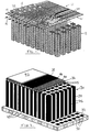
- Figure 1 shows a known 2D acoustic imaging array 10 comprising a backing layer 12, an interconnect layer 14, an array of acoustic elements 16, a common electrode 18 and matching elements 20 located in positions which correspond to the acoustic elements 16.
- the acoustic elements 16 comprise a piezoelectric ceramic material such as lead zirconate titanate. They are formed by dicing of a bulk piece of piezoelectric material. Electrical connections are formed on upper and lower faces of the elements to, respectively, the common electrode 18 and contact pads 22 on the interconnect layer 14.
- the interconnect layer 14 contains a number of metal tracks 24 each of which terminates in one of the contact pads 22. Although in Figure 1 the tracks are shown, conventionally they are contained within the body of the interconnect layer 14. This may be formed by any convenient route such as sintering and firing ceramic tape. Alternatively, it may comprise layers of a polyimide material.
- the backing layer 12 is a sound absorbent material and may be an epoxy resin.
- the purpose of the backing layer 12 is to absorb any sound waves which travel through the interconnect layer 14 to prevent sound being reflected back to the elements from underneath. It comprises an array of rods 26 which are formed by dicing of a bulk piece of epoxy resin. The rods 26 all stand on, and are integrally part of, a base or substrate (not shown).
- the backing layer 12 is formed as a rod-like structure in order to isolate acoustically elements 16 from each other to prevent cross coupling and thus degrade sensitivity.
- the backing layer 12 has a large number of air gaps.
- it is constructed such that one matching element 20, one element 16, one contact pad 22 and one rod 26 are all in register in a single stack. This configuration of providing separate stacks for each acoustic element 16 is necessary in order to avoid cross-coupling between adjacent elements 16.
- Providing isolated rods 26 overcomes the problem of cross coupling to some extent, but further problems are created by the rod-like structure having air gaps. If the array 10 is to be used underwater, water pressure can damage the rod-like structure.
- a 2D acoustic imaging array 30 according to the invention is shown in Figure 2. It comprises an interconnect layer 32 carrying a backing layer 34 onto which is located a piezoelectric layer 36. A common electrode 38 is present on an upper face 40 of the piezoelectric layer 36. A matching layer 42 is present on an upper face 44 of the common electrode 28.
- the piezoelectric layer 36 is in the form of a 1-3 composite. This is formed by dicing a sheet of piezoelectric material into elongate members 45 and then backfilling with a filler which forms a matrix supporting the piezoelectric elongate members.
- the piezoelectric material is a ceramic such as lead zirconate titanate (PZT).
- the matrix is a polymer such as epoxy resin. It provides rigidity to the piezoelectric material for ease of handling during manufacture and ruggedness in use. In comparison with the known array the array 30 is more pressure resistant which is useful in underwater applications where pressure is to be resisted.
- the matching layer 42 can be an integral layer rather than a plurality of matching elements.
- the backing layer 34 has also been formed by dicing of a bulk material and backfilling. In this case it results in an epoxy resin structure having tungsten loaded conductive paths 46 in a matrix of non-loaded insulator 48.
- the piezoelectric layer 36 is in contact with the backing layer 34. It is important that this contact establishes good electrical contact between the elongate members 45 and the conductive paths 46 and so contact elements (not shown) are located on the back of the piezoelectric layer 36. Since this layer is in bulk rather than as discrete elements in the known array 10, it means that contact elements of any desired shape can be printed on the back of the layer to connect to (and activate) any desired shape of elongate members 45 to define individual elements. This is not possible in the known array 10 since the elements are separated by air gaps and are thus discrete.
- the conductive paths 46 are electrically connected to the piezoelectric layer 36. If the contact elements were the same size and shape as the ends of the conductive paths 46, the ends as seen in Figure 2 would define the elongate members 45 which comprise an individual element. At another end the conductive paths 46 are electrically connected to contact pads 50 on the interconnect layer.
- electronics for controlling operation of the acoustic elements may be integrated directly on to the interconnect layer (either in it or underneath it) rather than being located remote from the array as in the known array 10. This gives improved performance as well as weight reduction since the track lengths between the piezoelectric layer and the electronics can be minimised.
- a number of acoustic elements are grouped into sub-arrays.
- Figure 3 shows such a sub-array 60 having a backing layer 62 supported on an interconnect layer 64. The figure does not show a piezoelectric layer although, of course, one would be present in a practical embodiment.
- Tracks 66 running through the interconnect layer connect conductive paths 68 in the backing layer to contacts 70 on a transmit/readout chip 72.
- the readout chip 72 also carries contacts for input of power and control and output of data.
- the readout chip 72 may be mounted by a flip-chip solder bonding technique onto the back of the interconnect layer 66. Outputs from the sub-array 60 are connected to the readout chip 72 by fanning down the outputs onto the chip 72.
- the chip 72 may have 10x10 contacts for a sub-array of 10x10 elements and may be a few millimetres square compared with several centimetres square for a 100x100 array. Signals from the sub-array 60 (which represent a small part of an image detected by the entire array) are multiplexed in a separate multiplexer chip with signals from other sub-arrays to group together outputs of the elements in the entire array, for example 10,000, into a more manageable 100 outputs from 100 chips.
- This arrangement showing the chips 72 bonded to the back of the interconnect layer 64 is shown in Figure 4.
- a second interconnect layer connects to a main multiplexer which multiplexes together the outputs from all of the chips 72.
- the main multiplexer is bonded to the interconnect layer 64. Power is supplied to the chip along line 74 and timing and data outputs are taken from lines 76. Data is supplied by lines 76 to a data processor which can generate images.
- Typical array dimensions are 1mm 2 elements arranged at a pitch of 1.75mm. The dimensions depend on the operating frequency and required resolution and these values would be suitable for operation at 3MHz. Operation in the frequency range 0.1 to 20MHz is envisaged. The thickness of the backing layer would be about 10mm. The invention would be suitable for fabricating an array of 100x100 although larger arrays are possible, especially when using a modular system having sub-arrays.
- This embodiment can be used to steer a transmitted beam of acoustic energy. This may be achieved by transmitting a sonic beam which is steered by phasing the array in during transmission. The transmitted beam would be pulsed. An image may then be formed from signals received by the array.
- the system may comprise external acoustic imaging lenses.
- the array, backing material and/or interconnect layer may be shaped to provide self-focussing.
- the invention is particularly suitable for imaging in liquid. It could have civil or other applications and could be used for imaging in unclear water such as in a diver's helmet in conjunction with a head-up display or in a submersible vehicle for guidance or imaging systems. Alternatively, it could be used in a medical imaging system or for non-destructive testing of structures such as solids. Essentially the system may be used in any application to detect differences in acoustic impedances.
Applications Claiming Priority (2)
| Application Number | Priority Date | Filing Date | Title |
|---|---|---|---|
| GBGB9525418.1A GB9525418D0 (en) | 1995-12-13 | 1995-12-13 | Acoustic imaging arrays |
| GB9525418 | 1995-12-13 |
Publications (3)
| Publication Number | Publication Date |
|---|---|
| EP0779108A2 true EP0779108A2 (fr) | 1997-06-18 |
| EP0779108A3 EP0779108A3 (fr) | 1997-10-29 |
| EP0779108B1 EP0779108B1 (fr) | 2000-02-09 |
Family
ID=10785319
Family Applications (1)
| Application Number | Title | Priority Date | Filing Date |
|---|---|---|---|
| EP19960308744 Expired - Lifetime EP0779108B1 (fr) | 1995-12-13 | 1996-12-03 | Réseaux pour l'imagerie acoustique |
Country Status (4)
| Country | Link |
|---|---|
| EP (1) | EP0779108B1 (fr) |
| AU (1) | AU724201B2 (fr) |
| DE (1) | DE69606609T2 (fr) |
| GB (1) | GB9525418D0 (fr) |
Cited By (6)
| Publication number | Priority date | Publication date | Assignee | Title |
|---|---|---|---|---|
| FR2756447A1 (fr) * | 1996-11-26 | 1998-05-29 | Thomson Csf | Sonde acoustique multielements comprenant une electrode de masse commune |
| US6467138B1 (en) | 2000-05-24 | 2002-10-22 | Vermon | Integrated connector backings for matrix array transducers, matrix array transducers employing such backings and methods of making the same |
| EP1677575A2 (fr) * | 2004-12-20 | 2006-07-05 | Samsung Electronics Co., Ltd. | Ecran à la reproduction sonore pour un procédé à reproduire et à convertir l'ultrason |
| US7230368B2 (en) | 2004-04-20 | 2007-06-12 | Visualsonics Inc. | Arrayed ultrasonic transducer |
| US9935254B2 (en) | 2008-09-18 | 2018-04-03 | Fujifilm Sonosite, Inc. | Methods for manufacturing ultrasound transducers and other components |
| US10596597B2 (en) | 2008-09-18 | 2020-03-24 | Fujifilm Sonosite, Inc. | Methods for manufacturing ultrasound transducers and other components |
Families Citing this family (2)
| Publication number | Priority date | Publication date | Assignee | Title |
|---|---|---|---|---|
| EP1952175B1 (fr) | 2005-11-02 | 2013-01-09 | Visualsonics, Inc. | Formateur de faisceaux digital pour un système ultrasonore à réseau de transducteurs |
| EP3309823B1 (fr) | 2008-09-18 | 2020-02-12 | FUJIFILM SonoSite, Inc. | Transducteurs à ultrasons |
Family Cites Families (4)
| Publication number | Priority date | Publication date | Assignee | Title |
|---|---|---|---|---|
| GB1530783A (en) * | 1976-01-30 | 1978-11-01 | Emi Ltd | Ultra-sonic pickup device |
| US4801835A (en) * | 1986-10-06 | 1989-01-31 | Hitachi Medical Corp. | Ultrasonic probe using piezoelectric composite material |
| US5267221A (en) * | 1992-02-13 | 1993-11-30 | Hewlett-Packard Company | Backing for acoustic transducer array |
| US5329498A (en) * | 1993-05-17 | 1994-07-12 | Hewlett-Packard Company | Signal conditioning and interconnection for an acoustic transducer |
-
1995
- 1995-12-13 GB GBGB9525418.1A patent/GB9525418D0/en active Pending
-
1996
- 1996-12-03 DE DE1996606609 patent/DE69606609T2/de not_active Expired - Fee Related
- 1996-12-03 EP EP19960308744 patent/EP0779108B1/fr not_active Expired - Lifetime
- 1996-12-11 AU AU74293/96A patent/AU724201B2/en not_active Ceased
Non-Patent Citations (1)
| Title |
|---|
| None |
Cited By (13)
| Publication number | Priority date | Publication date | Assignee | Title |
|---|---|---|---|---|
| FR2756447A1 (fr) * | 1996-11-26 | 1998-05-29 | Thomson Csf | Sonde acoustique multielements comprenant une electrode de masse commune |
| WO1998023392A1 (fr) * | 1996-11-26 | 1998-06-04 | Thomson-Csf | Sonde acoustique multielements comprenant une electrode de masse commune |
| US6341408B2 (en) | 1996-11-26 | 2002-01-29 | Thomson-Csf | Method of manufacturing a multiple-element acoustic probe comprising a common ground electrode |
| US6467138B1 (en) | 2000-05-24 | 2002-10-22 | Vermon | Integrated connector backings for matrix array transducers, matrix array transducers employing such backings and methods of making the same |
| US7830069B2 (en) | 2004-04-20 | 2010-11-09 | Sunnybrook Health Sciences Centre | Arrayed ultrasonic transducer |
| US7230368B2 (en) | 2004-04-20 | 2007-06-12 | Visualsonics Inc. | Arrayed ultrasonic transducer |
| EP1677575A3 (fr) * | 2004-12-20 | 2008-12-24 | Samsung Electronics Co., Ltd. | Ecran à la reproduction sonore pour un procédé à reproduire et à convertir l'ultrason |
| EP1677575A2 (fr) * | 2004-12-20 | 2006-07-05 | Samsung Electronics Co., Ltd. | Ecran à la reproduction sonore pour un procédé à reproduire et à convertir l'ultrason |
| US7912227B2 (en) | 2004-12-20 | 2011-03-22 | Samsung Electronics Co., Ltd. | Sound reproducing screen for an ultrasonic converting and reproducing method |
| US9935254B2 (en) | 2008-09-18 | 2018-04-03 | Fujifilm Sonosite, Inc. | Methods for manufacturing ultrasound transducers and other components |
| US10596597B2 (en) | 2008-09-18 | 2020-03-24 | Fujifilm Sonosite, Inc. | Methods for manufacturing ultrasound transducers and other components |
| US11094875B2 (en) | 2008-09-18 | 2021-08-17 | Fujifilm Sonosite, Inc. | Methods for manufacturing ultrasound transducers and other components |
| US11845108B2 (en) | 2008-09-18 | 2023-12-19 | Fujifilm Sonosite, Inc. | Methods for manufacturing ultrasound transducers and other components |
Also Published As
| Publication number | Publication date |
|---|---|
| DE69606609D1 (de) | 2000-03-16 |
| EP0779108A3 (fr) | 1997-10-29 |
| AU7429396A (en) | 1997-06-19 |
| GB9525418D0 (en) | 1996-07-17 |
| EP0779108B1 (fr) | 2000-02-09 |
| AU724201B2 (en) | 2000-09-14 |
| DE69606609T2 (de) | 2000-06-08 |
Similar Documents
| Publication | Publication Date | Title |
|---|---|---|
| US6236144B1 (en) | Acoustic imaging arrays | |
| US7952260B2 (en) | Ultrasound imaging system | |
| US5329496A (en) | Two-dimensional array ultrasonic transducers | |
| JP5591549B2 (ja) | 超音波トランスデューサ、超音波プローブ、超音波トランスデューサの製造方法 | |
| US7892176B2 (en) | Monitoring or imaging system with interconnect structure for large area sensor array | |
| US20220079559A1 (en) | Modular piezoelectric sensor array with co-integrated electronics and beamforming channels | |
| US6776762B2 (en) | Piezocomposite ultrasound array and integrated circuit assembly with improved thermal expansion and acoustical crosstalk characteristics | |
| JP5611645B2 (ja) | 超音波トランスデューサおよび超音波プローブ | |
| US6640634B2 (en) | Ultrasonic probe, method of manufacturing the same and ultrasonic diagnosis apparatus | |
| US5732706A (en) | Ultrasonic array with attenuating electrical interconnects | |
| EP0637469A2 (fr) | Elément transducteur à couches multiples | |
| US5311095A (en) | Ultrasonic transducer array | |
| JP3865928B2 (ja) | 結合バッキングブロック及び複合変換器アレー | |
| EP1436097B1 (fr) | Systeme pour fixer un element acoustique a un circuit integre | |
| US4831601A (en) | Apparatus for transmitting and receiving ultrasonic signals | |
| US4640291A (en) | Bi-plane phased array for ultrasound medical imaging | |
| US5920972A (en) | Interconnection method for a multilayer transducer array | |
| US20090303838A1 (en) | Acoustic Sensor and Method | |
| US9423382B2 (en) | Test head for testing a workpiece having an ultrasonic transducer configuration containing a plurality of ultrasonic transducers and process for producing such a test head | |
| AU724201B2 (en) | Acoustic imaging arrays | |
| JPH0723500A (ja) | 2次元アレイ超音波プローブ | |
| JP2005210245A (ja) | 超音波プローブ | |
| US7249513B1 (en) | Ultrasound probe | |
| US20210356437A1 (en) | Scanning apparatus | |
| EP3895812B1 (fr) | Transducteur piézoélectrique de forme incurvée et son procédé de fabrication |
Legal Events
| Date | Code | Title | Description |
|---|---|---|---|
| PUAI | Public reference made under article 153(3) epc to a published international application that has entered the european phase |
Free format text: ORIGINAL CODE: 0009012 |
|
| AK | Designated contracting states |
Kind code of ref document: A2 Designated state(s): DE FR GB |
|
| PUAL | Search report despatched |
Free format text: ORIGINAL CODE: 0009013 |
|
| AK | Designated contracting states |
Kind code of ref document: A3 Designated state(s): DE FR GB |
|
| 17P | Request for examination filed |
Effective date: 19980429 |
|
| 17Q | First examination report despatched |
Effective date: 19980928 |
|
| RAP1 | Party data changed (applicant data changed or rights of an application transferred) |
Owner name: MARCONI ELECTRONIC SYSTEMS LIMITED |
|
| GRAG | Despatch of communication of intention to grant |
Free format text: ORIGINAL CODE: EPIDOS AGRA |
|
| GRAG | Despatch of communication of intention to grant |
Free format text: ORIGINAL CODE: EPIDOS AGRA |
|
| GRAG | Despatch of communication of intention to grant |
Free format text: ORIGINAL CODE: EPIDOS AGRA |
|
| GRAH | Despatch of communication of intention to grant a patent |
Free format text: ORIGINAL CODE: EPIDOS IGRA |
|
| GRAH | Despatch of communication of intention to grant a patent |
Free format text: ORIGINAL CODE: EPIDOS IGRA |
|
| GRAA | (expected) grant |
Free format text: ORIGINAL CODE: 0009210 |
|
| AK | Designated contracting states |
Kind code of ref document: B1 Designated state(s): DE FR GB |
|
| REF | Corresponds to: |
Ref document number: 69606609 Country of ref document: DE Date of ref document: 20000316 |
|
| ET | Fr: translation filed | ||
| REG | Reference to a national code |
Ref country code: GB Ref legal event code: 732E |
|
| RAP2 | Party data changed (patent owner data changed or rights of a patent transferred) |
Owner name: MARCONI CASWELL LIMITED |
|
| PLBE | No opposition filed within time limit |
Free format text: ORIGINAL CODE: 0009261 |
|
| STAA | Information on the status of an ep patent application or granted ep patent |
Free format text: STATUS: NO OPPOSITION FILED WITHIN TIME LIMIT |
|
| 26N | No opposition filed | ||
| REG | Reference to a national code |
Ref country code: FR Ref legal event code: TP |
|
| REG | Reference to a national code |
Ref country code: GB Ref legal event code: IF02 |
|
| REG | Reference to a national code |
Ref country code: GB Ref legal event code: 732E |
|
| REG | Reference to a national code |
Ref country code: FR Ref legal event code: TP |
|
| PGFP | Annual fee paid to national office [announced via postgrant information from national office to epo] |
Ref country code: GB Payment date: 20031203 Year of fee payment: 8 |
|
| PGFP | Annual fee paid to national office [announced via postgrant information from national office to epo] |
Ref country code: FR Payment date: 20031210 Year of fee payment: 8 |
|
| PGFP | Annual fee paid to national office [announced via postgrant information from national office to epo] |
Ref country code: DE Payment date: 20031211 Year of fee payment: 8 |
|
| PG25 | Lapsed in a contracting state [announced via postgrant information from national office to epo] |
Ref country code: GB Free format text: LAPSE BECAUSE OF NON-PAYMENT OF DUE FEES Effective date: 20041203 |
|
| REG | Reference to a national code |
Ref country code: FR Ref legal event code: CD |
|
| PG25 | Lapsed in a contracting state [announced via postgrant information from national office to epo] |
Ref country code: DE Free format text: LAPSE BECAUSE OF NON-PAYMENT OF DUE FEES Effective date: 20050701 |
|
| GBPC | Gb: european patent ceased through non-payment of renewal fee |
Effective date: 20041203 |
|
| PG25 | Lapsed in a contracting state [announced via postgrant information from national office to epo] |
Ref country code: FR Free format text: LAPSE BECAUSE OF NON-PAYMENT OF DUE FEES Effective date: 20050831 |
|
| REG | Reference to a national code |
Ref country code: FR Ref legal event code: ST |