EP0777902B1 - Elektrisch löschbarer und programmierbarer festwertspeicher mit nichtuniformer dieelektrischer dicke - Google Patents
Elektrisch löschbarer und programmierbarer festwertspeicher mit nichtuniformer dieelektrischer dicke Download PDFInfo
- Publication number
- EP0777902B1 EP0777902B1 EP96919972A EP96919972A EP0777902B1 EP 0777902 B1 EP0777902 B1 EP 0777902B1 EP 96919972 A EP96919972 A EP 96919972A EP 96919972 A EP96919972 A EP 96919972A EP 0777902 B1 EP0777902 B1 EP 0777902B1
- Authority
- EP
- European Patent Office
- Prior art keywords
- trench
- layer
- sidewall
- gate
- eeprom
- Prior art date
- Legal status (The legal status is an assumption and is not a legal conclusion. Google has not performed a legal analysis and makes no representation as to the accuracy of the status listed.)
- Expired - Lifetime
Links
- 239000004065 semiconductor Substances 0.000 claims abstract description 17
- 230000007423 decrease Effects 0.000 claims 1
- 230000005684 electric field Effects 0.000 abstract description 3
- VYPSYNLAJGMNEJ-UHFFFAOYSA-N Silicium dioxide Chemical compound O=[Si]=O VYPSYNLAJGMNEJ-UHFFFAOYSA-N 0.000 description 10
- 229910021420 polycrystalline silicon Inorganic materials 0.000 description 7
- 229920005591 polysilicon Polymers 0.000 description 6
- 235000012239 silicon dioxide Nutrition 0.000 description 5
- 239000000377 silicon dioxide Substances 0.000 description 5
- 239000000758 substrate Substances 0.000 description 4
- 238000010276 construction Methods 0.000 description 3
- 230000006870 function Effects 0.000 description 2
- 239000011810 insulating material Substances 0.000 description 2
- 239000000463 material Substances 0.000 description 2
- 229910052581 Si3N4 Inorganic materials 0.000 description 1
- 230000002411 adverse Effects 0.000 description 1
- 230000000694 effects Effects 0.000 description 1
- BHEPBYXIRTUNPN-UHFFFAOYSA-N hydridophosphorus(.) (triplet) Chemical compound [PH] BHEPBYXIRTUNPN-UHFFFAOYSA-N 0.000 description 1
- 238000000034 method Methods 0.000 description 1
- HQVNEWCFYHHQES-UHFFFAOYSA-N silicon nitride Chemical compound N12[Si]34N5[Si]62N3[Si]51N64 HQVNEWCFYHHQES-UHFFFAOYSA-N 0.000 description 1
Images

Classifications
-
- G—PHYSICS
- G11—INFORMATION STORAGE
- G11C—STATIC STORES
- G11C16/00—Erasable programmable read-only memories
- G11C16/02—Erasable programmable read-only memories electrically programmable
-
- H—ELECTRICITY
- H10—SEMICONDUCTOR DEVICES; ELECTRIC SOLID-STATE DEVICES NOT OTHERWISE PROVIDED FOR
- H10D—INORGANIC ELECTRIC SEMICONDUCTOR DEVICES
- H10D30/00—Field-effect transistors [FET]
- H10D30/01—Manufacture or treatment
- H10D30/021—Manufacture or treatment of FETs having insulated gates [IGFET]
- H10D30/0411—Manufacture or treatment of FETs having insulated gates [IGFET] of FETs having floating gates
-
- H—ELECTRICITY
- H10—SEMICONDUCTOR DEVICES; ELECTRIC SOLID-STATE DEVICES NOT OTHERWISE PROVIDED FOR
- H10B—ELECTRONIC MEMORY DEVICES
- H10B69/00—Erasable-and-programmable ROM [EPROM] devices not provided for in groups H10B41/00 - H10B63/00, e.g. ultraviolet erasable-and-programmable ROM [UVEPROM] devices
-
- H—ELECTRICITY
- H10—SEMICONDUCTOR DEVICES; ELECTRIC SOLID-STATE DEVICES NOT OTHERWISE PROVIDED FOR
- H10D—INORGANIC ELECTRIC SEMICONDUCTOR DEVICES
- H10D30/00—Field-effect transistors [FET]
- H10D30/60—Insulated-gate field-effect transistors [IGFET]
- H10D30/68—Floating-gate IGFETs
- H10D30/6891—Floating-gate IGFETs characterised by the shapes, relative sizes or dispositions of the floating gate electrode
- H10D30/6894—Floating-gate IGFETs characterised by the shapes, relative sizes or dispositions of the floating gate electrode having one gate at least partly in a trench
Definitions
- This invention relates to a an electrically erasable and programmable read only memory (EEPROM) cell, comprising
- an EEPROM device structure has a floating gate and a control gate, both of which are typically fabricated out of polycrystalline silicon doped with an appropriate doping material to render the polycrystalline conductive.
- a typical doping material is phosphorous.
- the floating gate is separated from a substrate region by a gate dielectric layer of insulating material such as silicon dioxide, while the substrate region includes source and drain regions with a channel region therebetween.
- the floating gate and the control gate are separated by an intergate dielectric, typically silicon dioxide.
- the basic principle upon which the EEPROM device operates is as follows: the charge is stored on the floating gate in a capacitive manner and can be subsequently electrically erased as described in U.S. Patent No. 5,146,426.
- trench-based EEPROM device structures such as the one described in Japanese Patent No. 3-280580, which shows a memory cell consisting of two transistors in series.
- One side of the trench is a stacked-gate MOSFET.
- the other side of the trench is a single gate MOSFET.
- the gate structures are separated from each other at the bottom of the trench.
- Japanese Patent No. 1-81368 shows an EEPROM device where the channel region is on the top surface of the substrate and only the tunnel oxide and first polysilicon layer extending into the trench.
- the inter-poly layer and second polysilicon layer are disposed outside the trench.
- U.S. Patent No. 4,990,979 shows a trench-based EEPROM device wherein two memory cells share a single trench.
- the channel region is on the top surface of the substrate and the gate oxide and tunnel oxide layers are separately formed.
- a compact EEPROM device such as the one described in U.S. Patent No. 5,146,426, includes an insulated control gate and an insulated floating gate formed in a trench within a semiconductor body.
- a surface-adjoining drain region is provided alongside an upper portion of a sidewall of the trench, while a source region is provided alongside the lower portion of the sidewall of the trench, with a channel region extending along the sidewall of the trench between the source and drain regions.
- the device is programmed through the trench sidewall portion which is adjacent the channel region, and is erased through a corner region in the bottom of the trench by causing a localized high electric field density in the comer region during the erase operation.
- Another trench-based EEPROM as disclosed in US Patent 5,386,132 comprises a floating gate extending over the top of the drain and separated from the drain by a dielectric layer which is thinner than the gate dielectric on the side walls of the trench.
- An EEPROM device in accordance with the invention is characterized in that the portion of said gate dielectric covering a first sidewall portion has a thickness different from the thickness of said gate dielectric covering other sidewall portions.
- the thickness of the dielectric is made non-uniform along at least one of the sidewalls. Therefore, the potential of the first polysilicon layer can be more effectively raised through the applied voltage of the second polysilicon layer than in a device having a uniformly thin dielectric layer on all sidewalls.
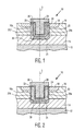
- FIGS. 1, 2 and 3 show a single transistor trench based electrically erasable and programmable read only memory (EEPROM) cell 10 in accordance with a first embodiment of the invention.
- Cell 10 is formed in a semiconductor body having a first semiconductor layer 12 of a first conductivity type (in this example n-type) and a doping level of about 10 19 at/cm 3 or higher.
- Semiconductor layer 12 can also be of a p-type having a doping level of 10 18 at/cm 3 or below.
- Cell 10 also includes a second semiconductor layer 14 of a first conductivity type (in this example n-type) on the first layer and having a lower doping level of about 10 18 at/cm 3 and a thickness of about 0.5 ⁇ .
- the first and second layers form the source region of the EEPROM cell.
- a third semiconductor layer 16 having a second conductivity type (here p-type) is provided on second layer 14 and extends to the surface of cell 10. The thickness of this layer is about 0.6 - 1.0 ⁇ and its doping level is about 5 X 10 17 at/cm 3 .
- a fourth surface-adjoining, highly-doped semiconductor layer 18 of a first conductivity type (in this example, n-type) is provided locally in the third layer and forms a drain region of cell 10. Fourth layer 18 has a doping level of about 10 20 at/cm 3 and a thickness of about 0.1 - 0.4 ⁇ .
- a trench 20 having a floor 21 and sidewall portions 20a, 20b, 20c and 20d extends through third layer 16 and fourth layer 18 and partly into second layer 14.
- trench 20 has a substantially square configuration, however the shape of trench 20 is not limited to that shown in FIGS. 1 and 2 and can have a rectangular, circular or other shape.
- a channel region 16a is located in a portion of third layer 16 adjacent sidewall portions 20a, 20b, 20c and 20d and extending in a substantially vertical direction from the source region to the drain region of the device.
- Sidewall portions 20a, 20b, 20c and 20d and floor 21 are covered with a gate dielectric 22 formed of an insulating material such as silicon dioxide.
- FIGS. 1 and 2 show an EEPROM device in accordance with a first embodiment of the invention.
- Reference numerals mentioned above with respect to FIG. 1 refer to the same elements in the following figures.
- the thickness of gate dielectric 22 of sidewall portions 20a and 20c is about 100A while the thickness of gate dielectric 22 on sidewall portions 20b and 20d is substantially thicker, for example, about 1000A.
- a floating gate 24 is formed of polysilicon and is provided on gate dielectric 22 and extends to adjacent sidewall portions 20a, 20b, 20c and 20d and floor 21.
- the interior portions of floating gate 24 are covered by an intergate dielectric 26 formed of a layer of silicon dioxide or silicon dioxide and silicon nitride having a thickness of about 200 Angstroms.
- control gate 28 formed of polysilicon on intergate dielectric 28 and extending within trench 20 to about the same depth as third layer 16, with control gate 28 being separated from channel region 16a by floating gate 24, gate dielectric 22 and intergate dielectric 26.
- FIG. 4 shows an EEPROM cell in accordance with a second embodiment of the present invention.
- This embodiment differs from the first in that the thickness of dielectric layer 22 over sidewalls 20b and 20d varies across the length of each sidewall from about 1000A to about 100A.
- the thickness of dielectric layer 22 over sidewalls 20a and 20c is the same as shown in FIG. 2 and discussed above with respect to the first embodiment.
- dielectric layer 22 is kept relatively thin near the bottom of the trench in order to provide superior electrical erase performance.
Landscapes
- Non-Volatile Memory (AREA)
- Semiconductor Memories (AREA)
- Read Only Memory (AREA)
Claims (4)
- Elektrisch löschbare und programmierbare Festwertspeicher-(EEPROM)-Zelle (10) mitdadurch gekennzeichnet, dass der Teil des Gatedielektrikums, mit welchem eine erste Seitenwand (20b, 20d) versehen ist, eine andere Stärke als diese des Gatedielektrikums, mit welchem die anderen Seitenwände (20a, 20c) versehen sind, aufweist.einer ersten Halbleiterschicht (12) eines ersten Leitfähigkeitstyps;einer zweiten Halbleiterschicht (14) des ersten Leitfähigkeitstyps, welche auf der ersten Schicht aufgebracht ist und ein niedrigeres Dotierungsniveau als dieses der ersten Schicht aufweist, wobei die erste und die zweite Schicht zusammen einen Sourcebereich der EEPROM-Zelle bilden;einer dritten Halbleiterschicht (16) eines zweiten, entgegengesetzten Leitfähigkeitstyps, welche auf der zweiten Schicht angeordnet ist und sich bis zu einer Oberfläche der EEPROM-Zelle erstreckt;einer vierten, oberflächenangrenzenden Halbleiterschicht (18) des ersten Leitfähigkeitstyps, welche in der dritten Schicht lokal vorgesehen ist und einen Drainbereich der EEPROM-Zelle bildet;einem Graben (20), welcher sich durch die dritte und vierte Schicht und zum Teil in die zweite Schicht erstreckt, wobei der Graben einen Boden (21) und Seitenwände (20a, 20b, 20c, 20d) aufweist;einem Kanalbereich (16a), welcher in einem Teil der dritten Schicht in Angrenzung an eine Seitenwand des Grabens angeordnet ist und sich von der zweiten bis zur vierten Zone erstreckt;einem Gatedielektrikum (22), mit welchem die Seitenwände und der Boden des Grabens versehen sind;einem schwebenden Gate (24), welches auf dem Gatedielektrikum vorgesehen ist und sich in Angrenzung an die Seitenwände und den Boden des Grabens erstreckt,einem Intergatedielektrikum (26), mit welchem zumindest eine Innenseitenwand und der Boden des schwebenden Gates versehen sind; sowieeinem Steuergate (28), welches auf dem Intergatedielektrikum vorgesehen und von dem Kanalbereich durch das schwebende Gate getrennt ist,
- EEPROM-Zelle nach Anspruch 1, dadurch gekennzeichnet, dass der Graben eine quadratische Form aufweist.
- EEPROM-Zelle nach Anspruch 1, dadurch gekennzeichnet, dass der Graben eine kreisförmige Form aufweist.
- EEPROM-Zelle nach Anspruch 1, dadurch gekennzeichnet, dass das Gatedielektrikum, mit welchem die erste Seitenwand (20b, 20d) versehen ist, eine Dicke aufweist, welche entlang der ersten Seitenwand zum Boden hin abnimmt (Fig. 4).
Applications Claiming Priority (3)
| Application Number | Priority Date | Filing Date | Title |
|---|---|---|---|
| US496104 | 1995-06-28 | ||
| US08/496,104 US5606521A (en) | 1995-06-28 | 1995-06-28 | Electrically erasable and programmable read only memory with non-uniform dielectric thickness |
| PCT/IB1996/000578 WO1997001847A2 (en) | 1995-06-28 | 1996-06-14 | Electrically erasable and programmable read only memory with non-uniform dielectric thickness |
Publications (3)
| Publication Number | Publication Date |
|---|---|
| EP0777902A2 EP0777902A2 (de) | 1997-06-11 |
| EP0777902A3 EP0777902A3 (de) | 1997-07-09 |
| EP0777902B1 true EP0777902B1 (de) | 2001-10-17 |
Family
ID=23971250
Family Applications (1)
| Application Number | Title | Priority Date | Filing Date |
|---|---|---|---|
| EP96919972A Expired - Lifetime EP0777902B1 (de) | 1995-06-28 | 1996-06-14 | Elektrisch löschbarer und programmierbarer festwertspeicher mit nichtuniformer dieelektrischer dicke |
Country Status (6)
| Country | Link |
|---|---|
| US (1) | US5606521A (de) |
| EP (1) | EP0777902B1 (de) |
| JP (1) | JPH10505464A (de) |
| KR (1) | KR970705820A (de) |
| DE (1) | DE69615995T2 (de) |
| WO (1) | WO1997001847A2 (de) |
Families Citing this family (27)
| Publication number | Priority date | Publication date | Assignee | Title |
|---|---|---|---|---|
| US7071060B1 (en) * | 1996-02-28 | 2006-07-04 | Sandisk Corporation | EEPROM with split gate source side infection with sidewall spacers |
| US6222762B1 (en) | 1992-01-14 | 2001-04-24 | Sandisk Corporation | Multi-state memory |
| US5712180A (en) * | 1992-01-14 | 1998-01-27 | Sundisk Corporation | EEPROM with split gate source side injection |
| US5313421A (en) * | 1992-01-14 | 1994-05-17 | Sundisk Corporation | EEPROM with split gate source side injection |
| JP3403877B2 (ja) * | 1995-10-25 | 2003-05-06 | 三菱電機株式会社 | 半導体記憶装置とその製造方法 |
| FR2767219B1 (fr) * | 1997-08-08 | 1999-09-17 | Commissariat Energie Atomique | Dispositif memoire non volatile programmable et effacable electriquement compatible avec un procede de fabrication cmos/soi |
| US5972753A (en) * | 1997-12-04 | 1999-10-26 | Taiwan Semiconductor Manufacturing Company, Ltd. | Method of self-align cell edge implant to reduce leakage current and improve program speed in split-gate flash |
| US6002151A (en) * | 1997-12-18 | 1999-12-14 | Advanced Micro Devices, Inc. | Non-volatile trench semiconductor device |
| US6274900B1 (en) | 1998-01-05 | 2001-08-14 | Texas Instruments Incorporated | Semiconductor device architectures including UV transmissive nitride layers |
| US5923063A (en) * | 1998-02-19 | 1999-07-13 | Advanced Micro Devices, Inc. | Double density V nonvolatile memory cell |
| US6420975B1 (en) | 1999-08-25 | 2002-07-16 | Donnelly Corporation | Interior rearview mirror sound processing system |
| US6093616A (en) * | 1998-05-11 | 2000-07-25 | Taiwan Semiconductor Manufacturing Company | Method of manufacture of stacked gate MOS structure for multiple voltage power supply applications |
| EP0969507B1 (de) | 1998-06-30 | 2006-11-15 | STMicroelectronics S.r.l. | Verfahren zur Herstellung einer EEPROM-Speicherzelle |
| JP2000208647A (ja) * | 1999-01-12 | 2000-07-28 | Internatl Business Mach Corp <Ibm> | Eepromメモリセル及びその製造方法 |
| US6151248A (en) | 1999-06-30 | 2000-11-21 | Sandisk Corporation | Dual floating gate EEPROM cell array with steering gates shared by adjacent cells |
| US6091633A (en) * | 1999-08-09 | 2000-07-18 | Sandisk Corporation | Memory array architecture utilizing global bit lines shared by multiple cells |
| US6087695A (en) * | 1999-08-20 | 2000-07-11 | Worldwide Semiconductor Mfg | Source side injection flash EEPROM memory cell with dielectric pillar and operation |
| US6750122B1 (en) * | 1999-09-29 | 2004-06-15 | Infineon Technologies Ag | Semiconductor device formed with an oxygen implant step |
| US6249022B1 (en) * | 1999-10-22 | 2001-06-19 | United Microelectronics Corp. | Trench flash memory with nitride spacers for electron trapping |
| US6512263B1 (en) | 2000-09-22 | 2003-01-28 | Sandisk Corporation | Non-volatile memory cell array having discontinuous source and drain diffusions contacted by continuous bit line conductors and methods of forming |
| US6936887B2 (en) * | 2001-05-18 | 2005-08-30 | Sandisk Corporation | Non-volatile memory cells utilizing substrate trenches |
| US6894343B2 (en) * | 2001-05-18 | 2005-05-17 | Sandisk Corporation | Floating gate memory cells utilizing substrate trenches to scale down their size |
| TW573344B (en) * | 2002-05-24 | 2004-01-21 | Nanya Technology Corp | Separated gate flash memory and its manufacturing method |
| TWI283912B (en) * | 2002-10-21 | 2007-07-11 | Nanya Technology Corp | A trench type stacked gate flash memory and the method to fabricate the same |
| KR100526478B1 (ko) * | 2003-12-31 | 2005-11-08 | 동부아남반도체 주식회사 | 반도체 소자 및 그 제조방법 |
| US7312490B2 (en) * | 2005-03-31 | 2007-12-25 | Intel Corporation | Vertical memory device and method |
| US10103226B2 (en) * | 2012-04-30 | 2018-10-16 | International Business Machines Corporation | Method of fabricating tunnel transistors with abrupt junctions |
Family Cites Families (7)
| Publication number | Priority date | Publication date | Assignee | Title |
|---|---|---|---|---|
| US5017977A (en) * | 1985-03-26 | 1991-05-21 | Texas Instruments Incorporated | Dual EPROM cells on trench walls with virtual ground buried bit lines |
| JPS6481368A (en) * | 1987-09-24 | 1989-03-27 | Oki Electric Ind Co Ltd | Nonvolatile semiconductor device |
| DE3816358A1 (de) * | 1988-05-13 | 1989-11-23 | Eurosil Electronic Gmbh | Nichtfluechtige speicherzelle und verfahren zur herstellung |
| JPH03280580A (ja) * | 1990-03-29 | 1991-12-11 | Matsushita Electron Corp | 半導体記憶装置およびその製造方法 |
| US5071782A (en) * | 1990-06-28 | 1991-12-10 | Texas Instruments Incorporated | Vertical memory cell array and method of fabrication |
| US5146426A (en) * | 1990-11-08 | 1992-09-08 | North American Philips Corp. | Electrically erasable and programmable read only memory with trench structure |
| US5386132A (en) * | 1992-11-02 | 1995-01-31 | Wong; Chun C. D. | Multimedia storage system with highly compact memory device |
-
1995
- 1995-06-28 US US08/496,104 patent/US5606521A/en not_active Expired - Fee Related
-
1996
- 1996-06-14 KR KR1019970701228A patent/KR970705820A/ko not_active Abandoned
- 1996-06-14 JP JP9504276A patent/JPH10505464A/ja active Pending
- 1996-06-14 DE DE69615995T patent/DE69615995T2/de not_active Expired - Fee Related
- 1996-06-14 WO PCT/IB1996/000578 patent/WO1997001847A2/en not_active Ceased
- 1996-06-14 EP EP96919972A patent/EP0777902B1/de not_active Expired - Lifetime
Also Published As
| Publication number | Publication date |
|---|---|
| DE69615995D1 (de) | 2001-11-22 |
| DE69615995T2 (de) | 2002-04-25 |
| US5606521A (en) | 1997-02-25 |
| WO1997001847A3 (en) | 1997-02-20 |
| EP0777902A3 (de) | 1997-07-09 |
| EP0777902A2 (de) | 1997-06-11 |
| KR970705820A (ko) | 1997-10-09 |
| JPH10505464A (ja) | 1998-05-26 |
| WO1997001847A2 (en) | 1997-01-16 |
Similar Documents
| Publication | Publication Date | Title |
|---|---|---|
| EP0777902B1 (de) | Elektrisch löschbarer und programmierbarer festwertspeicher mit nichtuniformer dieelektrischer dicke | |
| US5146426A (en) | Electrically erasable and programmable read only memory with trench structure | |
| KR940006094B1 (ko) | 불휘발성 반도체 기억장치 및 그 제조방법 | |
| US5411905A (en) | Method of making trench EEPROM structure on SOI with dual channels | |
| US7417278B2 (en) | Method to increase coupling ratio of source to floating gate in split-gate flash | |
| US5108939A (en) | Method of making a non-volatile memory cell utilizing polycrystalline silicon spacer tunnel region | |
| US5614747A (en) | Method for manufacturing a flash EEPROM cell | |
| US6136653A (en) | Method and device for producing undercut gate for flash memory | |
| US5923063A (en) | Double density V nonvolatile memory cell | |
| US5574685A (en) | Self-aligned buried channel/junction stacked gate flash memory cell | |
| EP0812019A1 (de) | Nichtflüchtige Speicherzelle mit einzigem Gate und Verfahren zur Benutzung | |
| EP1091392B1 (de) | Herstellungsverfahren für eine profilierte Freischwebegatezelle | |
| US5057886A (en) | Non-volatile memory with improved coupling between gates | |
| US6248631B1 (en) | Method for forming a v-shaped floating gate | |
| KR20000048526A (ko) | 자기 정렬 비휘발성 메모리 셀 | |
| US7408230B2 (en) | EEPROM device having first and second doped regions that increase an effective channel length | |
| US5468981A (en) | Self-aligned buried channel/junction stacked gate flash memory cell | |
| US6362504B1 (en) | Contoured nonvolatile memory cell | |
| JPH05291586A (ja) | 不揮発性半導体記憶装置及びその製造方法 | |
| US7256449B2 (en) | EEPROM device for increasing a coupling ratio and fabrication method thereof | |
| US6424003B2 (en) | EEPROM cell with self-aligned tunneling window | |
| US6320219B1 (en) | Memory cell for EEPROM devices and corresponding fabricating process | |
| US6348710B1 (en) | Non-volatile semiconductor memory device | |
| JP2536686B2 (ja) | 不揮発性メモリ | |
| JP4928019B2 (ja) | フローテイングゲート・メモリセル用のv字形状フローテイングゲートを形成する方法 |
Legal Events
| Date | Code | Title | Description |
|---|---|---|---|
| PUAI | Public reference made under article 153(3) epc to a published international application that has entered the european phase |
Free format text: ORIGINAL CODE: 0009012 |
|
| PUAK | Availability of information related to the publication of the international search report |
Free format text: ORIGINAL CODE: 0009015 |
|
| AK | Designated contracting states |
Kind code of ref document: A2 Designated state(s): DE FR GB NL |
|
| AK | Designated contracting states |
Kind code of ref document: A3 Designated state(s): DE FR GB NL |
|
| RHK1 | Main classification (correction) |
Ipc: G11C 16/02 |
|
| 17P | Request for examination filed |
Effective date: 19970716 |
|
| 17Q | First examination report despatched |
Effective date: 19991110 |
|
| GRAG | Despatch of communication of intention to grant |
Free format text: ORIGINAL CODE: EPIDOS AGRA |
|
| GRAG | Despatch of communication of intention to grant |
Free format text: ORIGINAL CODE: EPIDOS AGRA |
|
| GRAH | Despatch of communication of intention to grant a patent |
Free format text: ORIGINAL CODE: EPIDOS IGRA |
|
| GRAH | Despatch of communication of intention to grant a patent |
Free format text: ORIGINAL CODE: EPIDOS IGRA |
|
| GRAA | (expected) grant |
Free format text: ORIGINAL CODE: 0009210 |
|
| AK | Designated contracting states |
Kind code of ref document: B1 Designated state(s): DE FR GB NL |
|
| PG25 | Lapsed in a contracting state [announced via postgrant information from national office to epo] |
Ref country code: NL Free format text: LAPSE BECAUSE OF FAILURE TO SUBMIT A TRANSLATION OF THE DESCRIPTION OR TO PAY THE FEE WITHIN THE PRESCRIBED TIME-LIMIT Effective date: 20011017 |
|
| REF | Corresponds to: |
Ref document number: 69615995 Country of ref document: DE Date of ref document: 20011122 |
|
| REG | Reference to a national code |
Ref country code: GB Ref legal event code: IF02 |
|
| ET | Fr: translation filed | ||
| NLV1 | Nl: lapsed or annulled due to failure to fulfill the requirements of art. 29p and 29m of the patents act | ||
| PGFP | Annual fee paid to national office [announced via postgrant information from national office to epo] |
Ref country code: FR Payment date: 20020625 Year of fee payment: 7 |
|
| PGFP | Annual fee paid to national office [announced via postgrant information from national office to epo] |
Ref country code: GB Payment date: 20020628 Year of fee payment: 7 |
|
| PGFP | Annual fee paid to national office [announced via postgrant information from national office to epo] |
Ref country code: DE Payment date: 20020821 Year of fee payment: 7 |
|
| PLBE | No opposition filed within time limit |
Free format text: ORIGINAL CODE: 0009261 |
|
| STAA | Information on the status of an ep patent application or granted ep patent |
Free format text: STATUS: NO OPPOSITION FILED WITHIN TIME LIMIT |
|
| 26N | No opposition filed | ||
| REG | Reference to a national code |
Ref country code: FR Ref legal event code: D6 |
|
| REG | Reference to a national code |
Ref country code: GB Ref legal event code: 746 Effective date: 20021111 |
|
| PG25 | Lapsed in a contracting state [announced via postgrant information from national office to epo] |
Ref country code: GB Free format text: LAPSE BECAUSE OF NON-PAYMENT OF DUE FEES Effective date: 20030614 |
|
| PG25 | Lapsed in a contracting state [announced via postgrant information from national office to epo] |
Ref country code: DE Free format text: LAPSE BECAUSE OF NON-PAYMENT OF DUE FEES Effective date: 20040101 |
|
| GBPC | Gb: european patent ceased through non-payment of renewal fee |
Effective date: 20030614 |
|
| PG25 | Lapsed in a contracting state [announced via postgrant information from national office to epo] |
Ref country code: FR Free format text: LAPSE BECAUSE OF NON-PAYMENT OF DUE FEES Effective date: 20040227 |
|
| REG | Reference to a national code |
Ref country code: FR Ref legal event code: ST |