EP0777321B1 - Amplification de tension à large plage de variation et convertisseur analogique/numérique comportant un tel amplificateur - Google Patents
Amplification de tension à large plage de variation et convertisseur analogique/numérique comportant un tel amplificateur Download PDFInfo
- Publication number
- EP0777321B1 EP0777321B1 EP96203266A EP96203266A EP0777321B1 EP 0777321 B1 EP0777321 B1 EP 0777321B1 EP 96203266 A EP96203266 A EP 96203266A EP 96203266 A EP96203266 A EP 96203266A EP 0777321 B1 EP0777321 B1 EP 0777321B1
- Authority
- EP
- European Patent Office
- Prior art keywords
- transistor
- voltage
- amplifier
- collector
- intermediate node
- Prior art date
- Legal status (The legal status is an assumption and is not a legal conclusion. Google has not performed a legal analysis and makes no representation as to the accuracy of the status listed.)
- Expired - Lifetime
Links
- 230000003321 amplification Effects 0.000 title 1
- 238000003199 nucleic acid amplification method Methods 0.000 title 1
- 235000021183 entrée Nutrition 0.000 description 18
- 230000006870 function Effects 0.000 description 13
- 230000007423 decrease Effects 0.000 description 3
- 238000010586 diagram Methods 0.000 description 3
- 230000000694 effects Effects 0.000 description 3
- 230000003247 decreasing effect Effects 0.000 description 2
- 230000000750 progressive effect Effects 0.000 description 2
- 230000006399 behavior Effects 0.000 description 1
- 238000006243 chemical reaction Methods 0.000 description 1
- 239000004020 conductor Substances 0.000 description 1
- 230000007425 progressive decline Effects 0.000 description 1
Images


Classifications
-
- H—ELECTRICITY
- H03—ELECTRONIC CIRCUITRY
- H03F—AMPLIFIERS
- H03F1/00—Details of amplifiers with only discharge tubes, only semiconductor devices or only unspecified devices as amplifying elements
- H03F1/32—Modifications of amplifiers to reduce non-linear distortion
- H03F1/3211—Modifications of amplifiers to reduce non-linear distortion in differential amplifiers
Definitions
- the present invention relates to a voltage amplifier, intended to receive an input voltage and to supply a voltage of output, comprising an amplifier stage including a first and a second transistors mounted in differential pair, the base of the first transistor being intended to receive the input voltage, the base of the second transistor being intended to receive a voltage opposite to said input voltage, the collector of the first transistor being connected to a positive supply terminal by a first branch comprising a resistive load, the collector of the second transistor, intended for supply the output voltage, being connected to the positive terminal supply by a second branch comprising a resistive load.
- the object of the present invention is to remedy these disadvantages, by proposing a voltage amplifier whose linearity of the transfer characteristic is improved near the limits of the range of variation of the output voltage, while presenting a limited number of transistor stages between the two potentials circuit supply.
- an amplifier of voltage of the type defined in the introductory paragraph is characterized by that the second branch is formed of at least two resistive elements connected in series, thus presenting at least one first node therebetween intermediate between the positive supply terminal and the collector of the second transistor, in that it is provided with a third branch comprising a resistive element placed in series with a current source, which third branch is disposed between the positive terminal supply and a negative supply terminal and present between the resistive element and the current source a second node intermediate, and in that it is provided with means for carrying out a comparison between the potential of the second intermediate node and that the collector of the first transistor on the one hand, and between the potential of the second intermediate node and that of the collector of the second transistor on the other hand, and to add to the current output in a portion of the resistive load of the second branch, a first current which gradually vanishes when the collector potential of the first transistor becomes lower than that of the second node intermediate and a second current which gradually vanishes when the potential of the collector of the second branch
- a particularly advantageous embodiment of the invention presents a voltage amplifier characterized in that the means of comparison between the potential of the second node intermediate and that of the collector of the first transistor on the one hand, and between the potential of the second intermediate node and that of the collector of the second transistor on the other hand respectively comprise a third and fourth transistors mounted in differential pair on the one hand, a fifth and a sixth transistors mounted in pair differential on the other hand, the base of the third transistor being connected to the collector of the first transistor, that of the fourth transistor to second intermediate node, the base of the fifth transistor being connected to the collector of the second transistor, that of the sixth transistor at the second intermediate node, the collectors of the third and sixth transistors being connected to the first intermediate node.
- the amplifier thus has a limited number of transistor stages between the two supply terminals of the circuit, the sum of the voltage drops across the various transistors therefore being also limited, which makes the amplifier particularly suitable for "bass” applications tensions ".
- a variant of the invention makes it possible to adjust the thresholds of comparison, without significantly changing the gain of the amplifier, in order to limit the effects of the correction made at the output voltage at the only variation ranges where the latter evolves in a non-linear way.
- Such a voltage amplifier is characterized in that the resistive element separating the positive supply terminal from the first intermediate node and the resistive element included in the third branch have a similar value, and in that the current supplied by the current source included in the third branch has a similar value of the maximum value of the current flowing in the second transistor.
- a voltage amplifier according to another variant of the invention is characterized in that the resistive element separating the first intermediate node of the positive supply terminal has a value lower than that of the resistive element separating the first node intermediate of the collector of the second transistor.
- An amplifier according to the invention has, in addition to the advantage to have an improved linearity transfer characteristic on a wider range of variation of the input voltage, that of provide a single, non-differential output, which makes it particularly suitable for conversion type applications analog / digital, where the amplifier output voltage is compared to a range of reference voltages, also of a non- differential.
- FIG. 1 schematically describes an amplifier of AD voltage according to the invention.
- Two transistors Q1 and Q2 are mounted in differential pair: the emitter of transistor Q1 is connected to one of the terminals of a resistor, the emitter of transistor Q2 being connected to the other terminal of the same resistance.
- Each of the two transmitters is linked to one terminal of a current source I1, the other terminal of said source of current being connected to a negative supply terminal, called GND.
- the base of transistor Q1 receives the input voltage from the amplifier voltage, called Vin, the base of transistor Q2 receiving the opposite of said input voltage, ie -Vin.
- the collector of the first transistor Q1 is connected to a positive supply terminal, called VCC, by a first branch comprising a resistive load, the collector of the second transistor Q2, supplying the output voltage called Vout, being connected to the positive VCC supply terminal by a second branch with a resistive load.
- the first branch is formed a resistive element R1.
- the second branch is made up of at least two resistive elements, called R21 and R22, connected in series and having between them at least a first intermediate node, called NI, between the positive supply terminal VCC and the collector of the second transistor Q2.
- the AD voltage amplifier has a third branch comprising a resistive element R3 placed in series with a source current I3, which third branch is arranged between the terminal positive supply VCC and the negative supply terminal GND and between the resistive element R3 and the current source I3 a second intermediate node.
- the voltage amplifier is also provided with means 10 and 11 for carrying out a comparison between the potential of the second intermediate node, called Vref, and that of the collector of first transistor Q1 on the one hand, and between the potential of the second node intermediate Vref and that of the collector of the second transistor Q2 on the other hand.
- FIG. 2 schematically describes an amplifier of voltage AD according to an advantageous embodiment of the invention.
- the amplifier stage structures and branches with resistive loads are identical to those described in Figure 1.
- a embodiment of the means 10 and 11 is further exposed: include a third transistor Q3 and a fourth respectively transistor Q4, mounted in differential pair, and a fifth transistor Q5 and a sixth transistor Q6, connected in differential pair.
- the base of the third transistor Q3 is connected to the collector of the first transistor Q1, that of the fourth transistor Q4 at the second intermediate node
- the base of the fifth transistor Q5 is connected to the collector of the second transistor Q2, that of the sixth transistor Q6 at the second node intermediate.
- the collectors of the third and sixth transistors Q3 and Q6 are connected to the first intermediate node NI, and those of the fourth and fifth transistors Q4 and Q5 to the positive supply terminal VCC.
- the resistive element R21 and the resistive element R3 included in the third branch have a value neighbor, and the current delivered by the current source I3 has a value close to the maximum value of the current flowing in the second transistor Q2, which is of the order of 2.I1.
- the element resistive R21 has a value lower than that of the resistive element R22. We choose R21 lower than R22 / 10, so that the voltage drop at terminals of R21 only causes a corrective effect on the output voltage Vout.
- the value of the resistive load of the first branch R1 is equal to the sum of the values of the resistive elements R21 and R22 composing the resistive load of the second branch.
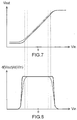
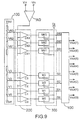
- FIGS 3 to 7 describe the evolution of various signals internal to the AD amplifier depending on the input voltage of this one, in order to facilitate the comprehension of its operation.
- Figure 3 describes the evolution of potentials VC1 and VC2, in function of the input voltage Vin of the amplifier AD.
- Figures 4 and 5 describe the evolution of the first and second currents, respectively I0 and I0 ', added in a portion of the load resistive, in this case R21, as a function of the input voltage Vin of the AD amplifier.
- Figure 6 describes the evolution of the total current in said portion of the resistive load R21 as a function of the voltage input of the AD amplifier.
- the IR210 curve represents the current which would circulate in the second branch if means 10 and 11 did not exist, i.e. in the case of the differential pair classic.
- the transistor Q1 When Vin is negative and large in absolute value, the transistor Q1 is not very conductive while transistor Q2 is very driver. The current in the first branch is therefore very weak, while the current in the second branch is important. The fall of voltage in the resistive element R1 is negligible, while the drops of voltage in the resistive elements R21 and R22 are significant.
- VC1 is then clearly greater than Vref.
- the transistor Q4 is therefore not very conductive while transistor Q3 is very conductor and passes a current I0 through the resistor R21. Vref being clearly superior to VC2, the transistor Q5 is not very conductive while the transistor Q6 is very conductive and passes a current Additional I0 'through resistor R21.
- transistor Q1 When Vin increases, while remaining negative, the first non-linear operating area of the conventional amplifier stage is reached: transistor Q1 conducts more, while transistor Q2 conducts less, the current flowing in the first branch increases while the current flowing in the second branch decreases.
- the potentials VC1 and Vref get closer, increasing the conduction of Q4 and decreasing the conduction of Q3, causing the progressive cancellation of the current I0 passing through resistor R21.
- the transistor Q5 remains not very conductive then that transistor Q6 remains very conductive, and maintains circulation of the current I0 'through the resistor R21.
Landscapes
- Physics & Mathematics (AREA)
- Nonlinear Science (AREA)
- Engineering & Computer Science (AREA)
- Power Engineering (AREA)
- Amplifiers (AREA)
- Analogue/Digital Conversion (AREA)
Applications Claiming Priority (2)
| Application Number | Priority Date | Filing Date | Title |
|---|---|---|---|
| FR9514130 | 1995-11-29 | ||
| FR9514130A FR2741759A1 (fr) | 1995-11-29 | 1995-11-29 | Amplificateur de tension a large plage de variation |
Publications (3)
| Publication Number | Publication Date |
|---|---|
| EP0777321A2 EP0777321A2 (fr) | 1997-06-04 |
| EP0777321A3 EP0777321A3 (fr) | 1999-09-22 |
| EP0777321B1 true EP0777321B1 (fr) | 2001-10-10 |
Family
ID=9484992
Family Applications (1)
| Application Number | Title | Priority Date | Filing Date |
|---|---|---|---|
| EP96203266A Expired - Lifetime EP0777321B1 (fr) | 1995-11-29 | 1996-11-21 | Amplification de tension à large plage de variation et convertisseur analogique/numérique comportant un tel amplificateur |
Country Status (6)
| Country | Link |
|---|---|
| US (1) | US5777513A (ja) |
| EP (1) | EP0777321B1 (ja) |
| JP (1) | JPH09186596A (ja) |
| KR (1) | KR970031231A (ja) |
| DE (1) | DE69615799T2 (ja) |
| FR (1) | FR2741759A1 (ja) |
Families Citing this family (3)
| Publication number | Priority date | Publication date | Assignee | Title |
|---|---|---|---|---|
| JP3532365B2 (ja) * | 1996-11-15 | 2004-05-31 | 株式会社ルネサステクノロジ | 増幅回路 |
| US6239655B1 (en) | 1999-04-08 | 2001-05-29 | Peavey Electronics Corporation | Microphone amplifier with digital gain control |
| US20030098744A1 (en) * | 2001-11-29 | 2003-05-29 | Seiichi Banba | Variable gain differential amplifier and multiplication circuit |
Family Cites Families (2)
| Publication number | Priority date | Publication date | Assignee | Title |
|---|---|---|---|---|
| JP2766264B2 (ja) * | 1987-10-12 | 1998-06-18 | 株式会社東芝 | 差動増幅回路 |
| JPH0621817A (ja) * | 1992-07-01 | 1994-01-28 | Mitsubishi Electric Corp | 差動増幅器及び直並列型a/d変換器 |
-
1995
- 1995-11-29 FR FR9514130A patent/FR2741759A1/fr not_active Withdrawn
-
1996
- 1996-11-21 DE DE69615799T patent/DE69615799T2/de not_active Expired - Fee Related
- 1996-11-21 EP EP96203266A patent/EP0777321B1/fr not_active Expired - Lifetime
- 1996-11-25 US US08/755,685 patent/US5777513A/en not_active Expired - Fee Related
- 1996-11-29 KR KR1019960059225A patent/KR970031231A/ko not_active Ceased
- 1996-11-29 JP JP8319589A patent/JPH09186596A/ja active Pending
Also Published As
| Publication number | Publication date |
|---|---|
| US5777513A (en) | 1998-07-07 |
| DE69615799T2 (de) | 2002-05-23 |
| FR2741759A1 (fr) | 1997-05-30 |
| EP0777321A3 (fr) | 1999-09-22 |
| EP0777321A2 (fr) | 1997-06-04 |
| KR970031231A (ko) | 1997-06-26 |
| JPH09186596A (ja) | 1997-07-15 |
| DE69615799D1 (de) | 2001-11-15 |
Similar Documents
| Publication | Publication Date | Title |
|---|---|---|
| EP0740425B1 (fr) | Convertisseur numérique/analogique de précision | |
| EP0658977B1 (fr) | Amplificateur à gain variable | |
| EP0438363A1 (fr) | Circuit de mesure du courant dans un transistor MOS de puissance | |
| EP0731562A1 (fr) | Circuit logique à étage différentiel | |
| FR2798791A1 (fr) | Convertisseur numerique-analogique en courant | |
| EP0777322B1 (fr) | Amplificateur de tension à large plage de variation et convertisseur analogique/numérique comportant un tel amplificateur | |
| EP0309365B1 (fr) | Source de courant ajustable et convertisseur numérique/analogique à auto-calibration utilisant une telle source | |
| EP0777321B1 (fr) | Amplification de tension à large plage de variation et convertisseur analogique/numérique comportant un tel amplificateur | |
| EP1039643A1 (fr) | Dispositif de conversion analogique/numérique à non-linearite différentielle constante | |
| FR2692737A1 (fr) | Convertisseur numérique-analogique. | |
| EP2711722B1 (fr) | Circuit de mesure de tension différentielle | |
| CA2547565C (fr) | Convertisseur analogique-numerique rapide | |
| FR2957732A1 (fr) | Etage de sortie d'un circuit electronique | |
| FR2750549A1 (fr) | Convertisseur analogique-numerique | |
| EP1961115B1 (fr) | Circuit electronique a compensation de decalage intrinseque de paires differentielles | |
| EP0200255B1 (fr) | Etage de commutation du type darlington notamment pour décodeur de lignes d'une mémoire | |
| EP1362417B1 (fr) | Amplificateur a entree et sortie differentielles a gain variable | |
| EP0453034B1 (fr) | Circuit différentiel compensé en distortion | |
| EP0203645B1 (fr) | Circuit intégré de conversion numérique-analogique N/A muni d'un dispositif de réduction des pics de commutation | |
| FR2843250A1 (fr) | Convertisseur numerique-analogique comprenant des moyens pour ameliorer la linearite de conversion. | |
| EP1362419B1 (fr) | Circuit de normalisation a tension d'erreur reduite | |
| FR2560724A1 (fr) | Dispositif convertisseur numerique-analogique | |
| FR2619972A1 (fr) | Etage amplificateur differentiel et configurations de circuits utilisant un tel etage | |
| EP0332499B1 (fr) | Comparateur rapide avec étage de sortie fonctionnant en deux phases | |
| EP0886382A1 (fr) | Convertisseur analogique/numérique. |
Legal Events
| Date | Code | Title | Description |
|---|---|---|---|
| PUAI | Public reference made under article 153(3) epc to a published international application that has entered the european phase |
Free format text: ORIGINAL CODE: 0009012 |
|
| AK | Designated contracting states |
Kind code of ref document: A2 Designated state(s): DE FR GB |
|
| RAP3 | Party data changed (applicant data changed or rights of an application transferred) |
Owner name: KONINKLIJKE PHILIPS ELECTRONICS N.V. Owner name: PHILIPS COMPOSANTS ET SEMICONDUCTEURS |
|
| PUAL | Search report despatched |
Free format text: ORIGINAL CODE: 0009013 |
|
| AK | Designated contracting states |
Kind code of ref document: A3 Designated state(s): DE FR GB |
|
| RAP1 | Party data changed (applicant data changed or rights of an application transferred) |
Owner name: KONINKLIJKE PHILIPS ELECTRONICS N.V. |
|
| 17P | Request for examination filed |
Effective date: 20000322 |
|
| GRAG | Despatch of communication of intention to grant |
Free format text: ORIGINAL CODE: EPIDOS AGRA |
|
| 17Q | First examination report despatched |
Effective date: 20001208 |
|
| GRAG | Despatch of communication of intention to grant |
Free format text: ORIGINAL CODE: EPIDOS AGRA |
|
| GRAH | Despatch of communication of intention to grant a patent |
Free format text: ORIGINAL CODE: EPIDOS IGRA |
|
| GRAH | Despatch of communication of intention to grant a patent |
Free format text: ORIGINAL CODE: EPIDOS IGRA |
|
| GRAA | (expected) grant |
Free format text: ORIGINAL CODE: 0009210 |
|
| AK | Designated contracting states |
Kind code of ref document: B1 Designated state(s): DE FR GB |
|
| REF | Corresponds to: |
Ref document number: 69615799 Country of ref document: DE Date of ref document: 20011115 |
|
| PGFP | Annual fee paid to national office [announced via postgrant information from national office to epo] |
Ref country code: FR Payment date: 20011122 Year of fee payment: 6 |
|
| PGFP | Annual fee paid to national office [announced via postgrant information from national office to epo] |
Ref country code: GB Payment date: 20011130 Year of fee payment: 6 |
|
| REG | Reference to a national code |
Ref country code: GB Ref legal event code: IF02 |
|
| GBT | Gb: translation of ep patent filed (gb section 77(6)(a)/1977) |
Effective date: 20011220 |
|
| PGFP | Annual fee paid to national office [announced via postgrant information from national office to epo] |
Ref country code: DE Payment date: 20020116 Year of fee payment: 6 |
|
| PLBE | No opposition filed within time limit |
Free format text: ORIGINAL CODE: 0009261 |
|
| STAA | Information on the status of an ep patent application or granted ep patent |
Free format text: STATUS: NO OPPOSITION FILED WITHIN TIME LIMIT |
|
| 26N | No opposition filed | ||
| PG25 | Lapsed in a contracting state [announced via postgrant information from national office to epo] |
Ref country code: GB Free format text: LAPSE BECAUSE OF NON-PAYMENT OF DUE FEES Effective date: 20021121 |
|
| PG25 | Lapsed in a contracting state [announced via postgrant information from national office to epo] |
Ref country code: DE Free format text: LAPSE BECAUSE OF NON-PAYMENT OF DUE FEES Effective date: 20030603 |
|
| GBPC | Gb: european patent ceased through non-payment of renewal fee | ||
| PG25 | Lapsed in a contracting state [announced via postgrant information from national office to epo] |
Ref country code: FR Free format text: LAPSE BECAUSE OF NON-PAYMENT OF DUE FEES Effective date: 20030731 |
|
| REG | Reference to a national code |
Ref country code: FR Ref legal event code: ST |