EP0777321B1 - Amplification of a voltage having wide variation and A-D converter comprising such an amplifier - Google Patents
Amplification of a voltage having wide variation and A-D converter comprising such an amplifier Download PDFInfo
- Publication number
- EP0777321B1 EP0777321B1 EP96203266A EP96203266A EP0777321B1 EP 0777321 B1 EP0777321 B1 EP 0777321B1 EP 96203266 A EP96203266 A EP 96203266A EP 96203266 A EP96203266 A EP 96203266A EP 0777321 B1 EP0777321 B1 EP 0777321B1
- Authority
- EP
- European Patent Office
- Prior art keywords
- transistor
- voltage
- amplifier
- collector
- intermediate node
- Prior art date
- Legal status (The legal status is an assumption and is not a legal conclusion. Google has not performed a legal analysis and makes no representation as to the accuracy of the status listed.)
- Expired - Lifetime
Links
Images


Classifications
-
- H—ELECTRICITY
- H03—ELECTRONIC CIRCUITRY
- H03F—AMPLIFIERS
- H03F1/00—Details of amplifiers with only discharge tubes, only semiconductor devices or only unspecified devices as amplifying elements
- H03F1/32—Modifications of amplifiers to reduce non-linear distortion
- H03F1/3211—Modifications of amplifiers to reduce non-linear distortion in differential amplifiers
Definitions
- the present invention relates to a voltage amplifier, intended to receive an input voltage and to supply a voltage of output, comprising an amplifier stage including a first and a second transistors mounted in differential pair, the base of the first transistor being intended to receive the input voltage, the base of the second transistor being intended to receive a voltage opposite to said input voltage, the collector of the first transistor being connected to a positive supply terminal by a first branch comprising a resistive load, the collector of the second transistor, intended for supply the output voltage, being connected to the positive terminal supply by a second branch comprising a resistive load.
- the object of the present invention is to remedy these disadvantages, by proposing a voltage amplifier whose linearity of the transfer characteristic is improved near the limits of the range of variation of the output voltage, while presenting a limited number of transistor stages between the two potentials circuit supply.
- an amplifier of voltage of the type defined in the introductory paragraph is characterized by that the second branch is formed of at least two resistive elements connected in series, thus presenting at least one first node therebetween intermediate between the positive supply terminal and the collector of the second transistor, in that it is provided with a third branch comprising a resistive element placed in series with a current source, which third branch is disposed between the positive terminal supply and a negative supply terminal and present between the resistive element and the current source a second node intermediate, and in that it is provided with means for carrying out a comparison between the potential of the second intermediate node and that the collector of the first transistor on the one hand, and between the potential of the second intermediate node and that of the collector of the second transistor on the other hand, and to add to the current output in a portion of the resistive load of the second branch, a first current which gradually vanishes when the collector potential of the first transistor becomes lower than that of the second node intermediate and a second current which gradually vanishes when the potential of the collector of the second branch
- a particularly advantageous embodiment of the invention presents a voltage amplifier characterized in that the means of comparison between the potential of the second node intermediate and that of the collector of the first transistor on the one hand, and between the potential of the second intermediate node and that of the collector of the second transistor on the other hand respectively comprise a third and fourth transistors mounted in differential pair on the one hand, a fifth and a sixth transistors mounted in pair differential on the other hand, the base of the third transistor being connected to the collector of the first transistor, that of the fourth transistor to second intermediate node, the base of the fifth transistor being connected to the collector of the second transistor, that of the sixth transistor at the second intermediate node, the collectors of the third and sixth transistors being connected to the first intermediate node.
- the amplifier thus has a limited number of transistor stages between the two supply terminals of the circuit, the sum of the voltage drops across the various transistors therefore being also limited, which makes the amplifier particularly suitable for "bass” applications tensions ".
- a variant of the invention makes it possible to adjust the thresholds of comparison, without significantly changing the gain of the amplifier, in order to limit the effects of the correction made at the output voltage at the only variation ranges where the latter evolves in a non-linear way.
- Such a voltage amplifier is characterized in that the resistive element separating the positive supply terminal from the first intermediate node and the resistive element included in the third branch have a similar value, and in that the current supplied by the current source included in the third branch has a similar value of the maximum value of the current flowing in the second transistor.
- a voltage amplifier according to another variant of the invention is characterized in that the resistive element separating the first intermediate node of the positive supply terminal has a value lower than that of the resistive element separating the first node intermediate of the collector of the second transistor.
- An amplifier according to the invention has, in addition to the advantage to have an improved linearity transfer characteristic on a wider range of variation of the input voltage, that of provide a single, non-differential output, which makes it particularly suitable for conversion type applications analog / digital, where the amplifier output voltage is compared to a range of reference voltages, also of a non- differential.
- FIG. 1 schematically describes an amplifier of AD voltage according to the invention.
- Two transistors Q1 and Q2 are mounted in differential pair: the emitter of transistor Q1 is connected to one of the terminals of a resistor, the emitter of transistor Q2 being connected to the other terminal of the same resistance.
- Each of the two transmitters is linked to one terminal of a current source I1, the other terminal of said source of current being connected to a negative supply terminal, called GND.
- the base of transistor Q1 receives the input voltage from the amplifier voltage, called Vin, the base of transistor Q2 receiving the opposite of said input voltage, ie -Vin.
- the collector of the first transistor Q1 is connected to a positive supply terminal, called VCC, by a first branch comprising a resistive load, the collector of the second transistor Q2, supplying the output voltage called Vout, being connected to the positive VCC supply terminal by a second branch with a resistive load.
- the first branch is formed a resistive element R1.
- the second branch is made up of at least two resistive elements, called R21 and R22, connected in series and having between them at least a first intermediate node, called NI, between the positive supply terminal VCC and the collector of the second transistor Q2.
- the AD voltage amplifier has a third branch comprising a resistive element R3 placed in series with a source current I3, which third branch is arranged between the terminal positive supply VCC and the negative supply terminal GND and between the resistive element R3 and the current source I3 a second intermediate node.
- the voltage amplifier is also provided with means 10 and 11 for carrying out a comparison between the potential of the second intermediate node, called Vref, and that of the collector of first transistor Q1 on the one hand, and between the potential of the second node intermediate Vref and that of the collector of the second transistor Q2 on the other hand.
- FIG. 2 schematically describes an amplifier of voltage AD according to an advantageous embodiment of the invention.
- the amplifier stage structures and branches with resistive loads are identical to those described in Figure 1.
- a embodiment of the means 10 and 11 is further exposed: include a third transistor Q3 and a fourth respectively transistor Q4, mounted in differential pair, and a fifth transistor Q5 and a sixth transistor Q6, connected in differential pair.
- the base of the third transistor Q3 is connected to the collector of the first transistor Q1, that of the fourth transistor Q4 at the second intermediate node
- the base of the fifth transistor Q5 is connected to the collector of the second transistor Q2, that of the sixth transistor Q6 at the second node intermediate.
- the collectors of the third and sixth transistors Q3 and Q6 are connected to the first intermediate node NI, and those of the fourth and fifth transistors Q4 and Q5 to the positive supply terminal VCC.
- the resistive element R21 and the resistive element R3 included in the third branch have a value neighbor, and the current delivered by the current source I3 has a value close to the maximum value of the current flowing in the second transistor Q2, which is of the order of 2.I1.
- the element resistive R21 has a value lower than that of the resistive element R22. We choose R21 lower than R22 / 10, so that the voltage drop at terminals of R21 only causes a corrective effect on the output voltage Vout.
- the value of the resistive load of the first branch R1 is equal to the sum of the values of the resistive elements R21 and R22 composing the resistive load of the second branch.
- FIGS 3 to 7 describe the evolution of various signals internal to the AD amplifier depending on the input voltage of this one, in order to facilitate the comprehension of its operation.
- Figure 3 describes the evolution of potentials VC1 and VC2, in function of the input voltage Vin of the amplifier AD.
- Figures 4 and 5 describe the evolution of the first and second currents, respectively I0 and I0 ', added in a portion of the load resistive, in this case R21, as a function of the input voltage Vin of the AD amplifier.
- Figure 6 describes the evolution of the total current in said portion of the resistive load R21 as a function of the voltage input of the AD amplifier.
- the IR210 curve represents the current which would circulate in the second branch if means 10 and 11 did not exist, i.e. in the case of the differential pair classic.
- the transistor Q1 When Vin is negative and large in absolute value, the transistor Q1 is not very conductive while transistor Q2 is very driver. The current in the first branch is therefore very weak, while the current in the second branch is important. The fall of voltage in the resistive element R1 is negligible, while the drops of voltage in the resistive elements R21 and R22 are significant.
- VC1 is then clearly greater than Vref.
- the transistor Q4 is therefore not very conductive while transistor Q3 is very conductor and passes a current I0 through the resistor R21. Vref being clearly superior to VC2, the transistor Q5 is not very conductive while the transistor Q6 is very conductive and passes a current Additional I0 'through resistor R21.
- transistor Q1 When Vin increases, while remaining negative, the first non-linear operating area of the conventional amplifier stage is reached: transistor Q1 conducts more, while transistor Q2 conducts less, the current flowing in the first branch increases while the current flowing in the second branch decreases.
- the potentials VC1 and Vref get closer, increasing the conduction of Q4 and decreasing the conduction of Q3, causing the progressive cancellation of the current I0 passing through resistor R21.
- the transistor Q5 remains not very conductive then that transistor Q6 remains very conductive, and maintains circulation of the current I0 'through the resistor R21.
Description
La présente invention concerne un amplificateur de tension, destiné à recevoir une tension d'entrée et à fournir une tension de sortie, comportant un étage amplificateur incluant un premier et un deuxième transistors montés en paire différentielle, la base du premier transistor étant destinée à recevoir la tension d'entrée, la base du deuxième transistor étant destinée à recevoir une tension opposée à ladite tension d'entrée, le collecteur du premier transistor étant relié à une borne positive d'alimentation par une première branche comportant une charge résistive, le collecteur du deuxième transistor, destiné à fournir la tension de sortie, étant relié à la borne positive d'alimentation par une deuxième branche comportant une charge résistive.The present invention relates to a voltage amplifier, intended to receive an input voltage and to supply a voltage of output, comprising an amplifier stage including a first and a second transistors mounted in differential pair, the base of the first transistor being intended to receive the input voltage, the base of the second transistor being intended to receive a voltage opposite to said input voltage, the collector of the first transistor being connected to a positive supply terminal by a first branch comprising a resistive load, the collector of the second transistor, intended for supply the output voltage, being connected to the positive terminal supply by a second branch comprising a resistive load.
Un tel amplificateur de tension est décrit dans le brevet américain n°4,904,952. Cet amplificateur de tension connu fournit un fort gain en tension, tout en ayant un bon comportement en fréquence. On constate toutefois que sa caractéristique de transfert perd de sa linéarité au voisinage des limites de la plage de variation de la tension de sortie. De plus, le nombre d'étages de transistors étant au minimum de trois entre les deux potentiels d'alimentation du circuit, cette plage de variation est nécessairement réduite, ce qui présente un inconvénient majeur dans les applications "basse tension".Such a voltage amplifier is described in the patent American No. 4,904,952. This known voltage amplifier provides a strong gain in voltage, while having good frequency behavior. We notes, however, that its transfer characteristic loses its linearity in the vicinity of the limits of the voltage variation range Release. In addition, the number of transistor stages being at least three between the two circuit supply potentials, this range of variation is necessarily reduced, which has a drawback major in "low voltage" applications.
La présente invention a pour but de remédier à ces inconvénients, en proposant un amplificateur de tension dont la linéarité de la caractéristique de transfert est améliorée au voisinage des limites de la plage de variation de la tension de sortie, tout en présentant un nombre limité d'étages de transistors entre les deux potentiels d'alimentation du circuit.The object of the present invention is to remedy these disadvantages, by proposing a voltage amplifier whose linearity of the transfer characteristic is improved near the limits of the range of variation of the output voltage, while presenting a limited number of transistor stages between the two potentials circuit supply.
En effet, selon la présente invention, un amplificateur de tension du type défini dans le paragraphe introductif est caractérisé en ce que la deuxième branche est formée d'au moins deux éléments résistifs montés en série présentant ainsi entre eux au moins un premier noeud intermédiaire entre la borne positive d'alimentation et le collecteur du deuxième transistor, en ce qu'il est muni d'une troisième branche comportant un élément résistif placé en série avec une source de courant, laquelle troisième branche est disposée entre la borne positive d'alimentation et une borne négative d'alimentation et présente entre l'élément résistif et la source de courant un deuxième noeud intermédiaire, et en ce qu'il est muni de moyens pour effectuer une comparaison entre le potentiel du deuxième noeud intermédiaire et celui du collecteur du premier transistor d'une part, et entre le potentiel du deuxième noeud intermédiaire et celui du collecteur du deuxième transistor d'autre part, et pour ajouter au courant débité dans une portion de la charge résistive de la deuxième branche, un premier courant qui s'annule progressivement lorsque le potentiel du collecteur du premier transistor devient inférieur à celui du deuxième noeud intermédiaire et un second courant qui s'annule progressivement lorsque le potentiel du collecteur du deuxième transistor devient supérieur à celui du deuxième noeud intermédiaire.According to the present invention, an amplifier of voltage of the type defined in the introductory paragraph is characterized by that the second branch is formed of at least two resistive elements connected in series, thus presenting at least one first node therebetween intermediate between the positive supply terminal and the collector of the second transistor, in that it is provided with a third branch comprising a resistive element placed in series with a current source, which third branch is disposed between the positive terminal supply and a negative supply terminal and present between the resistive element and the current source a second node intermediate, and in that it is provided with means for carrying out a comparison between the potential of the second intermediate node and that the collector of the first transistor on the one hand, and between the potential of the second intermediate node and that of the collector of the second transistor on the other hand, and to add to the current output in a portion of the resistive load of the second branch, a first current which gradually vanishes when the collector potential of the first transistor becomes lower than that of the second node intermediate and a second current which gradually vanishes when the potential of the collector of the second transistor becomes greater than that of the second intermediate node.
Un mode de réalisation particulièrement avantageux de l'invention présente un amplificateur de tension caractérisé en ce que les moyens de comparaison entre le potentiel du deuxième noeud intermédiaire et celui du collecteur du premier transistor d'une part, et entre le potentiel du deuxième noeud intermédiaire et celui du collecteur du deuxième transistor d'autre part comprennent respectivement un troisième et un quatrième transistors montés en paire différentielle d'une part, un cinquième et un sixième transistors montés en paire différentielle d'autre part, la base du troisième transistor étant reliée au collecteur du premier transistor, celle du quatrième transistor au deuxième noeud intermédiaire, la base du cinquième transistor étant reliée au collecteur du deuxième transistor, celle du sixième transistor au deuxième noeud intermédiaire, les collecteurs des troisième et sixième transistors étant reliés au premier noeud intermédiaire.A particularly advantageous embodiment of the invention presents a voltage amplifier characterized in that the means of comparison between the potential of the second node intermediate and that of the collector of the first transistor on the one hand, and between the potential of the second intermediate node and that of the collector of the second transistor on the other hand respectively comprise a third and fourth transistors mounted in differential pair on the one hand, a fifth and a sixth transistors mounted in pair differential on the other hand, the base of the third transistor being connected to the collector of the first transistor, that of the fourth transistor to second intermediate node, the base of the fifth transistor being connected to the collector of the second transistor, that of the sixth transistor at the second intermediate node, the collectors of the third and sixth transistors being connected to the first intermediate node.
Les paires différentielles additionnelles étant montées en parallèle avec l'étage amplificateur, l'amplificateur présente ainsi un nombre limité d'étages à transistors entre les deux bornes d'alimentation du circuit, la somme des chutes de tension aux bornes des divers transistors étant par conséquent elle aussi limitée, ce qui rend l'amplificateur particulièrement adapté aux applications "basses tensions".The additional differential pairs being mounted in parallel with the amplifier stage, the amplifier thus has a limited number of transistor stages between the two supply terminals of the circuit, the sum of the voltage drops across the various transistors therefore being also limited, which makes the amplifier particularly suitable for "bass" applications tensions ".
Une variante de l'invention permet de régler les seuils de comparaison, sans pour autant modifier de manière significative le gain de l'amplificateur, afin de limiter les effets de la correction apportée à la tension de sortie aux seules plages de variation où cette dernière évolue de manière non-linéaire.A variant of the invention makes it possible to adjust the thresholds of comparison, without significantly changing the gain of the amplifier, in order to limit the effects of the correction made at the output voltage at the only variation ranges where the latter evolves in a non-linear way.
Un tel amplificateur de tension est caractérisé en ce que l'élément résistif séparant la borne positive d'alimentation du premier noeud intermédiaire et l'élément résistif compris dans la troisième branche ont une valeur voisine, et en ce que le courant débité par la source de courant comprise dans la troisième branche a une valeur voisine de la valeur maximale du courant passant dans le deuxième transistor.Such a voltage amplifier is characterized in that the resistive element separating the positive supply terminal from the first intermediate node and the resistive element included in the third branch have a similar value, and in that the current supplied by the current source included in the third branch has a similar value of the maximum value of the current flowing in the second transistor.
Un amplificateur de tension selon une autre variante de l'invention est caractérisé en ce que l'élément résistif séparant le premier noeud intermédiaire de la borne positive d'alimentation a une valeur inférieure à celle de l'élément résistif séparant le premier noeud intermédiaire du collecteur du deuxième transistor.A voltage amplifier according to another variant of the invention is characterized in that the resistive element separating the first intermediate node of the positive supply terminal has a value lower than that of the resistive element separating the first node intermediate of the collector of the second transistor.
La portion de la charge résistive dans laquelle circulent, en plus du courant de fonctionnement normal de l'étage amplificateur, le ou les courants ajoutés par les paires différentielles additionnelles, étant limitée, la chute de tension provoquée par le ou les courants ajoutés par les paires différentielles additionnelles est ainsi limitée à un simple effet correcteur.The portion of the resistive load in which circulate, in plus the normal operating current of the amplifier stage, the or the currents added by the additional differential pairs, being limited, the voltage drop caused by the current (s) added by the additional differential pairs is thus limited to a simple corrective effect.
Un amplificateur selon l'invention présente, outre l'avantage de disposer d'une caractéristique de transfert à linéarité améliorée sur une plus large plage de variation de la tension d'entrée, celui de fournir une sortie unique, non différentielle, ce qui le rend particulièrement adapté à des applications de type conversion analogique/numérique, où la tension de sortie de l'amplificateur est comparée à une gamme de tensions de référence, elles aussi de nature non différentielle.An amplifier according to the invention has, in addition to the advantage to have an improved linearity transfer characteristic on a wider range of variation of the input voltage, that of provide a single, non-differential output, which makes it particularly suitable for conversion type applications analog / digital, where the amplifier output voltage is compared to a range of reference voltages, also of a non- differential.
L'invention concerne donc également un convertisseur analogique/numérique, destiné à recevoir une tension d'entrée analogique de nature différentielle à convertir en un signal de sortie numérique, comprenant :
- un amplificateur d'entrée destiné à recevoir la tension d'entrée analogique et à fournir une tension de sortie analogique,
- une échelle de résistances placées en série entre une borne positive et une borne négative d'alimentation, résistances destinées à fournir à leurs noeuds intermédiaires une pluralité de tensions dites de référence,
- un étage de comparateurs, chacun destiné à effectuer une comparaison de la tension de sortie de l'amplificateur d'entrée avec l'une des tensions de référence,
- un étage de mémorisation destiné à mémoriser les résultats desdites comparaisons,
- un encodeur binaire, destiné à recevoir les informations mémorisées dans l'étage de mémorisation et à fournir le signal de sortie numérique du convertisseur,
- an input amplifier intended to receive the analog input voltage and to provide an analog output voltage,
- a scale of resistors placed in series between a positive terminal and a negative supply terminal, resistors intended to supply their intermediate nodes with a plurality of so-called reference voltages,
- a comparator stage, each intended for carrying out a comparison of the output voltage of the input amplifier with one of the reference voltages,
- a storage stage intended to store the results of said comparisons,
- a binary encoder, intended to receive the information stored in the storage stage and to supply the digital output signal of the converter,
L'invention sera mieux comprise à l'aide de la description suivante de quelques modes de réalisation de l'invention, faite à titre d'exemple, et en regard des dessins annexés, dans lesquels :
- la figure 1 est un schéma fonctionnel partiel d'un amplificateur de tension selon l'invention,
- la figure 2 est un schéma fonctionnel partiel d'un amplificateur de tension selon un mode de réalisation avantageux de l'invention,
- la figure 3 est un ensemble de caractéristiques décrivant l'évolution des potentiels des collecteurs des premier et deuxième transistors, en fonction de la tension d'entrée de l'amplificateur,
- la figure 4 est une caractéristique décrivant l'évolution du premier courant ajouté dans une portion de la charge résistive, en fonction de la tension d'entrée de l'amplificateur,
- la figure 5 est une caractéristique décrivant l'évolution du deuxième courant ajouté dans une portion de la charge résistive, en fonction de la tension d'entrée de l'amplificateur,
- la figure 6 est un ensemble de caractéristiques décrivant l'évolution du courant dans ladite portion de la charge résistive, en fonction de la tension d'entrée de l'amplificateur,
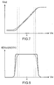
- la figure 7 est une caractéristique décrivant l'évolution de la tension de sortie, en fonction de la tension d'entrée de l'amplificateur,
- la figure 8 est une caractéristique décrivant l'évolution de la dérivée de la tension de sortie, en fonction de la dérivée de la tension d'entrée de l'amplificateur, et
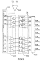
- la figure 9 est un schéma fonctionnel partiel d'un convertisseur analogique/numérique comprenant un amplificateur de tension selon l'invention,
- FIG. 1 is a partial functional diagram of a voltage amplifier according to the invention,
- FIG. 2 is a partial functional diagram of a voltage amplifier according to an advantageous embodiment of the invention,
- FIG. 3 is a set of characteristics describing the evolution of the potentials of the collectors of the first and second transistors, as a function of the input voltage of the amplifier,
- FIG. 4 is a characteristic describing the evolution of the first current added in a portion of the resistive load, as a function of the input voltage of the amplifier,
- FIG. 5 is a characteristic describing the evolution of the second current added in a portion of the resistive load, as a function of the input voltage of the amplifier,
- FIG. 6 is a set of characteristics describing the evolution of the current in said portion of the resistive load, as a function of the input voltage of the amplifier,
- FIG. 7 is a characteristic describing the evolution of the output voltage, as a function of the input voltage of the amplifier,
- FIG. 8 is a characteristic describing the evolution of the derivative of the output voltage, as a function of the derivative of the input voltage of the amplifier, and
- FIG. 9 is a partial functional diagram of an analog / digital converter comprising a voltage amplifier according to the invention,
La figure 1 décrit schématiquement un amplificateur de tension AD selon l'invention. Deux transistors Q1 et Q2 sont montés en paire différentielle : l'émetteur du transistor Q1 est relié à une des bornes d'une résistance, l'émetteur du transistor Q2 étant relié à l'autre borne de la même résistance. Chacun des deux émetteurs est relié à une borne d'une source de courant I1, l'autre borne de ladite source de courant étant reliée à une borne négative d'alimentation, appelée GND. La base du transistor Q1 reçoit la tension d'entrée de l'amplificateur de tension, appelée Vin, la base du transistor Q2 recevant l'opposée de ladite tension d'entrée, soit -Vin. Le collecteur du premier transistor Q1 est relié à une borne positive d'alimentation, appelée VCC, par une première branche comportant une charge résistive, le collecteur du deuxième transistor Q2, fournissant la tension de sortie appelée Vout, étant relié à la borne positive d'alimentation VCC par une deuxième branche comportant une charge résistive. La première branche est formée d'un élément résistif R1. La deuxième branche est formée d'au moins deux éléments résistifs, appelés R21 et R22, montés en série et présentant entre eux au moins un premier noeud intermédiaire, appelé NI, entre la borne positive d'alimentation VCC et le collecteur du deuxième transistor Q2.FIG. 1 schematically describes an amplifier of AD voltage according to the invention. Two transistors Q1 and Q2 are mounted in differential pair: the emitter of transistor Q1 is connected to one of the terminals of a resistor, the emitter of transistor Q2 being connected to the other terminal of the same resistance. Each of the two transmitters is linked to one terminal of a current source I1, the other terminal of said source of current being connected to a negative supply terminal, called GND. The base of transistor Q1 receives the input voltage from the amplifier voltage, called Vin, the base of transistor Q2 receiving the opposite of said input voltage, ie -Vin. The collector of the first transistor Q1 is connected to a positive supply terminal, called VCC, by a first branch comprising a resistive load, the collector of the second transistor Q2, supplying the output voltage called Vout, being connected to the positive VCC supply terminal by a second branch with a resistive load. The first branch is formed a resistive element R1. The second branch is made up of at least two resistive elements, called R21 and R22, connected in series and having between them at least a first intermediate node, called NI, between the positive supply terminal VCC and the collector of the second transistor Q2.
L'amplificateur de tension AD est muni d'une troisième
branche comportant un élément résistif R3 placé en série avec une source
de courant I3, laquelle troisième branche est disposée entre la borne
positive d'alimentation VCC et la borne négative d'alimentation GND et
présente entre l'élément résistif R3 et la source de courant I3 un
deuxième noeud intermédiaire. L'amplificateur de tension est en outre
muni de moyens 10 et 11 pour effectuer une comparaison entre le potentiel
du deuxième noeud intermédiaire, appelé Vref, et celui du collecteur du
premier transistor Q1 d'une part, et entre le potentiel du deuxième noeud
intermédiaire Vref et celui du collecteur du deuxième transistor Q2
d'autre part. Ces mêmes moyens permettent d'ajouter au courant débité
dans une portion de la charge résistive de la deuxième branche, un
premier courant I0 qui s'annule progressivement lorsque le potentiel du
collecteur du premier transistor Q1, appelé VC1, devient inférieur à
Vref, et un second courant I0' qui s'annule progressivement lorsque le
potentiel du collecteur du deuxième transistor Q2, appelé VC2, devient
supérieur à Vref.The AD voltage amplifier has a third
branch comprising a resistive element R3 placed in series with a source
current I3, which third branch is arranged between the terminal
positive supply VCC and the negative supply terminal GND and
between the resistive element R3 and the current source I3 a
second intermediate node. The voltage amplifier is also
provided with
La figure 2 décrit schématiquement un amplificateur de
tension AD selon un mode de réalisation avantageux de l'invention. Les
structures de l'étage amplificateur et des branches comportant les
charges résistives sont identiques à celles décrites par la figure 1. Un
mode de réalisation des moyens 10 et 11 y est en outre exposé : ils
comprennent respectivement un troisième transistor Q3 et un quatrième
transistor Q4, montés en paire différentielle, et un cinquième transistor
Q5 et un sixième transistor Q6, montés en paire différentielle. La base
du troisième transistor Q3 est reliée au collecteur du premier transistor
Q1, celle du quatrième transistor Q4 au deuxième noeud intermédiaire, la
base du cinquième transistor Q5 est reliée au collecteur du deuxième
transistor Q2, celle du sixième transistor Q6 au deuxième noeud
intermédiaire. Les collecteurs des troisième et sixième transistors Q3 et
Q6 sont reliés au premier noeud intermédiaire NI, et ceux des quatrième
et cinquième transistors Q4 et Q5 à la borne positive d'alimentation VCC.FIG. 2 schematically describes an amplifier of
voltage AD according to an advantageous embodiment of the invention. The
amplifier stage structures and branches with
resistive loads are identical to those described in Figure 1. A
embodiment of the
Dans ce mode de réalisation, l'élément résistif R21 et l'élément résistif R3 compris dans la troisième branche ont une valeur voisine, et le courant débité par la source de courant I3 a une valeur voisine de la valeur maximale du courant passant dans le deuxième transistor Q2, laquelle est de l'ordre de 2.I1. En outre, l'élément résistif R21 a une valeur inférieure à celle de l'élément résistif R22. On choisit R21 inférieur à R22/10, de sorte que la chute de tension aux bornes de R21 ne provoque qu'un effet correcteur sur la tension de sortie Vout. Enfin, pour des raisons de symétrie de fonctionnement de l'amplificateur, la valeur de la charge résistive de la première branche R1 est égale à la somme des valeurs des éléments résistifs R21 et R22 composant la charge résistive de la deuxième branche.In this embodiment, the resistive element R21 and the resistive element R3 included in the third branch have a value neighbor, and the current delivered by the current source I3 has a value close to the maximum value of the current flowing in the second transistor Q2, which is of the order of 2.I1. In addition, the element resistive R21 has a value lower than that of the resistive element R22. We choose R21 lower than R22 / 10, so that the voltage drop at terminals of R21 only causes a corrective effect on the output voltage Vout. Finally, for reasons of operating symmetry of the amplifier, the value of the resistive load of the first branch R1 is equal to the sum of the values of the resistive elements R21 and R22 composing the resistive load of the second branch.
Les figures 3 à 7 décrivent l'évolution de divers signaux internes à l'amplificateur AD en fonction de la tension d'entrée de celui-ci, afin de faciliter la compréhension de son fonctionnement.Figures 3 to 7 describe the evolution of various signals internal to the AD amplifier depending on the input voltage of this one, in order to facilitate the comprehension of its operation.
La figure 3 décrit l'évolution des potentiels VC1 et VC2, en
fonction de la tension d'entrée Vin de l'amplificateur AD. Les figures 4
et 5 décrivent l'évolution des premier et deuxième courants,
respectivement I0 et I0', ajoutés dans une portion de la charge
résistive, dans ce cas R21, en fonction de la tension d'entrée Vin de
l'amplificateur AD. La figure 6 décrit l'évolution du courant total dans
ladite portion de la charge résistive R21 en fonction de la tension
d'entrée Vin de l'amplificateur AD. La courbe IR210 y représente le
courant qui circulerait dans la deuxième branche si les moyens 10 et 11
n'existaient pas, c'est-à-dire dans le cas de la paire différentielle
classique. Les courbes en pointillés y représentent les courants qui
circuleraient dans la portion de la charge résistive R21, si, dans un
premier cas, la valeur maximale du courant I0 était ajoutée au courant
IR210, et si, dans un deuxième cas, la valeur maximale du courant I0'
était ajoutée au courant précédemment obtenu. La figure 7 décrit en trait
gras l'évolution de la tension de sortie Vout en fonction de la tension
d'entrée Vin d'un amplificateur selon l'invention, la courbe en trait fin
décrivant, elle, l'évolution de la tension de sortie d'une paire
différentielle classique.Figure 3 describes the evolution of potentials VC1 and VC2, in
function of the input voltage Vin of the amplifier AD. Figures 4
and 5 describe the evolution of the first and second currents,
respectively I0 and I0 ', added in a portion of the load
resistive, in this case R21, as a function of the input voltage Vin of
the AD amplifier. Figure 6 describes the evolution of the total current in
said portion of the resistive load R21 as a function of the voltage
input of the AD amplifier. The IR210 curve represents the
current which would circulate in the second branch if
Lorsque Vin est négatif et grand en valeur absolue, le transistor Q1 est très peu conducteur alors que le transistor Q2 est très conducteur. Le courant dans la première branche est donc très faible, alors que le courant dans la deuxième branche est important. La chute de tension dans l'élément résistif R1 est négligeable, alors que les chutes de tension dans les éléments résistifs R21 et R22 sont significatives. On observe sur la figure 3 que VC1 est alors nettement supérieur à Vref. Le transistor Q4 est donc peu conducteur alors que le transistor Q3 est très conducteur et fait passer un courant I0 au travers de la résistance R21. Vref étant nettement supérieur à VC2, le transistor Q5 est peu conducteur alors que le transistor Q6 est très conducteur et fait passer un courant I0' supplémentaire au travers de la résistance R21. Le courant total IR21 circulant au travers de la résistance R21 est décrit par la figure 6. Le courant circulant dans la deuxième branche étant à son niveau maximal, la tension de sortie Vout est alors à son niveau le plus bas, comme le montre la figure 7, et la chute de tension additionnelle générée dans R21 par les courants ajoutés I0 et I0' explique la différence de valeur entre le niveau bas de la tension de sortie Vout d'un amplificateur selon l'invention et celui de la tension de sortie de la paire différentielle classique.When Vin is negative and large in absolute value, the transistor Q1 is not very conductive while transistor Q2 is very driver. The current in the first branch is therefore very weak, while the current in the second branch is important. The fall of voltage in the resistive element R1 is negligible, while the drops of voltage in the resistive elements R21 and R22 are significant. We observe in FIG. 3 that VC1 is then clearly greater than Vref. The transistor Q4 is therefore not very conductive while transistor Q3 is very conductor and passes a current I0 through the resistor R21. Vref being clearly superior to VC2, the transistor Q5 is not very conductive while the transistor Q6 is very conductive and passes a current Additional I0 'through resistor R21. Total current IR21 flowing through the resistor R21 is described in Figure 6. The current flowing in the second branch being at its maximum level, the output voltage Vout is then at its lowest level, as the shows figure 7, and the additional voltage drop generated in R21 by the added currents I0 and I0 'explains the difference in value between the low level of the output voltage Vout of an amplifier according to the invention and that of the differential pair output voltage classic.
Lorsque Vin augmente, tout en restant négatif, la première zone de fonctionnement non-linéaire de l'étage amplificateur classique est atteinte : le transistor Q1 conduit plus, alors que le transistor Q2 conduit moins, le courant circulant dans la première branche augmente alors que le courant circulant dans la deuxième branche diminue. Les potentiels VC1 et Vref se rapprochent, augmentant la conduction de Q4 et diminuant la conduction de Q3, provoquant l'annulation progressive du courant I0 passant au travers de la résistance R21.When Vin increases, while remaining negative, the first non-linear operating area of the conventional amplifier stage is reached: transistor Q1 conducts more, while transistor Q2 conducts less, the current flowing in the first branch increases while the current flowing in the second branch decreases. The potentials VC1 and Vref get closer, increasing the conduction of Q4 and decreasing the conduction of Q3, causing the progressive cancellation of the current I0 passing through resistor R21.
Tout au long de la portion linéaire, qui correspond au changement de signe de Vin, le transistor Q5 reste peu conducteur alors que le transistor Q6 reste très conducteur, et maintient la circulation du courant I0' au travers de la résistance R21.Throughout the linear portion, which corresponds to change of sign of Vin, the transistor Q5 remains not very conductive then that transistor Q6 remains very conductive, and maintains circulation of the current I0 'through the resistor R21.
Lorsque Vin augmente, la deuxième zone de fonctionnement non-linéaire de l'étage amplificateur classique est atteinte : le transistor Q1 conduit encore plus alors que le transistor Q2 conduit encore moins, le courant circulant dans la première branche augmente alors que le courant circulant dans la deuxième branche diminue. Les potentiels VC2 et Vref se rapprochent, augmentant la conduction de Q5 et diminuant la conduction de Q6, provoquant l'annulation progressive du courant I0' passant au travers de la résistance R21.When Vin increases, the second non-linear operating zone of the classic amplifier stage is reached: the transistor Q1 conducts even more while transistor Q2 conducts even less, the current flowing in the first branch increases while the current flowing in the second branch decreases. VC2 potentials and Vref get closer, increasing the conduction of Q5 and decreasing the conduction of Q6, causing the progressive cancellation of the current I0 ' passing through resistance R21.
Enfin, lorsque Vin est grand, le transistor Q2 est très peu conducteur alors que le transistor Q1 est très conducteur. Le courant dans la deuxième branche est donc très faible, alors que le courant dans la première branche est important. La chute de tension dans l'élément résistif R1 est significative, alors que les chutes de tension dans les éléments résistifs R21 et R22 sont négligeables. La tension de sortie Vout est alors à son niveau le plus haut, comme le montre la figure 7.Finally, when Vin is large, the transistor Q2 is very little conductive while the transistor Q1 is very conductive. The flow in the second branch is therefore very weak, while the current in the first branch is important. Voltage drop in the element resistive R1 is significant, while the voltage drops in the resistive elements R21 and R22 are negligible. The output voltage Vout is then at its highest level, as shown in Figure 7.
Cette figure montre l'influence des paires additionnelles de transistors dans les zones de non-linéarité de la caractéristique de la tension de sortie. En effet, dans la première zone non-linéaire, où Vout augmente trop tôt avec Vin dans le cas de la paire différentielle classique, l'ajout des courants I0 et I0' maintient artificiellement Vout au niveau bas plus longtemps, puis la diminution progressive de I0 permet à Vout d'augmenter quasi-linéairement. De même, dans la deuxième zone non-linéaire, où Vout augmente trop lentement avec Vin dans le cas de la paire différentielle classique, l'ajout du courant I0' maintient artificiellement Vout à un niveau intermédiaire plus longtemps, puis la diminution progressive de I0' permet à Vout d'augmenter quasi-linéairement.This figure shows the influence of the additional pairs of transistors in the areas of non-linearity of the characteristic of the output voltage. Indeed, in the first non-linear zone, where Vout increases too early with Vin in the case of the differential pair classical, the addition of the currents I0 and I0 'artificially maintains Vout at the low level longer, then the gradual decrease in I0 allows Vout to increase almost linearly. Similarly, in the second zone non-linear, where Vout increases too slowly with Vin in the case of classic differential pair, adding the current I0 'maintains artificially Vout at an intermediate level longer then the progressive decrease of I0 'allows Vout to increase almost linearly.
De la sorte, la zone où la tension de sortie évolue linéairement en fonction de la tension d'entrée est élargie. On peut observer ce résultat sur la figure 8, où l'on voit deux caractéristiques d(Vin)/d(Vout) en fonction de la tension d'entrée Vin, l'une en trait fin correspondant à une paire différentielle classique, et l'autre en trait gras correspondant à un amplificateur selon l'invention. La partie "plate", où la dérivée de la tension de sortie Vout par rapport à la tension d'entrée Vin est constante, correspond à la partie où la tension de sortie évolue linéairement en fonction de la tension d'entrée. La zone ainsi délimitée est clairement plus large pour un amplificateur de tension selon l'invention que pour une paire différentielle classique.In this way, the area where the output voltage changes linearly as a function of the input voltage is widened. We can observe this result in figure 8, where we see two characteristics d (Vin) / d (Vout) as a function of the input voltage Vin, one in thin line corresponding to a classic differential pair, and the other in line bold corresponding to an amplifier according to the invention. The part "flat", where the derivative of the output voltage Vout with respect to the input voltage Vin is constant, corresponds to the part where the voltage output changes linearly as a function of the input voltage. The area thus delimited is clearly wider for an amplifier tension according to the invention only for a conventional differential pair.
La figure 9 représente partiellement un convertisseur analogique/numérique qui comporte un amplificateur de tension AD conforme à l'une des variantes représentées sur les figures 1 et 2. Dans le cas présent, ce convertisseur reçoit une tension d'entrée analogique de nature différentielle (Vin, -Vin) à convertir en un signal de sortie numérique codé sur 8 bits Vout(0...7). Ce convertisseur comprend :
- l'amplificateur d'entrée AD recevant la tension d'entrée analogique (Vin, -Vin), et fournissant une tension de sortie analogique,
- une échelle de résistances 100, formée de 64 résistances placées en série entre une borne positive et une borne négative d'alimentation, respectivement Vtop et Vbot, résistances fournissant à leurs noeuds intermédiaires 64 tensions dites de référence, V0, V1,...V63, V0 étant égale à Vbot.
- un étage de comparateurs 200, formé de 64 comparateurs, chacun réalisant la comparaison de la tension de sortie de l'amplificateur d'entrée AD avec l'une des tensions de référence V0, V1,...V63,
- un étage de mémorisation 300 composé d'éléments de mémorisation dits cellules mémoire M0, M1,...M63, chaque cellule mémoire Mi (pour i=0 à 63) étant munie d'une entrée de données, d'une sortie et d'une entrée d'horloge, et recevant sur son entrée de données le signal de sortie Ci d'un comparateur, toutes les cellules mémoire M0, M1,...M63 composant l'étage de mémorisation 300 recevant sur leurs entrées d'horloge un même signal Ck dit signal d'horloge,
- un encodeur binaire 400, lequel encodeur 400 reçoit en entrée les sorties S0, S1,...S63 de l'étage de mémorisation 300 et fournit le signal de sortie numérique du convertisseur Vout(0...7).
- the input amplifier AD receiving the analog input voltage (Vin, -Vin), and supplying an analog output voltage,
- a
resistance scale 100, formed of 64 resistors placed in series between a positive terminal and a negative supply terminal, respectively Vtop and Vbot, resistors supplying their intermediate nodes with 64 so-called reference voltages, V0, V1, ... V63 , V0 being equal to Vbot. - a
comparator stage 200, formed of 64 comparators, each carrying out the comparison of the output voltage of the input amplifier AD with one of the reference voltages V0, V1, ... V63, - a
storage stage 300 composed of storage elements called memory cells M0, M1, ... M63, each memory cell Mi (for i = 0 to 63) being provided with a data input, an output and d 'a clock input, and receiving on its data input the output signal Ci of a comparator, all the memory cells M0, M1, ... M63 composing thestorage stage 300 receiving on their clock inputs the same signal Ck said clock signal, - a
binary encoder 400, which encoder 400 receives as input the outputs S0, S1, ... S63 of thestorage stage 300 and supplies the digital output signal of the converter Vout (0 ... 7).
Claims (7)
- A voltage amplifier intended to receive an input voltage and to supply an output voltage, which voltage amplifier comprises an amplifier stage including a first and a second transistor arranged as a differential pair, the base of the first transistor being intended to receive the input voltage, the base of the second transistor being intended to receive a voltage opposed to said input voltage, the collector of the first transistor being connected to a positive power supply terminal by means of a first branch comprising a resistive load, the collector of the second transistor, intended to supply the output voltage being connected to the positive power supply terminal by means of a second branch comprising a resistive load, characterized in that the second branch is constituted by at least two series-arranged resistive elements having at least a first intermediate node between the positive power supply terminal and the collector of the second transistor, in that said voltage amplifier is provided with a third branch comprising a resistive element arranged in series with a current source, said third branch being arranged between the positive power supply terminal and a negative power supply terminal and featuring a second intermediate node between the resistive element and the current source, and in that the voltage amplifier is provided with means for comparing the potential of the second intermediate node with that of the collector of the first transistor, on the one hand, and the potential of the second intermediate node with that of the collector of the second transistor, on the other hand, and for adding to the current supplied in a portion of the resistive load of the second branch, a first current which is progressively reduced to zero when the potential of the collector of the first transistor falls below that of the second intermediate node, and a second current which is progressively reduced to zero when the potential of the collector of the second transistor exceeds that of the second intermediate node.
- A voltage amplifier as claimed in claim 1, characterized in that the means for comparing the potential of the second intermediate node with that of the collector of the first transistor, on the one hand, and the potential of the second intermediate node with that of the collector of the second transistor, on the other hand, respectively comprise a third and a fourth transistor arranged as a differential pair, on the one hand, and a fifth and a sixth transistor, arranged as a differential pair, on the other hand, the base of the third transistor being connected to the collector of the first transistor and that of the fourth transistor being connected to the second intermediate node, the base of the fifth transistor being connected to the collector of the second transistor and that of the sixth transistor being connected to the second intermediate node, and the collectors of the third and the sixth transistor being connected to the first intermediate node.
- A voltage amplifier as claimed in claim 1 or 2, characterized in that the resistive element between the positive power supply terminal and the first intermediate node and the resistive element comprised in the third branch have substantially the same value, and in that the current supplied by the current source comprised in the third branch has a value substantially equal to the maximum value of the current flowing in the second transistor.
- A voltage amplifier as claimed in any one of claims 1 to 3, characterized in that the resistive element between the first intermediate node and the positive power supply terminal has a value which is lower than that of the resistive element between the first intermediate node and the collector of the second transistor.
- A voltage amplifier as claimed in any one of claims 1 to 4, characterized in that the value of the resistive load of the first branch is equal to the sum of the values of the resistive elements constituting the resistive load of the second branch.
- A voltage amplifier as claimed in any one of claims 1 to 5, characterized in that the resistive elements constituting the load of the amplifier stage are resistors.
- An A/D converter intended to receive an analog input voltage of a differential nature, to be converted into a digital output signal, comprising:characterized in that the input amplifier is an amplifier as claimed in any one of claims 1 to 6.an input amplifier intended to receive the analog input voltage, and to supply an analog output voltage,a resistance ladder arranged in series between a positive and a negative power supply terminal, in which the resistors are intended to supply a plurality of reference voltages at their intermediate nodes,a comparator stage in which each comparator is intended to perform a comparison between the output voltage of the input amplifier and one of the reference voltages,a memory stage intended to store the results of said comparisons, anda binary encoder intended to receive the information stored in the memory stage and to supply the digital output signal of the converter,
Applications Claiming Priority (2)
| Application Number | Priority Date | Filing Date | Title |
|---|---|---|---|
| FR9514130A FR2741759A1 (en) | 1995-11-29 | 1995-11-29 | WIDE VOLTAGE AMPLIFIER RANGE OF VARIATION |
| FR9514130 | 1995-11-29 |
Publications (3)
| Publication Number | Publication Date |
|---|---|
| EP0777321A2 EP0777321A2 (en) | 1997-06-04 |
| EP0777321A3 EP0777321A3 (en) | 1999-09-22 |
| EP0777321B1 true EP0777321B1 (en) | 2001-10-10 |
Family
ID=9484992
Family Applications (1)
| Application Number | Title | Priority Date | Filing Date |
|---|---|---|---|
| EP96203266A Expired - Lifetime EP0777321B1 (en) | 1995-11-29 | 1996-11-21 | Amplification of a voltage having wide variation and A-D converter comprising such an amplifier |
Country Status (6)
| Country | Link |
|---|---|
| US (1) | US5777513A (en) |
| EP (1) | EP0777321B1 (en) |
| JP (1) | JPH09186596A (en) |
| KR (1) | KR970031231A (en) |
| DE (1) | DE69615799T2 (en) |
| FR (1) | FR2741759A1 (en) |
Families Citing this family (3)
| Publication number | Priority date | Publication date | Assignee | Title |
|---|---|---|---|---|
| JP3532365B2 (en) * | 1996-11-15 | 2004-05-31 | 株式会社ルネサステクノロジ | Amplifier circuit |
| US6239655B1 (en) | 1999-04-08 | 2001-05-29 | Peavey Electronics Corporation | Microphone amplifier with digital gain control |
| US20030098744A1 (en) * | 2001-11-29 | 2003-05-29 | Seiichi Banba | Variable gain differential amplifier and multiplication circuit |
Family Cites Families (2)
| Publication number | Priority date | Publication date | Assignee | Title |
|---|---|---|---|---|
| JP2766264B2 (en) * | 1987-10-12 | 1998-06-18 | 株式会社東芝 | Differential amplifier circuit |
| JPH0621817A (en) * | 1992-07-01 | 1994-01-28 | Mitsubishi Electric Corp | Differential amplifier and serial parallel d/a converter |
-
1995
- 1995-11-29 FR FR9514130A patent/FR2741759A1/en not_active Withdrawn
-
1996
- 1996-11-21 EP EP96203266A patent/EP0777321B1/en not_active Expired - Lifetime
- 1996-11-21 DE DE69615799T patent/DE69615799T2/en not_active Expired - Fee Related
- 1996-11-25 US US08/755,685 patent/US5777513A/en not_active Expired - Fee Related
- 1996-11-29 JP JP8319589A patent/JPH09186596A/en active Pending
- 1996-11-29 KR KR1019960059225A patent/KR970031231A/en not_active Application Discontinuation
Also Published As
| Publication number | Publication date |
|---|---|
| DE69615799D1 (en) | 2001-11-15 |
| JPH09186596A (en) | 1997-07-15 |
| EP0777321A2 (en) | 1997-06-04 |
| EP0777321A3 (en) | 1999-09-22 |
| US5777513A (en) | 1998-07-07 |
| KR970031231A (en) | 1997-06-26 |
| FR2741759A1 (en) | 1997-05-30 |
| DE69615799T2 (en) | 2002-05-23 |
Similar Documents
| Publication | Publication Date | Title |
|---|---|---|
| EP0438363B1 (en) | Current measurement circuit in a MOS power transistor | |
| EP0740425B1 (en) | Precision digital-to-analogue converter | |
| EP0658977B1 (en) | Variable gain amplifier | |
| EP0731562A1 (en) | Logic circuit with a differential stage | |
| FR2798791A1 (en) | DIGITAL-TO-ANALOG CONVERTER IN CURRENT | |
| EP1961115B1 (en) | Electronic circuit with compensation of intrinsic offset of differential pairs | |
| EP0777322B1 (en) | Voltage amplifier with wide dynamic range and A/D converter using such amplifier | |
| EP0309365B1 (en) | Adjustable current source and automatic calibration digital/analog converter using such a source | |
| EP0777321B1 (en) | Amplification of a voltage having wide variation and A-D converter comprising such an amplifier | |
| FR2692737A1 (en) | Digital-to-analog converter. | |
| EP2711722B1 (en) | Circuit for measuring differential voltage | |
| CA2547565C (en) | Fast analogue-to-digital converter | |
| EP0200255B1 (en) | Darlington-type switching stage, especially for a memory word line decoder | |
| FR2750549A1 (en) | ANALOG-DIGITAL CONVERTER | |
| EP0453034B1 (en) | Distortion compensated differential circuit | |
| EP1362417B1 (en) | Variable-gain differential input and output amplifier | |
| EP1346475A2 (en) | Controllable set of current sources | |
| EP0467450B1 (en) | Broad band amplifier with separate outputs | |
| EP0203645A1 (en) | Integrated digital-analogous conversion circuit with a glitch reduction device | |
| EP1362419B1 (en) | Normalizing circuit with reduced error voltage | |
| FR2560724A1 (en) | DIGITAL-TO-ANALOG CONVERTER DEVICE | |
| FR2619972A1 (en) | Differential amplifier stage and circuit configurations using such a stage | |
| EP0332499B1 (en) | Fast comparator with an output stage operating in two phases | |
| EP0886382A1 (en) | Analog-to-digital converter | |
| EP0069072A2 (en) | Amplifier circuit |
Legal Events
| Date | Code | Title | Description |
|---|---|---|---|
| PUAI | Public reference made under article 153(3) epc to a published international application that has entered the european phase |
Free format text: ORIGINAL CODE: 0009012 |
|
| AK | Designated contracting states |
Kind code of ref document: A2 Designated state(s): DE FR GB |
|
| RAP3 | Party data changed (applicant data changed or rights of an application transferred) |
Owner name: KONINKLIJKE PHILIPS ELECTRONICS N.V. Owner name: PHILIPS COMPOSANTS ET SEMICONDUCTEURS |
|
| PUAL | Search report despatched |
Free format text: ORIGINAL CODE: 0009013 |
|
| AK | Designated contracting states |
Kind code of ref document: A3 Designated state(s): DE FR GB |
|
| RAP1 | Party data changed (applicant data changed or rights of an application transferred) |
Owner name: KONINKLIJKE PHILIPS ELECTRONICS N.V. |
|
| 17P | Request for examination filed |
Effective date: 20000322 |
|
| GRAG | Despatch of communication of intention to grant |
Free format text: ORIGINAL CODE: EPIDOS AGRA |
|
| 17Q | First examination report despatched |
Effective date: 20001208 |
|
| GRAG | Despatch of communication of intention to grant |
Free format text: ORIGINAL CODE: EPIDOS AGRA |
|
| GRAH | Despatch of communication of intention to grant a patent |
Free format text: ORIGINAL CODE: EPIDOS IGRA |
|
| GRAH | Despatch of communication of intention to grant a patent |
Free format text: ORIGINAL CODE: EPIDOS IGRA |
|
| GRAA | (expected) grant |
Free format text: ORIGINAL CODE: 0009210 |
|
| AK | Designated contracting states |
Kind code of ref document: B1 Designated state(s): DE FR GB |
|
| REF | Corresponds to: |
Ref document number: 69615799 Country of ref document: DE Date of ref document: 20011115 |
|
| PGFP | Annual fee paid to national office [announced via postgrant information from national office to epo] |
Ref country code: FR Payment date: 20011122 Year of fee payment: 6 |
|
| PGFP | Annual fee paid to national office [announced via postgrant information from national office to epo] |
Ref country code: GB Payment date: 20011130 Year of fee payment: 6 |
|
| REG | Reference to a national code |
Ref country code: GB Ref legal event code: IF02 |
|
| GBT | Gb: translation of ep patent filed (gb section 77(6)(a)/1977) |
Effective date: 20011220 |
|
| PGFP | Annual fee paid to national office [announced via postgrant information from national office to epo] |
Ref country code: DE Payment date: 20020116 Year of fee payment: 6 |
|
| PLBE | No opposition filed within time limit |
Free format text: ORIGINAL CODE: 0009261 |
|
| STAA | Information on the status of an ep patent application or granted ep patent |
Free format text: STATUS: NO OPPOSITION FILED WITHIN TIME LIMIT |
|
| 26N | No opposition filed | ||
| PG25 | Lapsed in a contracting state [announced via postgrant information from national office to epo] |
Ref country code: GB Free format text: LAPSE BECAUSE OF NON-PAYMENT OF DUE FEES Effective date: 20021121 |
|
| PG25 | Lapsed in a contracting state [announced via postgrant information from national office to epo] |
Ref country code: DE Free format text: LAPSE BECAUSE OF NON-PAYMENT OF DUE FEES Effective date: 20030603 |
|
| GBPC | Gb: european patent ceased through non-payment of renewal fee | ||
| PG25 | Lapsed in a contracting state [announced via postgrant information from national office to epo] |
Ref country code: FR Free format text: LAPSE BECAUSE OF NON-PAYMENT OF DUE FEES Effective date: 20030731 |
|
| REG | Reference to a national code |
Ref country code: FR Ref legal event code: ST |