EP0776554B1 - Optischer emissionskopf mit laser und modulator - Google Patents
Optischer emissionskopf mit laser und modulator Download PDFInfo
- Publication number
- EP0776554B1 EP0776554B1 EP95926988A EP95926988A EP0776554B1 EP 0776554 B1 EP0776554 B1 EP 0776554B1 EP 95926988 A EP95926988 A EP 95926988A EP 95926988 A EP95926988 A EP 95926988A EP 0776554 B1 EP0776554 B1 EP 0776554B1
- Authority
- EP
- European Patent Office
- Prior art keywords
- signal
- optical
- electrical
- modulator
- modulating
- Prior art date
- Legal status (The legal status is an assumption and is not a legal conclusion. Google has not performed a legal analysis and makes no representation as to the accuracy of the status listed.)
- Expired - Lifetime
Links
- 230000003287 optical effect Effects 0.000 title claims description 104
- 230000010363 phase shift Effects 0.000 claims description 10
- 238000001914 filtration Methods 0.000 claims description 9
- 230000008878 coupling Effects 0.000 claims description 6
- 238000010168 coupling process Methods 0.000 claims description 6
- 238000005859 coupling reaction Methods 0.000 claims description 6
- 238000010079 rubber tapping Methods 0.000 claims 5
- 230000001131 transforming effect Effects 0.000 claims 5
- 238000001228 spectrum Methods 0.000 description 10
- 239000013307 optical fiber Substances 0.000 description 9
- 230000005540 biological transmission Effects 0.000 description 7
- 229910052691 Erbium Inorganic materials 0.000 description 5
- 238000003780 insertion Methods 0.000 description 5
- 230000037431 insertion Effects 0.000 description 5
- 230000033228 biological regulation Effects 0.000 description 4
- 239000000969 carrier Substances 0.000 description 4
- 230000000295 complement effect Effects 0.000 description 3
- 230000000875 corresponding effect Effects 0.000 description 3
- 239000000835 fiber Substances 0.000 description 2
- 230000006872 improvement Effects 0.000 description 2
- 230000010287 polarization Effects 0.000 description 2
- 230000001105 regulatory effect Effects 0.000 description 2
- JBRZTFJDHDCESZ-UHFFFAOYSA-N AsGa Chemical compound [As]#[Ga] JBRZTFJDHDCESZ-UHFFFAOYSA-N 0.000 description 1
- 229910001218 Gallium arsenide Inorganic materials 0.000 description 1
- 230000009471 action Effects 0.000 description 1
- 230000032683 aging Effects 0.000 description 1
- 230000015556 catabolic process Effects 0.000 description 1
- 238000012885 constant function Methods 0.000 description 1
- 239000000470 constituent Substances 0.000 description 1
- 230000002596 correlated effect Effects 0.000 description 1
- 238000006731 degradation reaction Methods 0.000 description 1
- 238000010586 diagram Methods 0.000 description 1
- 239000006185 dispersion Substances 0.000 description 1
- 230000000694 effects Effects 0.000 description 1
- 238000005516 engineering process Methods 0.000 description 1
- 239000000284 extract Substances 0.000 description 1
- 238000012423 maintenance Methods 0.000 description 1
- 230000005693 optoelectronics Effects 0.000 description 1
- 230000009467 reduction Effects 0.000 description 1
- 230000004044 response Effects 0.000 description 1
- 230000008054 signal transmission Effects 0.000 description 1
- 230000009466 transformation Effects 0.000 description 1
- 238000011144 upstream manufacturing Methods 0.000 description 1
Images


Classifications
-
- H—ELECTRICITY
- H04—ELECTRIC COMMUNICATION TECHNIQUE
- H04B—TRANSMISSION
- H04B10/00—Transmission systems employing electromagnetic waves other than radio-waves, e.g. infrared, visible or ultraviolet light, or employing corpuscular radiation, e.g. quantum communication
- H04B10/50—Transmitters
- H04B10/501—Structural aspects
- H04B10/503—Laser transmitters
- H04B10/505—Laser transmitters using external modulation
- H04B10/5057—Laser transmitters using external modulation using a feedback signal generated by analysing the optical output
- H04B10/50577—Laser transmitters using external modulation using a feedback signal generated by analysing the optical output to control the phase of the modulating signal
-
- H—ELECTRICITY
- H04—ELECTRIC COMMUNICATION TECHNIQUE
- H04B—TRANSMISSION
- H04B10/00—Transmission systems employing electromagnetic waves other than radio-waves, e.g. infrared, visible or ultraviolet light, or employing corpuscular radiation, e.g. quantum communication
- H04B10/50—Transmitters
- H04B10/501—Structural aspects
- H04B10/503—Laser transmitters
- H04B10/505—Laser transmitters using external modulation
- H04B10/5059—Laser transmitters using external modulation using a feed-forward signal generated by analysing the optical or electrical input
- H04B10/50593—Laser transmitters using external modulation using a feed-forward signal generated by analysing the optical or electrical input to control the modulating signal amplitude including amplitude distortion
Definitions
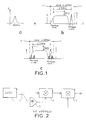
- the invention relates to the transmission of analog signals over optical fiber and more particularly the association of a laser with a modulator optics to achieve this.
- the modulation input of the optical modulator receives a signal consisting of one or more carriers, for example amplitude modulated.
- An example of this signal represented in FIG. 1b, consists of a audio and video carrier, the frequency spectrum of the video carrier corresponding to amplitude modulation with residual sideband called MA-BLR.
- These 2 modulated carriers represent a channel in the area of television signal transmissions, and the signal of modulation transmitted to the optical modulator can consist of a set of adjacent channels to constitute a frequency multiplex multichannel sideband amplitude modulated television signals residual.
- the multiplication of the optical signal with this modulation signal RF transposes the noise of the laser around the carriers of the RF signal as shown in Figure 1c.
- This noise is found in the frequency bands lateral if these have a width greater than a few tens of kilohertz as is the case for the video modulation signal.
- the baseband video signal is in the presence of double power noise since the two "lines” of noise around the video carrier are correlated while the spectrum of the video signal is at reduced side band. This noise level then exceeds the visibility threshold video signal on the screen of up to 10 or 12 dB, thus creating a "pencil" effect on the image.
- a solution to this problem is known for example from the document: Progress in Externally Modulated AM CATV Transmission Systems, NAZARTHY et al., Journal of Lightwave Technology, vol. 11, January 1993 p. 82-105.
- This is to insert, between the laser and the modulator external, a device for regulating the transmitted power.
- This device is shown in Figure 2.
- a coupler 2 takes part of the power at the output of the laser 1 to transmit it to an optical receiver 3 with integrated amplifier which converts this optical signal into an electrical signal which will control a first external optical modulator 4 which plays the role regulator.
- a suitable choice of receiver coupling and gain values optics effectively reduce laser noise before the beam is not transmitted to the second external optical modulator 5 receiving RF modulation signals.
- a first drawback to this solution concerns losses insertion of the coupler and the optical regulation modulator which reduce strongly the usable optical power of the laser, the optical modulator, by its principle, dividing the power by two.
- the output power available from the regulation principle is at most equal to the minimum power value wave delivered by the laser.
- Another disadvantage concerns the setting in point of the device, the gain of the regulatory chain symbolized by the optical receiver 3 to be precisely adjusted, the correction signal must be perfectly in phase with the noise to be corrected.
- the optical modulator necessary for power regulation is costly not negligible.
- the invention aims to overcome the aforementioned drawbacks.
- an optical transmission head composed of a laser emitting a signal of average light power Po and of instantaneous power Po (1 + e), e being the superimposed noise power to the signal and related to the average power Po, and a modulator external optics to modulate the optical signal from the laser from of an electrical modulation signal M, characterized in that the signal of modulation M 'applied directly to the optical modulator is a signal electric proportional to M (1-e).
- the present invention overcomes the disadvantages due to the variation of the laser wavelength, by the use of a external laser optical modulator. It also makes it possible to limit the insertion losses, compared to a power regulation device of "Feed-Forward" type. In addition, its cost of realization and implementation is more reduced.
- the effective modulation signal M ' is produced from a electric modulator receiving an original modulation signal M and a modulation control signal C.
- the electric modulator can supply either a signal proportional to CM, or a signal of the form K2CM + K3M K2 and K3 being constants.
- the signal C must be proportional to (1 - e); in the second case the signal C can be proportional to e.
- To produce the signal C we take part of the instantaneous optical power either directly at the laser output or at the optical modulator output.
- the output corresponding to the channel main of this coupler is transmitted directly, through an optical fiber, at the input of an optical modulator 8 whose function is receive a radio frequency electrical signal to modulate the power optical depending on this electrical signal.
- an optical modulator 8 whose function is receive a radio frequency electrical signal to modulate the power optical depending on this electrical signal.
- M represents the desired modulation rate, between - 1/2 and + 1/2. This modulation rate is represented by the variations of a radio frequency signal applied to the device, which signal will be designated also by M.
- the output corresponding to the coupled channel is connected, always by through an optical fiber, to an optical receiver 9 which transforms optical signals into electrical signals.
- the electrical signal available at the output of the receiver 9 is proportional to the power emitted from the laser Pi.
- the power Pi emitted by the laser is of the form Po (1 + e).
- the electrical signal at the output of the optical receiver is equal to KP o (1 + e), K being a constant function of the coupling coefficient of the optical coupler 7, of the losses in the optical fiber connected to the optical receiver and of the transformation coefficient of the optical power in electrical voltage of the optical receiver.
- K being a constant function of the coupling coefficient of the optical coupler 7, of the losses in the optical fiber connected to the optical receiver and of the transformation coefficient of the optical power in electrical voltage of the optical receiver.
- the assembly of the optical receiver 9 and the amplifier 10 has a bandwidth such that the frequencies of variations in instantaneous power (a few hundred kHz for example) are preserved.
- the subtractor 11 is easily produced by applying a offset voltage at amplifier 10.
- the signal C supplies the modulation input of an electrical modulator 12 of the multiplier type, the signal of which to be modulated M is transmitted on a second input.
- This signal M is for example constituted by radio frequency signals RF from television, which are multiplexed frequently, of the type described in FIG. 1b.
- Co is the value of signal C when the instantaneous power Pi is equal to the average power Po and in this case the modulation signal effective M 'is equal to the signal M representing the desired modulation.
- This signal M ' is transmitted to the optical modulator 8 on its modulation input.
- This modulator generally has 2 complementary optical outputs, P + and P - , each of power half the input power for zero modulation.
- this device assumes that the average power Po is fixed, the gain of amplifier 10 being calculated as a function of Po.
- an improvement of the device consists in measuring this average power Po from a low-pass filter, eliminating instantaneous power fluctuations, to control the gain of amplifier 10 as a function of this value.
- This improvement is shown in dotted lines in FIG. 3 and consists in taking the signal in output of the optical receiver 9 to make it pass through a low-pass filter 13, cutoff frequency for example of the order of a kiloherz to eliminate the noise spectrum, then control the gain of amplifier 10 by connecting the output of this filter at the gain control input of amplifier 10.
- the necessary phase adjustment between the signal of noise e contained in the laser signal to be modulated and that of the signal modulation M ' is here achieved by adapting the length of the fibers optical; but a phase shifting circuit could also be used.
- a laser 14 is connected by optical fiber to an optical modulator 15.
- an optical coupler 16 which collects a small part of the optical signal to transmit it, via an optical fiber connected to its coupled output, to an optical receiver 17 consisting of an optoelectronic transducer.
- An amplifier 18 connected at its output amplifies and filters the electrical signal.
- This amplifier is connected to a phase shifter 19 whose output provides a modulation signal C to an electric modulator 20.
- This modulator 20 receives on a second input the signal M to be modulated and provides at its output the modulated signal M 'which is sent to the modulation input of the optical modulator 15.
- the amplifier 18 extracts the noise from the laser e which is in the low frequencies and which crosses the optical modulator, to modulate the signal M and supply a new modulation signal M 'of the form M (1-e), such a signal limiting the degradation of the modulating signal M by the noise of the laser as previously indicated.
- the amplifier 18 can be produced so that its transfer resistance R T is inversely proportional to Po.
- Signal C actually corresponds to signal S after phase shift.
- the phase shift circuit 19 makes it possible to maintain the phase condition between the correction signal C transmitted to the electric modulator and the signal to be corrected, that is to say a zero phase shift between the noise signal e contained in the signal P - and the correction signal C; the phase shifter performs a phase shift which, associated with a phase inversion in the optical receiver and phase shift due to the loop, causes a phase shift of 360 ° in the vicinity of the frequency of the peak of the relaxation noise spectrum which is a narrow spectrum around of 200 KHz in the case of a Glass-Erbium type laser.
- the delay time in the loop is around 150 ns, which corresponds to a phase shift of around ten degrees for a signal at the frequency of 200 KHz.
- the phase shift produced by the phase shifter 19 is of the order of 170 °.
- the latter must be aperiodic with respect to the modulation signal, that is to say that its action on the RF signal should not depend on the RF frequency.
- the choice of a optical modulator with two complementary outputs is not essential for the realization of the invention, although it allows simultaneously supply two series of subscribers to a network, for example of optical transmission by cable by the simultaneous exploitation of these two exits.
- the coupling enabling the optical receiver and the electric modulator can, of course, be made indifferently on one of these two outputs.
- an optical receiver + amplifier receiving the optical signal from the optical coupler and comprising a photodiode and an amplifier with variable resistance for adjusting the gain of the loop
- a phase shifter comprising a circuit inverter followed by 2 complementary transistor circuits with resistance adjustable for setting the desired phase shift then a modulator electric consisting of an FET transistor with gallium arsenide acting as variable resistance.
- the original modulation signal is transmitted on the RF input and the RF output is connected to the input of the optical modulator.
Landscapes
- Physics & Mathematics (AREA)
- Optics & Photonics (AREA)
- Electromagnetism (AREA)
- Engineering & Computer Science (AREA)
- Computer Networks & Wireless Communication (AREA)
- Signal Processing (AREA)
- Optical Communication System (AREA)
Claims (10)
- Optischer Emissionskopf mit einem Laser (6, 14), der ein Signal mit der mittleren Lichtleistung Po und der momentanten Leistung Po (1+e) aussendet, wobei e die dem Signal überlagerte Rauschleistung ist, bezogen auf die mittlere Leistung Po, und mit einem externen optischen Modulator (8, 15) zum Modulieren des von dem Laser aufgrund eines elektrischen Modulationssignals M gelieferten optischen Signals, dadurch gekennzeichnet, daß das dem optischen Modulator (8, 15) unmittelbar zugeführte Modulationssignal F' ein zu M(1-e) proportionales elektrisches Signal ist.
- Optischer Emissionskopf nach Anspruch 1, dadurch gekennzeichnet, daß das Modulationssignal M zur Bildung des Signals M' über einen elektrischen Modulator (12, 20) geführt ist, dessem Modulationseingang ein elektrisches Signal C zugeführt ist, das aus dem optischen Signal gewonnen ist und dessen modulierte Ausgangsspannung M' proportional zu CM ist.
- Optischer Emissionskopf nach Anspruch 1, dadurch gekennzeichnet, daß das Modulationssignal M zur Bildung des Signals M' über einen elektrischen Modulator (12, 20) geführt ist, dessem Modulationseingang ein aus dem optischen Signal gewonnenes elektrisches Signal C zugeführt ist und dessen modulierte Ausgangsspannung M' die Form M' = K2 CM + K3 M hat, wobei K2 und K3 Konstanten sind.
- Optischer Emissionskopf nach Anspruch 3, dadurch gekennzeichnet, daß das elektrische Signal C mittels eines optischen Koppelgliedes (7) gebildet wird, das an den Ausgang des Lasers (6) angeschlossen ist, um dem optischen Empfänger (9) ein optisches Signal zu entnehmen und dieses entnommene optische Signal in ein elektrisches Signal umzusetzen, derart, daß das gewonnene Signal proportional zu Po (1+e) ist, sowie mit einem Filter zur Beseitigung der Gleichspannungskomponente in dem elektrischen Signal und mit einem Verstärker (10) mit einer zu Po umgekehrt proportionalen Verstärkung zur Verstärkung des elektrischen Signals vor oder nach der Filterung.
- Optischer Emissionskopf nach Anspruch 2 oder 3, dadurch gekennzeichnet, daß das elektrische Signal C mittels eines an den Ausgang des Lasers (6) angeschlossenen optischen Koppelelementes (7) zur Entnahme eines optischen Signals gewonnen ist, sowie mit einem optischen Empfänger (9) zum Umsetzen des entnommenen optischen Signal in ein elektrisches Signal, derart, daß das gewonnene Signal proportional zu Po (1+e) ist, und mit einem Verstärker (10) mit einer zu Po umgekehrt proportionalen Verstärkung zum Verstärken des Signals von dem optischen Empfänger (9) und mit einer Subtrahierstufe (11) zum Subtrahieren des verstärkten Signals von einem Referenzwert.
- Optischer Emissionskopf nach Anspruch 2 oder 3, dadurch gekennzeichnet, daß das elektrische Modulationssignal C durch ein optisches Koppelelement (16) gewonnen wird, das an den Ausgang des optischen Modulators (15) angeschlossen ist, um ein optisches Signal zu entnehmen, sowie mit einem optischen Empfänger (17) zum Umsetzen des entnommenen optischen Signals in ein elektrisches Signal, und mit einem Filter zum Extrahieren der Komponente Po (1+e) aus dem elektrischen Signal und zum Unterdrücken der Komponenten bei den Modulationsfrequenzen und mit einem Verstärker mit einer zu Po umgekehrt proportionalen Verstärkung zur Verstärkung des Signals vor oder nach der Filterung und schließlich mit einer Subtrahierstufe zum Subtrahieren dieses verstärkten und gefilterten Signals von einem Referenzwert.
- Optischer Emissionskopf nach Anspruch 3, dadurch gekennzeichnet, daß das elektrische Modulationssignal C mittels eines optischen Kopplungselementes (16), das an den Ausgang des optischen Modulators (15) zur Entnahme eines optischen Signals angeschlossen ist, mittels eines optischen Empfängers (17) zum Umsetzen des entnommenen optischen Signals in ein elektrisches Signal, mittels eines Filters zum Unterdrücken der Komponenten mit den Modulationsfrequenzen in dem elektrischen Signal und der Gleichspannungskomponente und mittels eines Verstärkers mit einer zu Po umgekehrt proportionalen Verstärkung zur Verstärkung des gewonnenen elektrischen Signals vor oder nach der Filterung erzeugt wird.
- Optischer Emissionskopf nach Anspruch 4, 5, 6 oder 7, dadurch gekennzeichnet, daß
die Verstärkung des Verstärkers (10) durch das Ausgangssignal eines Tiefpaßfilters (13) gesteuert wird, das parallel zum Ausgang des optischen Empfäners (9) liegt und eine derartige Grenzfrequenz hat, daß die dem Signal e entsprechenden Frequenzen des Rauschens unterdrückt werden, um eine der mittleren Leistung Po des Lasers proportionale Ausgangsspannung zu erzeugen. - Optischer Emissionskopf nach Anspruch 7, dadurch gekennzeichnet, daß das elektrische Modulationssignal C mittels eines optischen Koppelelementes (16) mit einem Kopplungsfaktor K1, das an den Ausgang des optischen Modulators (15) zur Entnahme eines optischen Signals angeschlossen ist, und mittels eines optischen Empfängers (17) mit dem Wirkungsgrad h, der mit einem Verstärker (18) mit Filterung mit dem Übertragungswiderstand RT zur Umsetzung des optischen Signals von dem Koppelausgang des optischen Koppelelementes (16) in ein elektrisches Signal verbunden ist, erzeugt wird, wobei der Verstärker und das Filter so ausgebildet sind, daß die Gleichspannungskomponente und die Komponenten der Frequenzen des entnommenen Modulationssignals unterdrückt werden, um nur das Rauschsignal bei diesen Frequenzen zu erhalten, wobei das Koppelement (16), der optische Empfänger (17), der Verstärker (18) und der elektrische Modulator (20) folgende Gleichung erfüllen:
- Optischer Emissionskopf nach den Ansprüchen 4, 5, 6, 7, 8 oder 9, dadurch gekennzeichent, daß ein Phasenschieber (19) zwischen dem Ausgang des optischen Empfängers (9, 17) und dem Modulationseingang des elektrischen Modulators (12, 20) liegt, um eine solche Phasenschiebung zu bilden, daß die Rauschkomponenten des Modulationssignals M' und des optischen Signals am Eingang des optischen Modulators (15) entgegengesetzte Phase haben.
Applications Claiming Priority (3)
| Application Number | Priority Date | Filing Date | Title |
|---|---|---|---|
| FR9410153A FR2723803B1 (fr) | 1994-08-19 | 1994-08-19 | Tete d'emission optique avec laser et modulateur |
| FR9410153 | 1994-08-19 | ||
| PCT/FR1995/001018 WO1996006488A1 (fr) | 1994-08-19 | 1995-07-28 | Tete d'emission optique avec laser et modulateur |
Publications (2)
| Publication Number | Publication Date |
|---|---|
| EP0776554A1 EP0776554A1 (de) | 1997-06-04 |
| EP0776554B1 true EP0776554B1 (de) | 1998-10-21 |
Family
ID=9466400
Family Applications (1)
| Application Number | Title | Priority Date | Filing Date |
|---|---|---|---|
| EP95926988A Expired - Lifetime EP0776554B1 (de) | 1994-08-19 | 1995-07-28 | Optischer emissionskopf mit laser und modulator |
Country Status (6)
| Country | Link |
|---|---|
| US (1) | US6005701A (de) |
| EP (1) | EP0776554B1 (de) |
| JP (1) | JP3591839B2 (de) |
| DE (1) | DE69505544T2 (de) |
| FR (1) | FR2723803B1 (de) |
| WO (1) | WO1996006488A1 (de) |
Families Citing this family (6)
| Publication number | Priority date | Publication date | Assignee | Title |
|---|---|---|---|---|
| JPH11344689A (ja) * | 1998-06-03 | 1999-12-14 | Hitachi Ltd | 固体レーザ装置 |
| US6292598B1 (en) * | 1998-11-04 | 2001-09-18 | Corvis Corporation | Optical transmission apparatuses, methods, and systems |
| US6529305B1 (en) | 1998-11-04 | 2003-03-04 | Corvis Corporation | Optical transmission apparatuses, methods, and systems |
| US6118566A (en) | 1998-11-04 | 2000-09-12 | Corvis Corporation | Optical upconverter apparatuses, methods, and systems |
| US7142788B2 (en) * | 2002-04-16 | 2006-11-28 | Corvis Corporation | Optical communications systems, devices, and methods |
| WO2006051849A1 (ja) * | 2004-11-11 | 2006-05-18 | Nippon Telegraph And Telephone Corporation | 光送信装置、光伝送システム、光送信方法および光伝送方法 |
Family Cites Families (4)
| Publication number | Priority date | Publication date | Assignee | Title |
|---|---|---|---|---|
| US5166509A (en) * | 1990-11-09 | 1992-11-24 | Tacan Corporation | Optical modulator noise nonlinearity reduction circuit |
| NL9002596A (nl) * | 1990-11-28 | 1992-06-16 | Nederland Ptt | Optisch transmissiesysteem voor het overdragen van analoge signalen. |
| JP2711773B2 (ja) * | 1992-02-03 | 1998-02-10 | 国際電信電話株式会社 | 光波形整形装置 |
| US5359450A (en) * | 1992-06-25 | 1994-10-25 | Synchronous Communications, Inc. | Optical transmission system |
-
1994
- 1994-08-19 FR FR9410153A patent/FR2723803B1/fr not_active Expired - Fee Related
-
1995
- 1995-07-28 DE DE69505544T patent/DE69505544T2/de not_active Expired - Lifetime
- 1995-07-28 JP JP50781996A patent/JP3591839B2/ja not_active Expired - Lifetime
- 1995-07-28 EP EP95926988A patent/EP0776554B1/de not_active Expired - Lifetime
- 1995-07-28 US US08/776,604 patent/US6005701A/en not_active Expired - Lifetime
- 1995-07-28 WO PCT/FR1995/001018 patent/WO1996006488A1/fr not_active Ceased
Also Published As
| Publication number | Publication date |
|---|---|
| JP3591839B2 (ja) | 2004-11-24 |
| FR2723803B1 (fr) | 1997-01-03 |
| WO1996006488A1 (fr) | 1996-02-29 |
| EP0776554A1 (de) | 1997-06-04 |
| JPH10511186A (ja) | 1998-10-27 |
| DE69505544T2 (de) | 1999-05-06 |
| US6005701A (en) | 1999-12-21 |
| FR2723803A1 (fr) | 1996-02-23 |
| DE69505544D1 (de) | 1998-11-26 |
Similar Documents
| Publication | Publication Date | Title |
|---|---|---|
| FR2685834A1 (fr) | Systeme de transmission numerique longue distance sur fibre optique a compensation a l'emission des distorsions. | |
| FR2711811A1 (fr) | Amplificateur optique à gain commandable et applications d'un tel amplificateur. | |
| FR2685835A1 (fr) | Systeme de transmission tres longue distance sur fibre optique a compensation des distorsions a la reception. | |
| FR2774483A1 (fr) | Systeme d'egalisation de gain | |
| FR2731525A1 (fr) | Amplificateur optique a gain commandable et procede de commande d'un gain optique | |
| FR2775856A1 (fr) | Systeme et terminal de multiplexage en longueur d'onde optique | |
| FR2526554A1 (fr) | Procede de regulation de moyens emetteurs d'informations lumineuses et le systeme de mise en oeuvre | |
| FR2750552A1 (fr) | Recepteur pour systeme de transmission de signaux numeriques par voie optique | |
| CA2276905A1 (fr) | Amplification quasi-distribuee dans un systeme de transmission a fibre optique a signaux solitons | |
| EP0776554B1 (de) | Optischer emissionskopf mit laser und modulator | |
| EP0881790B1 (de) | Optisches Übertragungssystem mit dynamischer Kompensation der übertragenen Leistung | |
| US11075698B2 (en) | Optical communication system | |
| FR2690294A1 (fr) | Source d'impulsion optique et système de transmission optique à solitons comportant cette source. | |
| EP1526662A2 (de) | Verfahren und Vorrichtung zur Überwachungssignalmodulation mit variablem optischem Dämpfungsglied | |
| US20080112706A1 (en) | Optical receiving apparatus and optical communication system using same | |
| EP0598651B1 (de) | Optisches Übertragungssystem, insbesondere für ein Videokommunikationskabelnetzwerk | |
| EP0560659B1 (de) | Verfahren und Vorrichtung zur optischen Übertragung eines Multiplexsignals mit elektrischen Trägern | |
| WO1997003488A1 (fr) | Source de lumiere a spectre large stabilise et gyroscope a fibre optique associe | |
| FR2712096A1 (fr) | Amplificateur optique, émetteur optique, récepteur optique, leur procédé de commande et procédé pour transmettre un signal de contrôle. | |
| EP0975106B1 (de) | Anordnung zum Inline-Regenerieren eines optischen Solitonsignals durch synchrone Modulation dieser Solitonen und Übertragungssystem mit einer derartigen Vorrichtung | |
| EP0961422B1 (de) | Optischer Sender mit mehreren optischen Quellen | |
| FR2749114A1 (fr) | Systeme de communication optique a amplificateurs optiques dont le gain depend de la polarisation du signal d'entree | |
| EP0849898B1 (de) | Zwischenverstärker für ein faseroptisches Solitonübertragungssystem | |
| EP0532400A1 (de) | Diskriminator mit einer reduzierten Frequenzcharakteristik | |
| FR2524230A1 (fr) | Systeme de transmission d'informations sur une voie de service du type fibre optique |
Legal Events
| Date | Code | Title | Description |
|---|---|---|---|
| PUAI | Public reference made under article 153(3) epc to a published international application that has entered the european phase |
Free format text: ORIGINAL CODE: 0009012 |
|
| 17P | Request for examination filed |
Effective date: 19970207 |
|
| AK | Designated contracting states |
Kind code of ref document: A1 Designated state(s): DE FR GB IT |
|
| GRAG | Despatch of communication of intention to grant |
Free format text: ORIGINAL CODE: EPIDOS AGRA |
|
| 17Q | First examination report despatched |
Effective date: 19971218 |
|
| GRAG | Despatch of communication of intention to grant |
Free format text: ORIGINAL CODE: EPIDOS AGRA |
|
| GRAH | Despatch of communication of intention to grant a patent |
Free format text: ORIGINAL CODE: EPIDOS IGRA |
|
| GRAH | Despatch of communication of intention to grant a patent |
Free format text: ORIGINAL CODE: EPIDOS IGRA |
|
| GRAA | (expected) grant |
Free format text: ORIGINAL CODE: 0009210 |
|
| AK | Designated contracting states |
Kind code of ref document: B1 Designated state(s): DE FR GB IT |
|
| REF | Corresponds to: |
Ref document number: 69505544 Country of ref document: DE Date of ref document: 19981126 |
|
| GBT | Gb: translation of ep patent filed (gb section 77(6)(a)/1977) |
Effective date: 19990201 |
|
| PLBE | No opposition filed within time limit |
Free format text: ORIGINAL CODE: 0009261 |
|
| STAA | Information on the status of an ep patent application or granted ep patent |
Free format text: STATUS: NO OPPOSITION FILED WITHIN TIME LIMIT |
|
| 26N | No opposition filed | ||
| REG | Reference to a national code |
Ref country code: GB Ref legal event code: IF02 |
|
| REG | Reference to a national code |
Ref country code: DE Ref legal event code: R081 Ref document number: 69505544 Country of ref document: DE Owner name: THOMSON LICENSING, FR Free format text: FORMER OWNER: THOMSON-CSF, PARIS, FR Effective date: 20110503 |
|
| PGFP | Annual fee paid to national office [announced via postgrant information from national office to epo] |
Ref country code: IT Payment date: 20120724 Year of fee payment: 18 |
|
| PG25 | Lapsed in a contracting state [announced via postgrant information from national office to epo] |
Ref country code: IT Free format text: LAPSE BECAUSE OF NON-PAYMENT OF DUE FEES Effective date: 20130728 |
|
| PGFP | Annual fee paid to national office [announced via postgrant information from national office to epo] |
Ref country code: DE Payment date: 20140729 Year of fee payment: 20 |
|
| PGFP | Annual fee paid to national office [announced via postgrant information from national office to epo] |
Ref country code: GB Payment date: 20140729 Year of fee payment: 20 Ref country code: FR Payment date: 20140717 Year of fee payment: 20 |
|
| REG | Reference to a national code |
Ref country code: DE Ref legal event code: R071 Ref document number: 69505544 Country of ref document: DE |
|
| REG | Reference to a national code |
Ref country code: GB Ref legal event code: PE20 Expiry date: 20150727 |
|
| PG25 | Lapsed in a contracting state [announced via postgrant information from national office to epo] |
Ref country code: GB Free format text: LAPSE BECAUSE OF EXPIRATION OF PROTECTION Effective date: 20150727 |