EP0774784A2 - Semiconductor integrated circuit device including protection means - Google Patents
Semiconductor integrated circuit device including protection means Download PDFInfo
- Publication number
- EP0774784A2 EP0774784A2 EP96118277A EP96118277A EP0774784A2 EP 0774784 A2 EP0774784 A2 EP 0774784A2 EP 96118277 A EP96118277 A EP 96118277A EP 96118277 A EP96118277 A EP 96118277A EP 0774784 A2 EP0774784 A2 EP 0774784A2
- Authority
- EP
- European Patent Office
- Prior art keywords
- terminal
- protection element
- power source
- semiconductor integrated
- integrated circuit
- Prior art date
- Legal status (The legal status is an assumption and is not a legal conclusion. Google has not performed a legal analysis and makes no representation as to the accuracy of the status listed.)
- Withdrawn
Links
Images

Classifications
-
- H—ELECTRICITY
- H10—SEMICONDUCTOR DEVICES; ELECTRIC SOLID-STATE DEVICES NOT OTHERWISE PROVIDED FOR
- H10D—INORGANIC ELECTRIC SEMICONDUCTOR DEVICES
- H10D84/00—Integrated devices formed in or on semiconductor substrates that comprise only semiconducting layers, e.g. on Si wafers or on GaAs-on-Si wafers
-
- H—ELECTRICITY
- H10—SEMICONDUCTOR DEVICES; ELECTRIC SOLID-STATE DEVICES NOT OTHERWISE PROVIDED FOR
- H10D—INORGANIC ELECTRIC SEMICONDUCTOR DEVICES
- H10D89/00—Aspects of integrated devices not covered by groups H10D84/00 - H10D88/00
- H10D89/60—Integrated devices comprising arrangements for electrical or thermal protection, e.g. protection circuits against electrostatic discharge [ESD]
- H10D89/601—Integrated devices comprising arrangements for electrical or thermal protection, e.g. protection circuits against electrostatic discharge [ESD] for devices having insulated gate electrodes, e.g. for IGFETs or IGBTs
- H10D89/711—Integrated devices comprising arrangements for electrical or thermal protection, e.g. protection circuits against electrostatic discharge [ESD] for devices having insulated gate electrodes, e.g. for IGFETs or IGBTs using bipolar transistors as protective elements
Definitions
- the present invention relates generally to a semiconductor integrated circuit device. More specifically, the invention relates to a semiconductor integrated circuit device with improved electrostatic break down voltage.
- LSI semiconductor integrated circuit device
- electrostatic break down voltage associating with increasing of package density becomes a problem, and various measure for protection has been taken.
- a construction in which a diode for grounding an excessive voltage to a substrate is connected in paralle to an input/output circuit arranged between input/output terminals and an internal circuit is employed.
- a current limiting resistor is connected in series to the input/output circuit.
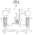
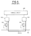
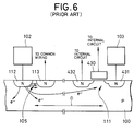
- Figs. 4 to 6 are example of the electrostatic break down protection circuit externally connected to such input/output circuit, in which Fig. 4 is a plan view, Fig. 5 is a circuit diagram of Fig. 4 and Fig. 6 is a section taken along line A - A of Fig. 4.
- an input terminal 102 and a GND (ground) terminal 103 are connected to an internal circuit 420 formed in a P-type semiconductor substrate 100 forming an LSI chip.
- an input terminal 102 and a GND (ground) terminal 103 are connected to an internal circuit 420 formed in a P-type semiconductor substrate 100 forming an LSI chip.
- an electrostatic break down protection circuit connected to a common wiring 101 is connected for respective of the input terminal 102 and the GND terminal 103 .
- a first protection element 105 having an NPN bipolar transistor structure with a collector 112 and an emitter 113 of N-type diffusion layer in P-type semiconductor substrate 100, is connected.
- the input terminal 102 is connected to the common wiring 101 via the first protection element 105.
- a second protection element 106 having a collector 115 and an emitter 114 is connected.
- the GND terminal 103 is connected to the common wiring 101 via the second protection element 106.
- N-type MOSFET 111 among N-type MOSFETs forming the internal circuit 420 located in the vicinity of the first protection element 105 is arranged.
- the first protection element 105 and the second protection element 106 are operated at low resistance, and an electric charge is discharged from the GND terminal 103 of Fig. 5 via the second protection element 106, the common wiring 101, the first protection element 105 and the input terminal 102 to protect the internal circuit 420.
- the first protection circuit 105 constructed with the NPN bipolar transistor operates. Then, according to principle of operation of the bipolar transistor, the electron is injected from an N-type diffusion layer 112 connected to the input terminal 102 to the substrate 100. A part of the injected electron reaches the N-type MOSFET 111 as the element to be protected and located at a distance D to be a hot electron by obtaining energy for high electrical field generated in depletion layer of junction of N-type diffusion layer 431 as source connected to the GND terminal 103. The hot electron is injected into the gate oxide layer of the MOSFET 111 to cause variation of characteristics, and to cause break down of the gate oxide layer in the worst case.
- the electron injected into the semiconductor substrate 100 from the N-type diffusion layer 112 is reduced in exponential function manner according to a distance by recombination with hole in the semiconductor substrate 100.
- a density n of electron at a position distanced in D ⁇ m is substantially proportional to exp(-D/L).
- L is a diffusion length of the electron in the P-type semiconductor substrate, and can be varied significantly depending upon fabricating condition, but in the range of approximately 100 to 500 ⁇ m.
- a semiconductor integrated circuit device comprises:
- the power source supply terminal to be a reference terminal may be a grounding terminal.
- the power source supply terminals may be a positive or negative voltage power source terminal for supplying an operation power.
- the first protection element may be a bipolar element having a pair of first and second diffusion layers of opposite conductive type relative to the semiconductor substrate, said first and second diffusion layers are arranged in spaced apart opposition, the first diffusion layer may be connected to the signal terminal, and the second diffusion is connected to a common wiring layer.
- the second protection element may be a bipolar element with a pair of third and fourth diffusion layers of the opposite conductive type, the third diffusion layer may be connected to the power source supply terminal, and the fourth diffusion layer may be connected respectively to the common wiring.
- the resistor element may be a tungsten silicide layer.
- a resistance of a current passage formed between the signal terminal and the power source supply terminal may be lower than or equal to 15 ⁇ .
- a semiconductor integrated circuit device comprises:
- Both of the first and second power source supply terminals may be grounding terminals.
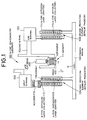
- Fig. 1 is a diagrammatic illustration showing a layout of the first embodiment of a semiconductor integrated circuit device according to the present invention. Like elements to those in Fig. 4 will be identified by same reference numerals.
- a not shown internal circuit is formed on the P-type semiconductor substrate 100. As one of elements of the internal circuit, the N-type MOSFET 111 having the N-type diffusion layer and the gate electrode is illustrated.
- the input terminal 102 and the GND terminal 103 are connected respectively.
- the GND wiring 104 connected to the GND terminal 103 one (431) of N-type diffusion layers 431 and 432 of the N-type MOSFET 111 is connected.
- the input terminal 102 is connected to the first protection element 105 via a resistor 110.
- the GND terminal 103 is directly connected to the second protection element 115.
- the input terminal 102 and the GND terminal 103 are connected to a common wiring 101 via the first and second protection elements 105 and 106.
- Respective of the first and second protection elements 105 and 106 are constructed as NPN bipolar transistors constructed with collector diffusion layers 112 and 115 and emitter diffusion layers 113 and 114.
- the collector diffusion layer 112 is connected to the input terminal 102 via the resistor 110, and the emitter diffusion layer 113 is connected to the common wiring 101.
- the collector diffusion layer 115 is directly connected to the GND terminal 103 and the emitter diffusion layer 114 is connected to the common wiring 101.
- the resistor 110 is a resistor of 5 ⁇ formed of a tungsten silicide wiring layer.
- resistance value of respective protection elements 105 and 106 in conductive state are 2 ⁇
- parasitic resistance value R of the common wiring 101 between the first and second protection elements 105 and 106 is 1 ⁇ .
- a resistance of the discharge path from the input terminal 102 to the GND terminal 103 becomes 10 ⁇ . Accordingly, when the resistor 110 is not present, the resistance becomes 5 ⁇ .
- D 100 ⁇ m
- L 100 ⁇ m
- value of approximately 30 ⁇ m is obtained as D'.
- the resistance value of the resistor 110 it is preferred to set the resistance value of the resistor 110 so that the total resistance of the discharge passage becomes less than or equal to 15 ⁇ as in the shown embodiment.
- the peak value of the discharge current is 1A
- a maximum voltage between the terminals is 15V. Since this voltage is lower than a withstanding voltage of 10 nm of silicon oxide layer, good protection of the internal circuit can be maintained.
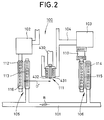
- Fig. 2 shows the second embodiment of the semiconductor integrated circuit device according to the present invention.
- the resistor 110 is disposed between the GND terminal 103 and the collector diffusion layer 115 of the second protection element 106.
- no resistor is inserted between the input terminal 102 and the first protection element 105.
- the discharge current can be limited as set out in the first embodiment, and it is possible to permit distance between the first protection element 105 and the N-type MOSFET 111 of the internal circuit.
- Fig. 3 shows the third embodiment of the semiconductor integrated circuit device according to the present invention.
- the N-type MOSFETs 111A and 111B of the internal circuit are arranged at both sides of the input terminal 102 provided on the semiconductor substrate 100.
- respective sources of these N-type MOSFETs 111A and 111B are respectively connected to first and second GND terminals 103A and 103B provided independently of each other via the GND wirings 104A and 104B.
- the input terminal 102 is connected to the collector diffusion layer 112 of the first protection element 105 via the resistor 110, and the emitter diffusion layer 113 is connected to the common wiring 101.
- respective collector diffusion layers 115A and 115B of the second protection element 106A and a third protection element 106B are connected directly.
- the emitter diffusion layers 114A and 114B of respective protection elements 106A and 106B are connected to a common wiring 101.
- the resistance of the resistor 110 is 0 ⁇ , and when the conduction resistances of respective protection elements 105A, 106A and 106B are 2 ⁇ , a parasitic resistance value R1 of the common wiring 101 from the first protection element 105 to the second protection element 106A is 1 ⁇ , and a parasitic resistance R2 of the common wiring from the first protection element 105 to the third protection element 106B is 6 ⁇ , the resistance value of the discharge passage upon application of the negative electrostatic pulse to the input terminal 102 with taking the first GND terminal 103A as reference, is 5 ⁇ , and the resistance value of the discharge passage upon application of the negative electrostatic pulse on the input terminal 102 with taking the second GND terminal 103B as reference, becomes 10 ⁇ .
- the resistor 110 is set at a resistance value greater than 0 ⁇ , for example at 5 ⁇ or so forth.
- the resistance of the discharge passage becomes 10 ⁇ if the first GND terminal 103A is selected as the reference terminal, and 15 ⁇ if the second GND terminal is selected as reference terminal.
- by providing the resistor 110 difference of the withstanding voltage and/or fluctuation due to difference of the reference terminal cab be restricted.
- the foregoing embodiments are exemplified in terms of between the input terminal and the GND terminal, the same idea is applicable even between the output terminal and the GND terminal. Also, the present invention is applicable even between the input terminal or output terminal and a power source terminal.
- the present invention can prevent the electrostatic break down voltage of internal circuit element from lowering due to discharge current which can be generated via the common wiring, by connecting resistance between the ground or power source terminal and the protection element or between the input/output terminal and the protection element. Therefore, a distance between the internal circuit element and the protection element can be reduced to require substantially no dead space to be provided so as to permit realization of higher package density or down-sizing of the chip in the LSI. Also, when a plurality of grounding terminals or the power source terminals are present, fluctuation of the withstanding voltage depending upon the terminals to be reference terminal for application of the electrostatic pulse, can be suppressed.
Landscapes
- Semiconductor Integrated Circuits (AREA)
- Bipolar Integrated Circuits (AREA)
Abstract
When an element of an internal circuit is arranged in the vicinity of an input/output terminal of an LSI chip, electrostatic break down is caused in an internal circuit element by discharge current generated between an input/output terminal and a grounding terminal or a power source terminal. Therefore, the elements are arranged with a distance to cause dead space therebetween to make down-sizing of the LSI chip difficult. Therefore, a resistor is disposed between an input/output terminal and a protection element connected thereto. The resistor causes increasing of resistance of a current path from the input/output terminal to the grounding terminal, at the common wiring. Thus influence of the electrostatic break down for the element of the internal circuit can be restricted to permit location of the resistor to permit the internal circuit element to be arranged in the vicinity of the protection element of the input/output terminal. Thus, a problem of the dead space can be solved and down-sizing of the LSI is enabled.
Description
- The present invention relates generally to a semiconductor integrated circuit device. More specifically, the invention relates to a semiconductor integrated circuit device with improved electrostatic break down voltage.
- In semiconductor integrated circuit device (hereinafter referred to as LSI), electrostatic break down voltage associating with increasing of package density becomes a problem, and various measure for protection has been taken. In general, a construction in which a diode for grounding an excessive voltage to a substrate is connected in paralle to an input/output circuit arranged between input/output terminals and an internal circuit, is employed. On the other hand, there has been proposed a construction, in which a current limiting resistor is connected in series to the input/output circuit.
- However, insertion of a electrostatic break down protection circuit constituted of the diode or resistor in such input/output circuit is not desirable for influence to input/output signals. In this point, it is considered a construction to externally connect the electrostatic break down protection circuit to the input/output circuit.
- Figs. 4 to 6 are example of the electrostatic break down protection circuit externally connected to such input/output circuit, in which Fig. 4 is a plan view, Fig. 5 is a circuit diagram of Fig. 4 and Fig. 6 is a section taken along line A - A of Fig. 4.
- In these drawings, to an
internal circuit 420 formed in a P-type semiconductor substrate 100 forming an LSI chip, aninput terminal 102 and a GND (ground)terminal 103 are connected. For respective of theinput terminal 102 and theGND terminal 103, an electrostatic break down protection circuit connected to acommon wiring 101 is connected. - Namely, to the
input terminal 102, afirst protection element 105 having an NPN bipolar transistor structure with acollector 112 and anemitter 113 of N-type diffusion layer in P-type semiconductor substrate 100, is connected. Theinput terminal 102 is connected to thecommon wiring 101 via thefirst protection element 105. Similarly, to theGND terminal 103, asecond protection element 106 having acollector 115 and anemitter 114 is connected. TheGND terminal 103 is connected to thecommon wiring 101 via thesecond protection element 106. - To the
GND wiring 104 connected to theGND terminal 103, one of N-type MOSFET 111 among N-type MOSFETs forming theinternal circuit 420 located in the vicinity of thefirst protection element 105 is arranged. - In such electrostatic break down protection circuit, with taking the
GND terminal 103 as reference, if a negative electrostatic pulse is applied to theinput terminal 102, a discharge passage is established as path Q of Fig. 5. - Namely, by applying an excessive voltage between terminals, the
first protection element 105 and thesecond protection element 106 are operated at low resistance, and an electric charge is discharged from theGND terminal 103 of Fig. 5 via thesecond protection element 106, thecommon wiring 101, thefirst protection element 105 and theinput terminal 102 to protect theinternal circuit 420. - However, in such conventional protection circuit, minority carrier injected into the
semiconductor substrate 100 by the foregoing operation of the protection element, namely electron, may damage the transistor in the vicinity of the protection element. - For example, explaining with reference to Fig. 6, when a negative electrostatic pulse is applied to the
input terminal 102 with reference to theGND terminal 103, thefirst protection circuit 105 constructed with the NPN bipolar transistor operates. Then, according to principle of operation of the bipolar transistor, the electron is injected from an N-type diffusion layer 112 connected to theinput terminal 102 to thesubstrate 100. A part of the injected electron reaches the N-type MOSFET 111 as the element to be protected and located at a distance D to be a hot electron by obtaining energy for high electrical field generated in depletion layer of junction of N-type diffusion layer 431 as source connected to theGND terminal 103. The hot electron is injected into the gate oxide layer of theMOSFET 111 to cause variation of characteristics, and to cause break down of the gate oxide layer in the worst case. - The electron injected into the
semiconductor substrate 100 from the N-type diffusion layer 112 is reduced in exponential function manner according to a distance by recombination with hole in thesemiconductor substrate 100. Namely, a density n of electron at a position distanced in D µm is substantially proportional to exp(-D/L). Here, L is a diffusion length of the electron in the P-type semiconductor substrate, and can be varied significantly depending upon fabricating condition, but in the range of approximately 100 to 500 µm. - Therefore, in the prior art, tolerance of break down is improved by setting the distance D large in the extend greater than or equal to 100 µm. However, this creates a dead space where the transistor of the internal circuit cannot be arranged, in the vicinity of the protection element. Such condition is similar with respect to the protection element of each terminal. The dead space presenting in each terminal is one of the cause preventing down-sizing of the chip.
- It is an object of the present invention to provide an LSI which can reduce a dead space, arrange protection element and element to be protected in the vicinity of each other without lowering of the electrostatic break down voltage and thus realize downsizing of the LSI chip.
- According to the first aspect of the invention, a semiconductor integrated circuit device comprises:
- an internal circuit formed on a semiconductor substrate;
- an signal terminal for supplying an input/output signal of the internal circuit;
- a power source supply terminal for supplying a power source for the internal circuit;
- a common wiring;
- a first protection element provided between the signal terminal and the common wiring for providing prevention of electrostatic break down;
- a second protection element provided between the power supply terminal and the common wiring for providing prevention of electrostatic break down; and
- a resistor element to be inserted in one of between the signal terminal and the first protection element and between the power supply terminal and the second protection element.
- The power source supply terminal to be a reference terminal, may be a grounding terminal. The power source supply terminals may be a positive or negative voltage power source terminal for supplying an operation power.
- The first protection element may be a bipolar element having a pair of first and second diffusion layers of opposite conductive type relative to the semiconductor substrate, said first and second diffusion layers are arranged in spaced apart opposition, the first diffusion layer may be connected to the signal terminal, and the second diffusion is connected to a common wiring layer. Preferably, the second protection element may be a bipolar element with a pair of third and fourth diffusion layers of the opposite conductive type, the third diffusion layer may be connected to the power source supply terminal, and the fourth diffusion layer may be connected respectively to the common wiring.
- In practice, the resistor element may be a tungsten silicide layer. A resistance of a current passage formed between the signal terminal and the power source supply terminal may be lower than or equal to 15Ω. A distance d' between the circuit element of the internal circuit and the signal terminal may satisfy

- According to another aspect of the invention, a semiconductor integrated circuit device comprises:
- an internal circuit formed on a semiconductor substrate;
- an signal terminal for supplying an input/output signal of the internal circuit;
- first and second power source supply terminals for supply power source for the internal circuit;
- a common wiring;
- a first protection element provided between the signal terminal and the common wiring for providing prevention of electrostatic break down;
- a second protection element provided between the first power supply terminal and the common wiring for providing prevention of electrostatic break down;
- a third protection element provided between the second power source supply terminal and the common wiring for providing prevention of electrostatic break down; and
- a resistor element inserted between the signal terminal and the first protection element.
- Both of the first and second power source supply terminals may be grounding terminals.
- The present invention will be understood more fully from the detailed description given herebelow and from the accompanying drawings of the preferred embodiment of the invention, which, however, should not be taken to be limitative to the present invention, but are for explanation and understanding only.
- In the drawings:
- Fig. 1 is a diagrammatic illustration showing a planar layout of the first embodiment of a semiconductor integrated circuit device according to the present invention;
- Fig. 2 is a diagrammatic illustration showing a planar layout of the second embodiment of a semiconductor integrated circuit device according to the present invention;
- Fig. 3 is a diagrammatic illustration showing a planar layout of the third embodiment of a semiconductor integrated circuit device according to the present invention;
- Fig. 4 is a diagrammatic illustration showing a planar layout of one example of conventional semiconductor integrated circuit device;
- Fig. 5 is a circuit diagram of Fig. 4; and
- Fig. 6 is a diagrammatic section taken along line A - A of Fig. 4.
- The present invention will be discussed hereinafter in detail in terms of the preferred embodiments with reference to the accompanying drawings. In the following description, numerous specific details are set forth in order to provide a thorough understanding of the present invention. It will be obvious, however, to those skilled in the art that the present invention may be practiced without these specific details. In other instance, well-known structures are not shown in detail in order to unnecessary obscure the present invention.
- Fig. 1 is a diagrammatic illustration showing a layout of the first embodiment of a semiconductor integrated circuit device according to the present invention. Like elements to those in Fig. 4 will be identified by same reference numerals. On the P-
type semiconductor substrate 100, a not shown internal circuit is formed. As one of elements of the internal circuit, the N-type MOSFET 111 having the N-type diffusion layer and the gate electrode is illustrated. - On the other hand, to the internal circuit, the
input terminal 102 and theGND terminal 103 are connected respectively. To the GND wiring 104 connected to theGND terminal 103, one (431) of N-type diffusion layers 431 and 432 of the N-type MOSFET 111 is connected. Then, theinput terminal 102 is connected to thefirst protection element 105 via aresistor 110. TheGND terminal 103 is directly connected to thesecond protection element 115. Theinput terminal 102 and theGND terminal 103 are connected to acommon wiring 101 via the first andsecond protection elements - Respective of the first and
second protection elements first protection element 105, thecollector diffusion layer 112 is connected to theinput terminal 102 via theresistor 110, and theemitter diffusion layer 113 is connected to thecommon wiring 101. - On the other hand, in the
second protection element 106, thecollector diffusion layer 115 is directly connected to theGND terminal 103 and theemitter diffusion layer 114 is connected to thecommon wiring 101. It should be noted that theresistor 110 is a resistor of 5Ω formed of a tungsten silicide wiring layer. - With the construction set forth above, when the first and
second protection elements input terminal 102 with taking theGND terminal 103 as reference, a discharge current flows through a path of theGND terminal 103, thesecond protection element 106, thecommon wiring 101, thefirst protection element 105, theresistor 110 and the input terminal to protect the internal circuit. - Here, resistance value of
respective protection elements common wiring 101 between the first andsecond protection elements input terminal 102 to theGND terminal 103 becomes 10Ω. Accordingly, when theresistor 110 is not present, the resistance becomes 5Ω. - Since a peak value of the discharge current is inversely proportional to a resistance value of the discharge path, when the
resistor 110 is present, the current is restricted to be one half of the case where theresistor 110 is not present. Therefore, at this time, the amount of electron injected from the N-type diffusion layer 112 of thefirst protection element 105 becomes substantially one half. - A condition, in which the density of electron at a position distanced at a distance D from the
first protection element 105 as theresistor 110 being not present becomes equal to the density of the electron at a distance D' as theresistor 110 being present is expressed by:
- Namely, when the
resistor 110 is not present, if break down is not caused at D = 100 µm, break down may not be caused at D' = 30 µm when theresistor 110 is present. - Furthermore, when the resistance value is increased to 10Ω, the discharge current becomes one third in comparison with the case where the
resistor 110 is not provided. At this time, similarly, a value of D' satisfying
- Namely, if break down is not caused at D = 100 µm when the
resistance 110 is not present, break down will never be caused even at zero of the distance D' when 10Ω is added asresistor 110. - In practice, when the value of the
resistor 110 is excessively large, the voltage between the terminal is elevated upon electrostatic discharge to cause degradation of protecting ability of the internal circuit. Therefore, it is preferred to set the resistance value of theresistor 110 so that the total resistance of the discharge passage becomes less than or equal to 15Ω as in the shown embodiment. In this case, when the peak value of the discharge current is 1A, a maximum voltage between the terminals is 15V. Since this voltage is lower than a withstanding voltage of 10 nm of silicon oxide layer, good protection of the internal circuit can be maintained. - Accordingly, in the shown embodiment, it becomes unnecessary to maintain unnecessarily large space between the
first protection element 105 and theelement 111 of the internal circuit, which space otherwise becomes the dead space to prevent increasing of package density of the LSI. Therefore, higher package density of the LSI or down-sizing of the chip can be achieved in the extend corresponding to the eliminated space. - Fig. 2 shows the second embodiment of the semiconductor integrated circuit device according to the present invention. In Fig. 2, like elements to those in Fig. 1 are identified by same reference numerals. In the shown embodiment, the
resistor 110 is disposed between theGND terminal 103 and thecollector diffusion layer 115 of thesecond protection element 106. On the other hand, no resistor is inserted between theinput terminal 102 and thefirst protection element 105. - Even when the
resistor 110 is connected at the side of theGND terminal 103 as set forth above, the discharge current can be limited as set out in the first embodiment, and it is possible to permit distance between thefirst protection element 105 and the N-type MOSFET 111 of the internal circuit. - Fig. 3 shows the third embodiment of the semiconductor integrated circuit device according to the present invention. In Fig. 3, like elements to those in Figs. 1 and 2 are identified by same reference numerals. In the shown embodiment, the N-
type MOSFETs input terminal 102 provided on thesemiconductor substrate 100. Also, respective sources of these N-type MOSFETs second GND terminals - The
input terminal 102 is connected to thecollector diffusion layer 112 of thefirst protection element 105 via theresistor 110, and theemitter diffusion layer 113 is connected to thecommon wiring 101. - On the other hand, to
respective GND terminals collector diffusion layers second protection element 106A and athird protection element 106B are connected directly. Theemitter diffusion layers respective protection elements common wiring 101. - In the construction set forth above, assuming that the resistance of the
resistor 110 is 0Ω, and when the conduction resistances ofrespective protection elements common wiring 101 from thefirst protection element 105 to thesecond protection element 106A is 1Ω, and a parasitic resistance R2 of the common wiring from thefirst protection element 105 to thethird protection element 106B is 6Ω, the resistance value of the discharge passage upon application of the negative electrostatic pulse to theinput terminal 102 with taking thefirst GND terminal 103A as reference, is 5Ω, and the resistance value of the discharge passage upon application of the negative electrostatic pulse on theinput terminal 102 with taking the second GND terminal 103B as reference, becomes 10Ω. - In the case where the
first GND terminal 103A is taken as reference, and a minimum distance D1 not to cause break down is assumed to be 50µm, D2 satisfying
- Namely, when the
resistor 110 is not present, a distance to the element of the internal circuit from thefirst protection element 105, at which the break down is not caused, is differentiated depending upon which of thefirst GND terminal 103A and thesecond GND terminal 103B is to be taken as reference terminal. Conversely, this means that when the distance from the protection element to the internal circuit is designed with a constant reference, the withstanding voltage can be differentiated depending upon the GND terminal selected as the reference terminal. - However, in the semiconductor integrated circuit device according to the present invention, the
resistor 110 is set at a resistance value greater than 0Ω, for example at 5Ω or so forth. In such case, the resistance of the discharge passage becomes 10Ω if thefirst GND terminal 103A is selected as the reference terminal, and 15Ω if the second GND terminal is selected as reference terminal. Then, D1' and D2' satisfying
resistor 110, difference of the withstanding voltage and/or fluctuation due to difference of the reference terminal cab be restricted. - Although the invention has been illustrated and described with respect to exemplary embodiment thereof, it should be understood by those skilled in the art that the foregoing and various other changes, omissions and additions may be made therein and thereto, without departing from the spirit and scope of the present invention. Therefore, the present invention should not be understood as limited to the specific embodiment set out above but to include all possible embodiments which can be embodies within a scope encompassed and equivalents thereof with respect to the feature set out in the appended claims.
- For instance, while the foregoing embodiments are exemplified in terms of between the input terminal and the GND terminal, the same idea is applicable even between the output terminal and the GND terminal. Also, the present invention is applicable even between the input terminal or output terminal and a power source terminal.
- As set forth above, the present invention can prevent the electrostatic break down voltage of internal circuit element from lowering due to discharge current which can be generated via the common wiring, by connecting resistance between the ground or power source terminal and the protection element or between the input/output terminal and the protection element. Therefore, a distance between the internal circuit element and the protection element can be reduced to require substantially no dead space to be provided so as to permit realization of higher package density or down-sizing of the chip in the LSI. Also, when a plurality of grounding terminals or the power source terminals are present, fluctuation of the withstanding voltage depending upon the terminals to be reference terminal for application of the electrostatic pulse, can be suppressed.
Claims (10)
- A semiconductor integrated circuit device comprising:an internal circuit formed on a semiconductor substrate;an signal terminal for supplying an input/output signal of said internal circuit;a power source supply terminal for supplying a power source for said internal circuit;a common wiring;a first protection element provided between said signal terminal and said common wiring for providing prevention of electrostatic break down;a second protection element provided between said power supply terminal and said common wiring for providing prevention of electrostatic break down; anda resistor element to be inserted in one of between the signal terminal and the first protection element and between said power supply terminal and said second protection element.
- A semiconductor integrated circuit device as set forth in claim 1, wherein said power source supply terminal to be a reference terminal, is a grounding terminal.
- A semiconductor integrated circuit device as set forth in claim 1 wherein said power source supply terminal is a positive or negative voltage power source terminal for supplying an operation power.
- A semiconductor integrated circuit device as set forth in claim 1, wherein said first protection element is a bipolar element having a pair of first and second diffusion layers of opposite conductive type relative to the semiconductor substrate, said first and second diffusion layers are arranged in spaced apart opposition, the first diffusion layer is connected to said signal terminal, and said second diffusion is connected to a common wiring layer.
- A semiconductor integrated circuit device as set forth in claim 1, wherein said second protection element is a bipolar element having a pair of third and fourth diffusion layers of opposite conductive type relative to the semiconduction substrate, said third and fourth diffusion layers are arranged in spaced apart opposition, said third diffusion layer is connected to said power source supply terminal, and said fourth diffusion layer is connected respectively to said common wiring.
- A semiconductor integrated circuit device as set forth in claim 1, wherein said resistor element is a tungsten silicide layer.
- A semiconductor integrated circuit device as set forth in claim 1, wherein a resistance of a current passage formed between said signal terminal and the power source supply terminal is lower than or equal to 15Ω.
- A semiconductor integrated circuit as set forth in claim 7, wherein a distance D' between the circuit element of said internal circuit and said signal terminal satisfies

- A semiconductor integrated circuit device comprising:an internal circuit formed on a semiconductor substrate;an signal terminal for supplying an input/output signal of said internal circuit;first and second power source supply terminals for supply power source for said internal circuit;a common wiring;a first protection element provided between said signal terminal and said common wiring for providing prevention of electrostatic break down;a second protection element provided between said first power supply terminal and said common wiring for providing prevention of electrostatic break down;a third protection element provided between said second power source supply terminal and said common wiring for providing prevention of electrostatic break down; anda resistor element inserted between the signal terminal and the first protection element.
- A semiconductor integrated circuit device as set forth in claim 9, wherein both of said first and second power source supply terminals are grounding terminals.
Applications Claiming Priority (3)
| Application Number | Priority Date | Filing Date | Title |
|---|---|---|---|
| JP29655095 | 1995-11-15 | ||
| JP7296550A JP3019760B2 (en) | 1995-11-15 | 1995-11-15 | Semiconductor integrated circuit device |
| JP296550/95 | 1995-11-15 |
Publications (2)
| Publication Number | Publication Date |
|---|---|
| EP0774784A2 true EP0774784A2 (en) | 1997-05-21 |
| EP0774784A3 EP0774784A3 (en) | 2000-07-19 |
Family
ID=17834993
Family Applications (1)
| Application Number | Title | Priority Date | Filing Date |
|---|---|---|---|
| EP96118277A Withdrawn EP0774784A3 (en) | 1995-11-15 | 1996-11-14 | Semiconductor integrated circuit device including protection means |
Country Status (5)
| Country | Link |
|---|---|
| US (1) | US5828107A (en) |
| EP (1) | EP0774784A3 (en) |
| JP (1) | JP3019760B2 (en) |
| KR (1) | KR100206675B1 (en) |
| TW (1) | TW314656B (en) |
Cited By (1)
| Publication number | Priority date | Publication date | Assignee | Title |
|---|---|---|---|---|
| DE19721322A1 (en) * | 1996-11-19 | 1998-05-20 | Lg Semicon Co Ltd | Protective circuit against electrostatic discharge |
Families Citing this family (8)
| Publication number | Priority date | Publication date | Assignee | Title |
|---|---|---|---|---|
| JP2954153B1 (en) | 1998-04-07 | 1999-09-27 | 日本電気アイシーマイコンシステム株式会社 | Semiconductor integrated circuit |
| KR100506970B1 (en) * | 1998-09-01 | 2005-10-26 | 삼성전자주식회사 | Electrostatic Discharge Prevention Semiconductor Device |
| US6268286B1 (en) | 2000-02-01 | 2001-07-31 | International Business Machines Corporation | Method of fabricating MOSFET with lateral resistor with ballasting |
| US6700164B1 (en) | 2000-07-07 | 2004-03-02 | International Business Machines Corporation | Tungsten hot wire current limiter for ESD protection |
| CN1244152C (en) | 2001-11-16 | 2006-03-01 | 松下电器产业株式会社 | Semiconductor device |
| US8363365B2 (en) * | 2008-06-17 | 2013-01-29 | Semiconductor Energy Laboratory Co., Ltd. | Semiconductor device |
| JP5595751B2 (en) * | 2009-03-11 | 2014-09-24 | ルネサスエレクトロニクス株式会社 | ESD protection element |
| JP2014225483A (en) * | 2011-09-16 | 2014-12-04 | パナソニック株式会社 | Semiconductor integrated circuit device |
Family Cites Families (8)
| Publication number | Priority date | Publication date | Assignee | Title |
|---|---|---|---|---|
| NL176322C (en) * | 1976-02-24 | 1985-03-18 | Philips Nv | SEMICONDUCTOR DEVICE WITH SAFETY CIRCUIT. |
| JPH061833B2 (en) * | 1982-11-11 | 1994-01-05 | 株式会社東芝 | MOS semiconductor device |
| JPS6010765A (en) * | 1983-06-30 | 1985-01-19 | Fujitsu Ltd | Semiconductor device |
| JP3318774B2 (en) * | 1992-06-29 | 2002-08-26 | ソニー株式会社 | Semiconductor device and solid-state imaging device |
| JP2958202B2 (en) * | 1992-12-01 | 1999-10-06 | シャープ株式会社 | Semiconductor device |
| JP2972494B2 (en) * | 1993-06-30 | 1999-11-08 | 日本電気株式会社 | Semiconductor device |
| US5616943A (en) * | 1993-09-29 | 1997-04-01 | At&T Global Information Solutions Company | Electrostatic discharge protection system for mixed voltage application specific integrated circuit design |
| JP2638462B2 (en) * | 1993-12-29 | 1997-08-06 | 日本電気株式会社 | Semiconductor device |
-
1995
- 1995-11-15 JP JP7296550A patent/JP3019760B2/en not_active Expired - Lifetime
-
1996
- 1996-11-08 US US08/748,495 patent/US5828107A/en not_active Expired - Lifetime
- 1996-11-14 KR KR1019960053909A patent/KR100206675B1/en not_active Expired - Fee Related
- 1996-11-14 TW TW085113942A patent/TW314656B/zh not_active IP Right Cessation
- 1996-11-14 EP EP96118277A patent/EP0774784A3/en not_active Withdrawn
Non-Patent Citations (1)
| Title |
|---|
| None |
Cited By (2)
| Publication number | Priority date | Publication date | Assignee | Title |
|---|---|---|---|---|
| DE19721322A1 (en) * | 1996-11-19 | 1998-05-20 | Lg Semicon Co Ltd | Protective circuit against electrostatic discharge |
| DE19721322B4 (en) * | 1996-11-19 | 2007-08-16 | LG Semicon Co., Ltd., Cheongju | Electrostatic discharge protection device |
Also Published As
| Publication number | Publication date |
|---|---|
| JPH09139468A (en) | 1997-05-27 |
| KR100206675B1 (en) | 1999-07-01 |
| TW314656B (en) | 1997-09-01 |
| EP0774784A3 (en) | 2000-07-19 |
| KR970030780A (en) | 1997-06-26 |
| JP3019760B2 (en) | 2000-03-13 |
| US5828107A (en) | 1998-10-27 |
Similar Documents
| Publication | Publication Date | Title |
|---|---|---|
| US5717559A (en) | Input/output protection device for use in semiconductor device | |
| JP2638462B2 (en) | Semiconductor device | |
| JP3485655B2 (en) | Composite MOSFET | |
| JP2810874B2 (en) | Semiconductor device | |
| US4811155A (en) | Protection circuit for a semiconductor integrated circuit having bipolar transistors | |
| US6222710B1 (en) | Semiconductor device | |
| US5786616A (en) | Semiconductor integrated circuit having an SOI structure, provided with a protective circuit | |
| JPS6358380B2 (en) | ||
| JP2007235151A (en) | Protection structure for integrated circuits | |
| EP0315213A2 (en) | Vertical mosfet device having protector | |
| US4656491A (en) | Protection circuit utilizing distributed transistors and resistors | |
| KR19980064705A (en) | Semiconductor devices | |
| US5684323A (en) | Protection circuit for semiconductor device | |
| EP0253105B1 (en) | Integrated circuit with improved protective device | |
| US5019883A (en) | Input protective apparatus of semiconductor device | |
| EP0774784A2 (en) | Semiconductor integrated circuit device including protection means | |
| US5909046A (en) | Semiconductor integrated circuit device having stable input protection circuit | |
| US4990984A (en) | Semiconductor device having protective element | |
| JP2906749B2 (en) | Gate protection device for semiconductor device | |
| US6163056A (en) | Semiconductor device having electrostatic discharge | |
| EP0198468B1 (en) | Protective device for integrated circuit | |
| JPH0821630B2 (en) | Semiconductor device | |
| US5929491A (en) | Integrated circuit with ESD protection | |
| JPH0373574A (en) | Semiconductor integrated circuit | |
| JP3206703B2 (en) | Semiconductor device |
Legal Events
| Date | Code | Title | Description |
|---|---|---|---|
| PUAI | Public reference made under article 153(3) epc to a published international application that has entered the european phase |
Free format text: ORIGINAL CODE: 0009012 |
|
| AK | Designated contracting states |
Kind code of ref document: A2 Designated state(s): DE FR GB |
|
| PUAL | Search report despatched |
Free format text: ORIGINAL CODE: 0009013 |
|
| AK | Designated contracting states |
Kind code of ref document: A3 Designated state(s): DE FR GB |
|
| 17P | Request for examination filed |
Effective date: 20000616 |
|
| 17Q | First examination report despatched |
Effective date: 20001004 |
|
| STAA | Information on the status of an ep patent application or granted ep patent |
Free format text: STATUS: THE APPLICATION HAS BEEN WITHDRAWN |
|
| 18W | Application withdrawn |
Withdrawal date: 20010410 |