EP0773149A2 - Fahrzeug -Sicherheitssystem - Google Patents
Fahrzeug -Sicherheitssystem Download PDFInfo
- Publication number
- EP0773149A2 EP0773149A2 EP96402360A EP96402360A EP0773149A2 EP 0773149 A2 EP0773149 A2 EP 0773149A2 EP 96402360 A EP96402360 A EP 96402360A EP 96402360 A EP96402360 A EP 96402360A EP 0773149 A2 EP0773149 A2 EP 0773149A2
- Authority
- EP
- European Patent Office
- Prior art keywords
- piezoelectric disk
- input
- alarm system
- vehicle
- weight
- Prior art date
- Legal status (The legal status is an assumption and is not a legal conclusion. Google has not performed a legal analysis and makes no representation as to the accuracy of the status listed.)
- Granted
Links
- 230000035939 shock Effects 0.000 claims abstract description 67
- 239000003990 capacitor Substances 0.000 claims description 29
- 239000000758 substrate Substances 0.000 claims description 12
- 230000001960 triggered effect Effects 0.000 abstract description 17
- 230000035945 sensitivity Effects 0.000 description 9
- 230000008859 change Effects 0.000 description 6
- 230000008901 benefit Effects 0.000 description 4
- 230000006870 function Effects 0.000 description 4
- 238000009434 installation Methods 0.000 description 4
- 238000005452 bending Methods 0.000 description 3
- 238000001514 detection method Methods 0.000 description 3
- 238000005476 soldering Methods 0.000 description 3
- 230000009286 beneficial effect Effects 0.000 description 2
- 230000033001 locomotion Effects 0.000 description 2
- 238000000034 method Methods 0.000 description 2
- 230000009471 action Effects 0.000 description 1
- 230000003321 amplification Effects 0.000 description 1
- 238000013459 approach Methods 0.000 description 1
- 230000005540 biological transmission Effects 0.000 description 1
- 239000000919 ceramic Substances 0.000 description 1
- 238000006243 chemical reaction Methods 0.000 description 1
- 230000001143 conditioned effect Effects 0.000 description 1
- 238000007796 conventional method Methods 0.000 description 1
- 239000013078 crystal Substances 0.000 description 1
- 238000013016 damping Methods 0.000 description 1
- 230000003247 decreasing effect Effects 0.000 description 1
- 238000013461 design Methods 0.000 description 1
- 230000009977 dual effect Effects 0.000 description 1
- 230000007613 environmental effect Effects 0.000 description 1
- 238000011156 evaluation Methods 0.000 description 1
- 230000015654 memory Effects 0.000 description 1
- 238000012986 modification Methods 0.000 description 1
- 230000004048 modification Effects 0.000 description 1
- 238000012544 monitoring process Methods 0.000 description 1
- 238000003199 nucleic acid amplification method Methods 0.000 description 1
- 230000010355 oscillation Effects 0.000 description 1
- 239000000779 smoke Substances 0.000 description 1
- 239000007787 solid Substances 0.000 description 1
- 238000012358 sourcing Methods 0.000 description 1
- 238000012546 transfer Methods 0.000 description 1
Images
Classifications
-
- B—PERFORMING OPERATIONS; TRANSPORTING
- B60—VEHICLES IN GENERAL
- B60R—VEHICLES, VEHICLE FITTINGS, OR VEHICLE PARTS, NOT OTHERWISE PROVIDED FOR
- B60R25/00—Fittings or systems for preventing or indicating unauthorised use or theft of vehicles
- B60R25/10—Fittings or systems for preventing or indicating unauthorised use or theft of vehicles actuating a signalling device
- B60R25/1001—Alarm systems associated with another car fitting or mechanism, e.g. door lock or knob, pedals
-
- G—PHYSICS
- G01—MEASURING; TESTING
- G01P—MEASURING LINEAR OR ANGULAR SPEED, ACCELERATION, DECELERATION, OR SHOCK; INDICATING PRESENCE, ABSENCE, OR DIRECTION, OF MOVEMENT
- G01P15/00—Measuring acceleration; Measuring deceleration; Measuring shock, i.e. sudden change of acceleration
- G01P15/02—Measuring acceleration; Measuring deceleration; Measuring shock, i.e. sudden change of acceleration by making use of inertia forces using solid seismic masses
- G01P15/08—Measuring acceleration; Measuring deceleration; Measuring shock, i.e. sudden change of acceleration by making use of inertia forces using solid seismic masses with conversion into electric or magnetic values
- G01P15/09—Measuring acceleration; Measuring deceleration; Measuring shock, i.e. sudden change of acceleration by making use of inertia forces using solid seismic masses with conversion into electric or magnetic values by piezoelectric pick-up
- G01P15/0922—Measuring acceleration; Measuring deceleration; Measuring shock, i.e. sudden change of acceleration by making use of inertia forces using solid seismic masses with conversion into electric or magnetic values by piezoelectric pick-up of the bending or flexing mode type
Definitions
- the present invention is directed to an improved input unit for a vehicle security system, such as a vehicle alarm system, which can accept either positively or negatively triggered inputs.
- a vehicle security system such as a vehicle alarm system
- the present invention also relates to a sensor system which can be utilized in a vehicle security system.
- Vehicle alarm systems also commonly use a piezoelectric disk as a shock sensor.
- These devices are man-made electro-mechanical devices that are used in many common household devices, in addition to use in vehicle alarm systems. Such devices are used as buzzer alarms in smoke detectors, ringers in telephones, sounders in pagers, etc.
- Such piezoelectric disks are very efficient in converting electrical energy into sound (mechanical) energy. As in all such crystalline devices, such an energy conversion also works in reverse. That is, applying an electrical impulse across a piezoelectric disk causes the piezoelectric disk to bend. Conversely, applying a bending moment to the piezoelectric disk generates an electrical impulse across the piezoelectric disk, which can then be sensed. This sensing operation is used in implementing a piezoelectric disk as a shock sensor by sensing the electrical impulse generated when the piezoelectric disk is bent.
- the mass of a typical piezoelectric disk which is for example 25 mm in diameter, is very low. As a result, an impulse of motion (e.g., a shock) applied to the piezoelectric disk is not easily detected. As a result, a significantly larger mass must be applied to the piezoelectric disk for the piezoelectric disk to detect a shock. This is often accomplished, and with reference to Figure 1, as expediently as soldering a weight 30, such as a bolt, to piezoelectric disk 20. By rigidly fastening one edge 40 of the piezoelectric disk 20, e.g.
- the piezoelectric disk 20 will oscillate in a damping fashion with a moment arm equal to the distance from a center of mass 60 to the rigidly mounted edge 40 of the piezoelectric disk 20. Due to the very high ratio of the mass of the weight 30 to the mass of the piezoelectric disk 20, the center of mass of the system is nominally the same as the center of mass 60 of the weight 30, which is attached at the mounting 50 to the piezoelectric disk 20.
- This mounting 50 may typically also be a soldering.
- Figure 1 shows a typical shock sensor as conventionally used in many vehicle alarm systems.
- the weight 30 is conventionally soldered to the piezoelectric disk 20 at point 50 between the center and far top of the piezoelectric disk 20 to get as great a moment arm as possible.
- the fastened edge 40 of the piezoelectric disk 20 to the substrate 10 provides one side of the electrical output and a wire (not shown in Figure 1) soldered to a ceramic crystal surface of the piezoelectric disk 20 provides another output.
- a movement of the weight 30 causes a bending in the piezoelectric disk 20, which generates an electrical signal which is often several volts in amplitude and which alternates at a frequency which is equal to a mechanical resonance of the system. Typical resonances are from hundreds of cycles per second to several thousand cycles per second.
- a conventional alarm system utilizes a peak voltage detector on the output of the electrical signal from the sensor shown in Figure 1. When the amplitude of the output signal exceeds a predetermined threshold level, an alarm situation is detected and an alarm is activated. Sensitivity of the system can be adjusted by varying the threshold level detected.
- a conventional shock detector circuit is shown in Figure 2 of the present specification.
- the signals received from the piezoelectric sensor 20 are input into an operational amplifier 22.
- the signal output by amplifier 22 is then fed into a comparator 27 through a diode 23.
- the other input into comparator 27 is fed from potentiometer R26. Based on adjusting potentiometer 26, the threshold level can be adjusted.
- a conventional shock detector circuit as shown in Figure 2, when the signal input from piezoelectric disk 20 exceeds the level set by threshold adjuster R26, a shock is detected and a signal indicating such is output to an alarm system.
- one object of the present invention is to provide a novel input circuitry for a vehicle alarm system which can accept inputs from both a negatively triggered pin switch and a positively triggered pin switch.
- One further object of the system of the present invention is to provide a novel shock sensor which provides an enhanced operation of detecting shocks.
- the present invention achieves its objectives by providing a novel input circuitry which can receive inputs from both negatively triggered and positively triggered pin switches.
- the present invention also achieves its objectives by a novel technique of mounting a mass onto a piezoelectric disk, and a novel technique of then sensing signals generated by this piezoelectric disk structure. More specifically, in this feature of the present invention, a mass which is attached to the piezoelectric disk is mounted off of a central axis of the piezoelectric disk. The sensing operation also takes advantage of all information from the signal output by the piezoelectric disk sensor.
- the system of the present invention requires only one input which can receive both negatively triggered and positively triggered pin switches. This provides a significant advantage over the conventional systems which utilize two inputs, as the system of the present invention does not require any redundant circuitry. Furthermore, the system of the present invention provides a significant advantage of simplifying installation as only one input is needed.
- the circuitry of the present invention specifically operates to accept either positively triggered or negatively triggered pin switches at the input.
- the system of the present invention has connected to the input a resistor R1, which in turn is also connected to a battery of a vehicle, which may be between +12-14 V. Also connected to the input is a resistor R2 which is also connected to ground. The values of each of these resistors R1 and R2 may be 1 K ⁇ , as examples only.
- the input is also connected to a point between two capacitors C1 and C2, which in turn are respectively connected to a +5 V biased output and a ground biased output through respective resistors R5 and R6.
- Connected to a point between capacitor C1 and resistor R5 is a further resistor R3, which is also connected to a +5 V source.
- Connected to a point between capacitor C2 and resistor R6 is a further resistor R4, which is also connected to ground.
- the circuit shown in Figure 3 provides a beneficial operation of eliminating a need for two wires that perform the same function, and eliminating a need of identifying a polarity of a vehicle door pin switch.
- the circuit shown in Figure 3 essentially accomplishes a DC isolated input-output system which only passes an AC pulse to dual outputs.
- the input is biased to 6-7 V DC through a voltage divider formed of resistors R1 and R2. This bias is generally maintained when the door is closed since a dome lamp side of the door pin switch is generally an open circuit in this state.
- a solid 6 or 7 V input pulse appears at the input as the door pin switch provides a path to +12 V or ground.
- Such a pulse is passed through the two different capacitors C1 and C2, capacitor C2 has an output side biased at ground through resistor R4, which may be a 1 M ⁇ resistor as an example only, and capacitor C1 has an output side biased at +5 V through resistor R3, which may also be a 1 M ⁇ resistor as an example only.
- the pulses are passed through resistors R5 and R6 to a diode protected current sourcing/sinking input of a conventional microprocessor 35, whose voltage supply is 5 V.
- a conventional microprocessor 35 whose voltage supply is 5 V.
- a negative pulse on the ground biased output side through resistor R6 causes the microprocessor 35 to source 0.2 mA, but this does not produce a voltage change on the output because of the diode protected input of the microprocessor 35.
- This same pulse causes a -6 or -7 V pulse on the +5 output side through resistor R5 and produces a voltage change of -5 V at the microprocessor 35.
- This voltage change of -5 V on the microprocessor 35 thus allows the microprocessor 35 to detect the negative pulse.
- the microprocessor 35 can look for a door closing after some simple set-up condition and use that pulse to know when the door is closed, and the opposite pulse to know when the door is opened. As a result, the microprocessor 35 will then only enter into an alarm mode when the vehicle door is opened.
- FIG. 4 of the present specification shows the improved weight mounting system of the present invention.
- a piezoelectric sensor should be designed to handle all variations in its mounting position, and to permit such a system to be arbitrarily installed, and to provide consistent results in any type of environment.
- an ideal piezoelectric sensor should work identically regardless of a direction from which a shock originates.
- the piezoelectric sensor must be orthogonally independent.
- orthogonal coordinates are shown with directions X, Y and Z labeled.
- any shock applied in the Z direction is applied in an angular moment arm of approximately 2R, where R is the radius of the piezoelectric disk 20.
- the system then vibrates with the center of mass acting on the approximate distance 4R 2 + A 2 (representing the distance from the rigid mounting 40 to the center of mass 60) and flexing the piezoelectric disk 20 across its center, thereby generating a large electrical signal.
- the angular moment arm is only the distance A long (representing the distance from mounting 50 to the center of mass 60).
- the piezoelectric disk 20 cannot bend since it is "on end" by virtue of its rigid attachment to substrate 10 at point 40, and therefore with such a shock along the Y axis, the piezoelectric disk 20 can only generate a torsional twist around the X axis (shown by the arrow at the X axis). This results in generating an electrical signal from a shock along the Y axis which is very different from the bending signal of a shock along the Z axis. Both the frequency and the amplitude of the electrical signals generated by these two different shocks are very different.
- Table 1 Shown below in Table 1 is a chart which summarizes the operating nature of the conventional system shown in Figure 1.
- TABLE 1 DIRECTION OF SHOCK APPLIED ANGULAR MOMENT ARM VIBRATION ARM RELATIVE SIGNAL STRENGTH X A 4R 2 + A 2 Largest Y A Torsional Small Z 2R 4R 2 + A 2 Large
- the mounting position of the weight 30 differs in the system of the present invention from that in the conventional system shown in Figure 1. More specifically, this weight 30 is mounted in a position which approximates the radius R away (e.g. 0.8R) from the center of the piezoelectric disk 20, and at a position halfway up the piezoelectric disk 20 and out to one edge of the piezoelectric disk 20, i.e. on a diameter of the piezoelectric disk 20 which is parallel to the substrate 10.
- R away e.g. 0.8R
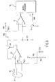
- the circuit shown in Figure 6 is an enhanced circuit for reading the signals generated by the piezoelectric circuit of Figure 4.
- the conventional shock detector circuit shown in Figure 2 operates as a voltage amplification and peak detection circuit which determines when to set off an alarm.
- the system shown in Figure 6 has two functions, a first function is detection of an overall energy in a given shock, and another function is establishing a compensating detection threshold for an alarm.
- a size (voltage) of a largest peak signal is not a complete description of the type or size of the shock signal.
- a signal detected by a piezoelectric sensor is a signal which has been heavily filtered by the transmission medium (e.g., the vehicle, the frame, etc.) as well as being affected by the source (e.g., a hammer, a kick, a crowbar, etc.).
- the shock detector circuit shown in Figure 6 integrates an entire shock signal to measure the entire energy in the shock signal.
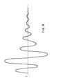
- the signal generated by a piezoelectric disk 20 is a damped sine wave which lasts several hundred milliseconds over many cycles, as is shown for example in Figure 5.
- the circuitry shown in Figure 6 is used to integrate the entire area under one-half of the signal shown in Figure 5, to thus evaluate a full significance of the received shock signal.
- the circuit shown in Figure 6 integrates all of the positive half of the oscillations from the signal output from piezoelectric disk 20 and accumulates them as a voltage across a capacitor C72.
- the circuit shown in Figure 6 operates as follows.
- An input signal from the piezoelectric disk 20 is input to an operational amplifier 65 across a resistor R61, which may have a value of 100 K ⁇ , as an example only.
- an electrical signal from the piezoelectric disk 20 is generated across resistor R61.
- One side of this signal is a reference voltage which is applied to a positive terminal of the operational amplifier 65, which may typically be an LM3324, or such.
- the negative input to this operational amplifier 65 is connected to the other side of resistor R61, which is represented as V REF1 , which is the "node" of virtual ground of the operation amplifier 65.
- resistors R62 and R63 are Also connected to the node V REF1 in parallel.
- Resistor R62 is also connected to the +V source and resistor R63 is also connected to ground.
- a capacitor C70 is connected to a point between resistor R62 and R63 and ground.
- Resistors R62, R63 and capicitor C70 provide a voltage divider network for voltage V REF1 .
- Amplifier 65 also has a feedback loop through a base emitter junction of a PNP transistor 68. As a result, when the input from the piezoelectric disk 20 goes positive, the feedback is a forward diode junction, and when the input from the piezoelectric disk 20 goes negative, the feedback is a reverse bias diode junction (high impedance).
- the emitter current of transistor 68 on the positive input signals is reflected in the collector of transistor 68 which charges capacitor C72, which is connected to the emitter of transistor 68.
- the total current is scaled by the value of resistor R61, and the total current is an integrated area of the positive signals generated by piezoelectric disk 20, and as is represented by the shaded area in Figure 5.
- a positive input of a second operational amplifier 70 is also connected to this emitter current.
- a negative input to this operational amplifier 70 receives a reference voltage V REF2 through a reference voltage source +V and a voltage divider formed of resistors R64 and R65, which may take on the respective values of 22 K ⁇ and 4.7 K ⁇ , as examples only.
- This voltage +V may typically be 12 V.
- microprocessor 75 This fact of this positive output of amplifier 70 is stored in an accumulator register in microprocessor 75.
- the microprocessor 75 then also cleans up or "dumps" the charge on capacitor C72. More specifically, an output from microprocessor 75 is fed through a resistor R66 and a transistor 74 to the positive input of amplifier 70, resistor R66 may have a value of 2.2 K ⁇ as an example only.
- Microprocessor 75 puts a short pulse on resistor R66, which causes transistor 74 to turn on for a short period of time, to thereby remove (or "dump") the charge on capacitor C72.
- each "dump" of capacitor C72 represents a scaled portion of a shock pulse. In the absence of actual shock pulses, there is also a normal vibration which is being sensed. In addition, various leakage currents would cause capacitor C72 to charge up at an arbitrary, but continuous, rate. Thus, there is a zero based rate of dump cycles.
- a typical system may have an operation to dump capacitor C72 five times per second. The microprocessor 75 may use such information to calculate a zero baseline for measuring shock.
- the time between "dumps" may decrease to several milliseconds at the area of peak voltage.
- the energy of a shock is therefore measured by the difference between the baseline dumps and the actual dumps measured over any period of time.
- Microprocessor 75 initiates the "dumps" based on a value in the accumulator therein. Since each shock results in energy received over several hundred milliseconds, a typical convenient period of time to evaluate the shock energy received may be a quarter of a second.
- a second measure of the strength of a shock is the time between dumps. This measures the peak energy of a shock.
- the microprocessor 75 also features a register to store data as to the time between dumps.
- the system of the present invention makes use of both the peak energy and the average energy to decide an alarm condition, as described below.
- the system of the present invention overcomes such shortcomings in the conventional systems by more accurately determining a shock condition utilizing all information available.
- the present invention utilizes a first criteria to issue an alarm condition if the energy level of the shock is high enough to result in two dumps of the voltage in capacitor C72 within a predetermined period of time (T). This determination can be further conditioned on if a certain number of further dumps (X) of the voltage in capacitor C72 result within a predetermined period of time, for example 250 milliseconds, following the first two dumps.
- the system of the present invention may be operated so that if two dumps ever occur 2.5 milliseconds apart or less, and further if there are more than 16 dumps in a subsequent 250 milliseconds, it is determined by microprocessor 75 that an alarm condition is to be indicated.
- the system of the present invention may have a further independent evaluation by microprocessor 75 which simply evaluates whether a certain number of dumps (Y) occurs over any continuous 250 millisecond period.
- the system of the present invention may determine whether, for example, 32 dumps occur during any continuous 250 millisecond time period, which would then result in an alarm condition being issued.
- system of the present invention can adjust the specific values and such values could also be updated continuously based on different environmental conditions.
- the sensitivity of an alarm can be adjusted by an installer, and perhaps later by the user of the alarm system. Such an operation may be necessary because each vehicle is different and each mounting is different, and each component in the system would have different characteristics, such as piezo gain.
- a typical sensitivity selecting sequence would operate as follows. To set the shock level, one button on the transmitter can be pushed and held and the second button can be quickly pushed a predetermined number of times. Both buttons can then be released as the vehicle headlights light up to quickly flash 1 to 8 times. This flashing of the headlights would indicate the current shock sensitivity level, for example the higher the number of flashes the more sensitive the setting. Then, one of the buttons on the transmitter can be pushed a predetermined number of times, and each time the button is pushed the sensitivity level can be either increased or decreased by 1. Obviously, other operations of changing the sensitivity could also be implemented.
Landscapes
- Physics & Mathematics (AREA)
- General Physics & Mathematics (AREA)
- Engineering & Computer Science (AREA)
- Mechanical Engineering (AREA)
- Burglar Alarm Systems (AREA)
- Emergency Alarm Devices (AREA)
Applications Claiming Priority (2)
| Application Number | Priority Date | Filing Date | Title |
|---|---|---|---|
| US08/555,285 US5783988A (en) | 1995-11-08 | 1995-11-08 | Vehicle security system |
| US555285 | 1995-11-08 |
Publications (3)
| Publication Number | Publication Date |
|---|---|
| EP0773149A2 true EP0773149A2 (de) | 1997-05-14 |
| EP0773149A3 EP0773149A3 (de) | 1998-04-22 |
| EP0773149B1 EP0773149B1 (de) | 2003-06-18 |
Family
ID=24216693
Family Applications (1)
| Application Number | Title | Priority Date | Filing Date |
|---|---|---|---|
| EP96402360A Expired - Lifetime EP0773149B1 (de) | 1995-11-08 | 1996-11-06 | Fahrzeug -Sicherheitssystem |
Country Status (5)
| Country | Link |
|---|---|
| US (1) | US5783988A (de) |
| EP (1) | EP0773149B1 (de) |
| AT (1) | ATE243125T1 (de) |
| CA (1) | CA2189821C (de) |
| DE (1) | DE69628716D1 (de) |
Family Cites Families (5)
| Publication number | Priority date | Publication date | Assignee | Title |
|---|---|---|---|---|
| US3794967A (en) * | 1972-08-03 | 1974-02-26 | L Fischer | Intruder alarm for automobiles |
| US3815088A (en) * | 1972-12-04 | 1974-06-04 | Sheldon Aircraft Prod Corp | Vehicle alarm circuit responsive to selected battery voltage transients |
| US4383242A (en) * | 1979-06-04 | 1983-05-10 | Tmx Systems Limited | Automobile anti-theft system |
| US4887064A (en) * | 1987-12-28 | 1989-12-12 | Clifford Electronics, Inc. | Multi-featured security system with self-diagnostic capability |
| JPH04102029U (ja) * | 1991-02-13 | 1992-09-03 | ユピテル工業株式会社 | 振動センサ |
-
1995
- 1995-11-08 US US08/555,285 patent/US5783988A/en not_active Expired - Lifetime
-
1996
- 1996-11-06 EP EP96402360A patent/EP0773149B1/de not_active Expired - Lifetime
- 1996-11-06 AT AT96402360T patent/ATE243125T1/de not_active IP Right Cessation
- 1996-11-06 DE DE69628716T patent/DE69628716D1/de not_active Expired - Lifetime
- 1996-11-07 CA CA002189821A patent/CA2189821C/en not_active Expired - Lifetime
Non-Patent Citations (1)
| Title |
|---|
| None |
Also Published As
| Publication number | Publication date |
|---|---|
| DE69628716D1 (de) | 2003-07-24 |
| CA2189821A1 (en) | 1997-05-09 |
| CA2189821C (en) | 2003-02-11 |
| EP0773149B1 (de) | 2003-06-18 |
| ATE243125T1 (de) | 2003-07-15 |
| EP0773149A3 (de) | 1998-04-22 |
| US5783988A (en) | 1998-07-21 |
Similar Documents
| Publication | Publication Date | Title |
|---|---|---|
| US7098675B2 (en) | Capacitance change detection device | |
| CN100371735C (zh) | 超声传感器 | |
| US5008647A (en) | Wireless bicycle wheel monitor system | |
| US7015824B2 (en) | Trailer cargo detection using ultrasonic transducers | |
| US4122437A (en) | Intrusion alarm control system | |
| US7290437B1 (en) | Sensor node for impact detection | |
| CN100381967C (zh) | 信号测量电路 | |
| US4125826A (en) | Ultrasonic vehicle alarm system | |
| US4057791A (en) | Motion responsive alarm system | |
| US4450437A (en) | Motion alarm system | |
| US4651128A (en) | Method of monitoring the inclination of a motor vehicle | |
| US8229664B2 (en) | Curb detection device for motor vehicles | |
| US6265676B1 (en) | Systems and processing algorithms for ultrasound time-of-flight digitizer systems | |
| US5376925A (en) | Motion and direction sensors | |
| US5107249A (en) | Intrusion detection system having improved immunity to false alarm | |
| US5159837A (en) | Ultrasonic wave obstacle sensor | |
| CA2134541C (en) | Infrared detection switching circuit | |
| EP1113260B1 (de) | Objektsensor und seine Anwendung in einer Scheibenwischersteuerungsschaltung | |
| WO1989002635A1 (en) | Proximity sensor | |
| EP0773149B1 (de) | Fahrzeug -Sicherheitssystem | |
| WO1993019385A1 (en) | A device for and method of surveillance of a space | |
| US4380807A (en) | Echo recognition system | |
| US4667195A (en) | Rear monitor system triggered by occupant leaving the vehicle | |
| CA1154140A (en) | Echo recognition system | |
| US5912620A (en) | Combined type intrusion and attack sensing means |
Legal Events
| Date | Code | Title | Description |
|---|---|---|---|
| PUAI | Public reference made under article 153(3) epc to a published international application that has entered the european phase |
Free format text: ORIGINAL CODE: 0009012 |
|
| AK | Designated contracting states |
Kind code of ref document: A2 Designated state(s): AT BE CH DE DK ES FI FR GB GR IE IT LI LU MC NL PT SE |
|
| PUAL | Search report despatched |
Free format text: ORIGINAL CODE: 0009013 |
|
| AK | Designated contracting states |
Kind code of ref document: A3 Designated state(s): AT BE CH DE DK ES FI FR GB GR IE IT LI LU MC NL PT SE |
|
| 17P | Request for examination filed |
Effective date: 19981009 |
|
| 17Q | First examination report despatched |
Effective date: 20020517 |
|
| GRAH | Despatch of communication of intention to grant a patent |
Free format text: ORIGINAL CODE: EPIDOS IGRA |
|
| GRAH | Despatch of communication of intention to grant a patent |
Free format text: ORIGINAL CODE: EPIDOS IGRA |
|
| GRAA | (expected) grant |
Free format text: ORIGINAL CODE: 0009210 |
|
| AK | Designated contracting states |
Designated state(s): AT BE CH DE DK ES FI FR GB GR IE IT LI LU MC NL PT SE |
|
| PG25 | Lapsed in a contracting state [announced via postgrant information from national office to epo] |
Ref country code: NL Free format text: LAPSE BECAUSE OF FAILURE TO SUBMIT A TRANSLATION OF THE DESCRIPTION OR TO PAY THE FEE WITHIN THE PRESCRIBED TIME-LIMIT Effective date: 20030618 Ref country code: LI Free format text: LAPSE BECAUSE OF FAILURE TO SUBMIT A TRANSLATION OF THE DESCRIPTION OR TO PAY THE FEE WITHIN THE PRESCRIBED TIME-LIMIT Effective date: 20030618 Ref country code: IT Free format text: LAPSE BECAUSE OF FAILURE TO SUBMIT A TRANSLATION OF THE DESCRIPTION OR TO PAY THE FEE WITHIN THE PRESCRIBED TIME-LIMIT;WARNING: LAPSES OF ITALIAN PATENTS WITH EFFECTIVE DATE BEFORE 2007 MAY HAVE OCCURRED AT ANY TIME BEFORE 2007. THE CORRECT EFFECTIVE DATE MAY BE DIFFERENT FROM THE ONE RECORDED. Effective date: 20030618 Ref country code: FR Free format text: LAPSE BECAUSE OF FAILURE TO SUBMIT A TRANSLATION OF THE DESCRIPTION OR TO PAY THE FEE WITHIN THE PRESCRIBED TIME-LIMIT Effective date: 20030618 Ref country code: FI Free format text: LAPSE BECAUSE OF FAILURE TO SUBMIT A TRANSLATION OF THE DESCRIPTION OR TO PAY THE FEE WITHIN THE PRESCRIBED TIME-LIMIT Effective date: 20030618 Ref country code: CH Free format text: LAPSE BECAUSE OF FAILURE TO SUBMIT A TRANSLATION OF THE DESCRIPTION OR TO PAY THE FEE WITHIN THE PRESCRIBED TIME-LIMIT Effective date: 20030618 Ref country code: BE Free format text: LAPSE BECAUSE OF FAILURE TO SUBMIT A TRANSLATION OF THE DESCRIPTION OR TO PAY THE FEE WITHIN THE PRESCRIBED TIME-LIMIT Effective date: 20030618 Ref country code: AT Free format text: LAPSE BECAUSE OF FAILURE TO SUBMIT A TRANSLATION OF THE DESCRIPTION OR TO PAY THE FEE WITHIN THE PRESCRIBED TIME-LIMIT Effective date: 20030618 |
|
| REG | Reference to a national code |
Ref country code: GB Ref legal event code: FG4D |
|
| REG | Reference to a national code |
Ref country code: CH Ref legal event code: EP |
|
| REG | Reference to a national code |
Ref country code: IE Ref legal event code: FG4D |
|
| REF | Corresponds to: |
Ref document number: 69628716 Country of ref document: DE Date of ref document: 20030724 Kind code of ref document: P |
|
| PG25 | Lapsed in a contracting state [announced via postgrant information from national office to epo] |
Ref country code: SE Free format text: LAPSE BECAUSE OF FAILURE TO SUBMIT A TRANSLATION OF THE DESCRIPTION OR TO PAY THE FEE WITHIN THE PRESCRIBED TIME-LIMIT Effective date: 20030918 Ref country code: PT Free format text: LAPSE BECAUSE OF FAILURE TO SUBMIT A TRANSLATION OF THE DESCRIPTION OR TO PAY THE FEE WITHIN THE PRESCRIBED TIME-LIMIT Effective date: 20030918 Ref country code: GR Free format text: LAPSE BECAUSE OF FAILURE TO SUBMIT A TRANSLATION OF THE DESCRIPTION OR TO PAY THE FEE WITHIN THE PRESCRIBED TIME-LIMIT Effective date: 20030918 Ref country code: DK Free format text: LAPSE BECAUSE OF FAILURE TO SUBMIT A TRANSLATION OF THE DESCRIPTION OR TO PAY THE FEE WITHIN THE PRESCRIBED TIME-LIMIT Effective date: 20030918 |
|
| PG25 | Lapsed in a contracting state [announced via postgrant information from national office to epo] |
Ref country code: DE Free format text: LAPSE BECAUSE OF FAILURE TO SUBMIT A TRANSLATION OF THE DESCRIPTION OR TO PAY THE FEE WITHIN THE PRESCRIBED TIME-LIMIT Effective date: 20030919 |
|
| PG25 | Lapsed in a contracting state [announced via postgrant information from national office to epo] |
Ref country code: ES Free format text: LAPSE BECAUSE OF FAILURE TO SUBMIT A TRANSLATION OF THE DESCRIPTION OR TO PAY THE FEE WITHIN THE PRESCRIBED TIME-LIMIT Effective date: 20030929 |
|
| PG25 | Lapsed in a contracting state [announced via postgrant information from national office to epo] |
Ref country code: LU Free format text: LAPSE BECAUSE OF NON-PAYMENT OF DUE FEES Effective date: 20031106 Ref country code: IE Free format text: LAPSE BECAUSE OF NON-PAYMENT OF DUE FEES Effective date: 20031106 Ref country code: GB Free format text: LAPSE BECAUSE OF NON-PAYMENT OF DUE FEES Effective date: 20031106 |
|
| PG25 | Lapsed in a contracting state [announced via postgrant information from national office to epo] |
Ref country code: MC Free format text: LAPSE BECAUSE OF NON-PAYMENT OF DUE FEES Effective date: 20031130 |
|
| NLV1 | Nl: lapsed or annulled due to failure to fulfill the requirements of art. 29p and 29m of the patents act | ||
| REG | Reference to a national code |
Ref country code: CH Ref legal event code: PL |
|
| PLBE | No opposition filed within time limit |
Free format text: ORIGINAL CODE: 0009261 |
|
| STAA | Information on the status of an ep patent application or granted ep patent |
Free format text: STATUS: NO OPPOSITION FILED WITHIN TIME LIMIT |
|
| 26N | No opposition filed |
Effective date: 20040319 |
|
| GBPC | Gb: european patent ceased through non-payment of renewal fee |
Effective date: 20031106 |
|
| EN | Fr: translation not filed | ||
| REG | Reference to a national code |
Ref country code: IE Ref legal event code: MM4A |