EP0772188B1 - Magnetic recording medium with a MgO sputter deposited seed layer - Google Patents
Magnetic recording medium with a MgO sputter deposited seed layer Download PDFInfo
- Publication number
- EP0772188B1 EP0772188B1 EP96307994A EP96307994A EP0772188B1 EP 0772188 B1 EP0772188 B1 EP 0772188B1 EP 96307994 A EP96307994 A EP 96307994A EP 96307994 A EP96307994 A EP 96307994A EP 0772188 B1 EP0772188 B1 EP 0772188B1
- Authority
- EP
- European Patent Office
- Prior art keywords
- underlayer
- layer
- nial
- magnetic
- magnetic layer
- Prior art date
- Legal status (The legal status is an assumption and is not a legal conclusion. Google has not performed a legal analysis and makes no representation as to the accuracy of the status listed.)
- Expired - Lifetime
Links
- 230000005291 magnetic effect Effects 0.000 title claims description 134
- 239000011651 chromium Substances 0.000 claims description 140
- NPXOKRUENSOPAO-UHFFFAOYSA-N Raney nickel Chemical compound [Al].[Ni] NPXOKRUENSOPAO-UHFFFAOYSA-N 0.000 claims description 112
- 229910000943 NiAl Inorganic materials 0.000 claims description 111
- 239000000758 substrate Substances 0.000 claims description 70
- 229910000531 Co alloy Inorganic materials 0.000 claims description 31
- 239000000463 material Substances 0.000 claims description 24
- 229910015372 FeAl Inorganic materials 0.000 claims description 17
- 229910052804 chromium Inorganic materials 0.000 claims description 15
- 229910000599 Cr alloy Inorganic materials 0.000 claims description 13
- -1 AlCo Inorganic materials 0.000 claims description 12
- 238000000151 deposition Methods 0.000 claims description 12
- 238000000034 method Methods 0.000 claims description 11
- 239000000314 lubricant Substances 0.000 claims description 9
- 238000004544 sputter deposition Methods 0.000 claims description 9
- 229910003321 CoFe Inorganic materials 0.000 claims description 7
- 229910002535 CuZn Inorganic materials 0.000 claims description 7
- 229910005438 FeTi Inorganic materials 0.000 claims description 7
- 229910001000 nickel titanium Inorganic materials 0.000 claims description 7
- 230000003746 surface roughness Effects 0.000 claims description 6
- 230000002463 transducing effect Effects 0.000 claims description 5
- VYZAMTAEIAYCRO-UHFFFAOYSA-N Chromium Chemical compound [Cr] VYZAMTAEIAYCRO-UHFFFAOYSA-N 0.000 claims description 4
- 239000000788 chromium alloy Substances 0.000 claims description 4
- 230000000694 effects Effects 0.000 claims description 2
- 230000001737 promoting effect Effects 0.000 claims description 2
- 239000010410 layer Substances 0.000 description 173
- 239000010408 film Substances 0.000 description 122
- 229910019222 CoCrPt Inorganic materials 0.000 description 52
- 239000011521 glass Substances 0.000 description 21
- 239000010409 thin film Substances 0.000 description 20
- 238000002441 X-ray diffraction Methods 0.000 description 18
- 239000013078 crystal Substances 0.000 description 11
- 230000008021 deposition Effects 0.000 description 8
- 230000006872 improvement Effects 0.000 description 6
- 238000001000 micrograph Methods 0.000 description 6
- 229910052697 platinum Inorganic materials 0.000 description 5
- 238000004627 transmission electron microscopy Methods 0.000 description 5
- 238000005137 deposition process Methods 0.000 description 4
- 238000002474 experimental method Methods 0.000 description 4
- 238000010438 heat treatment Methods 0.000 description 4
- 239000011229 interlayer Substances 0.000 description 4
- 238000001228 spectrum Methods 0.000 description 4
- 229910052719 titanium Inorganic materials 0.000 description 4
- 238000001418 vibrating-sample magnetometry Methods 0.000 description 4
- 229910018979 CoPt Inorganic materials 0.000 description 3
- 238000003917 TEM image Methods 0.000 description 3
- 229910052782 aluminium Inorganic materials 0.000 description 3
- 238000004630 atomic force microscopy Methods 0.000 description 3
- 229910052799 carbon Inorganic materials 0.000 description 3
- 230000008859 change Effects 0.000 description 3
- 230000004907 flux Effects 0.000 description 3
- 239000000203 mixture Substances 0.000 description 3
- 229910052710 silicon Inorganic materials 0.000 description 3
- 239000000126 substance Substances 0.000 description 3
- 229910052721 tungsten Inorganic materials 0.000 description 3
- 229910000838 Al alloy Inorganic materials 0.000 description 2
- 229910000684 Cobalt-chrome Inorganic materials 0.000 description 2
- VYPSYNLAJGMNEJ-UHFFFAOYSA-N Silicium dioxide Chemical compound O=[Si]=O VYPSYNLAJGMNEJ-UHFFFAOYSA-N 0.000 description 2
- XUIMIQQOPSSXEZ-UHFFFAOYSA-N Silicon Chemical compound [Si] XUIMIQQOPSSXEZ-UHFFFAOYSA-N 0.000 description 2
- 238000002083 X-ray spectrum Methods 0.000 description 2
- MCMNRKCIXSYSNV-UHFFFAOYSA-N Zirconium dioxide Chemical compound O=[Zr]=O MCMNRKCIXSYSNV-UHFFFAOYSA-N 0.000 description 2
- 229910045601 alloy Inorganic materials 0.000 description 2
- 239000000956 alloy Substances 0.000 description 2
- 230000003466 anti-cipated effect Effects 0.000 description 2
- 230000008901 benefit Effects 0.000 description 2
- 230000015572 biosynthetic process Effects 0.000 description 2
- 229910017052 cobalt Inorganic materials 0.000 description 2
- 239000010941 cobalt Substances 0.000 description 2
- GUTLYIVDDKVIGB-UHFFFAOYSA-N cobalt atom Chemical compound [Co] GUTLYIVDDKVIGB-UHFFFAOYSA-N 0.000 description 2
- 239000010952 cobalt-chrome Substances 0.000 description 2
- 230000007797 corrosion Effects 0.000 description 2
- 238000005260 corrosion Methods 0.000 description 2
- 238000010348 incorporation Methods 0.000 description 2
- 230000005415 magnetization Effects 0.000 description 2
- 238000004519 manufacturing process Methods 0.000 description 2
- 238000005259 measurement Methods 0.000 description 2
- 238000002844 melting Methods 0.000 description 2
- 230000008018 melting Effects 0.000 description 2
- 229910052759 nickel Inorganic materials 0.000 description 2
- 230000008569 process Effects 0.000 description 2
- 229910000938 samarium–cobalt magnet Inorganic materials 0.000 description 2
- 239000010703 silicon Substances 0.000 description 2
- 238000003860 storage Methods 0.000 description 2
- 229910052715 tantalum Inorganic materials 0.000 description 2
- 238000012360 testing method Methods 0.000 description 2
- 229910052726 zirconium Inorganic materials 0.000 description 2
- OKTJSMMVPCPJKN-UHFFFAOYSA-N Carbon Chemical compound [C] OKTJSMMVPCPJKN-UHFFFAOYSA-N 0.000 description 1
- 229910052684 Cerium Inorganic materials 0.000 description 1
- 229910052692 Dysprosium Inorganic materials 0.000 description 1
- 229910052691 Erbium Inorganic materials 0.000 description 1
- 229910052688 Gadolinium Inorganic materials 0.000 description 1
- 229910052779 Neodymium Inorganic materials 0.000 description 1
- 229920001774 Perfluoroether Polymers 0.000 description 1
- 244000137852 Petrea volubilis Species 0.000 description 1
- 229910052771 Terbium Inorganic materials 0.000 description 1
- 229910008479 TiSi2 Inorganic materials 0.000 description 1
- 238000004458 analytical method Methods 0.000 description 1
- 230000009286 beneficial effect Effects 0.000 description 1
- DFJQEGUNXWZVAH-UHFFFAOYSA-N bis($l^{2}-silanylidene)titanium Chemical compound [Si]=[Ti]=[Si] DFJQEGUNXWZVAH-UHFFFAOYSA-N 0.000 description 1
- 229910010293 ceramic material Inorganic materials 0.000 description 1
- KYKAJFCTULSVSH-UHFFFAOYSA-N chloro(fluoro)methane Chemical compound F[C]Cl KYKAJFCTULSVSH-UHFFFAOYSA-N 0.000 description 1
- 229910052681 coesite Inorganic materials 0.000 description 1
- 239000002131 composite material Substances 0.000 description 1
- 150000001875 compounds Chemical class 0.000 description 1
- 239000000356 contaminant Substances 0.000 description 1
- 229910052802 copper Inorganic materials 0.000 description 1
- 229910052906 cristobalite Inorganic materials 0.000 description 1
- 230000003247 decreasing effect Effects 0.000 description 1
- 230000006866 deterioration Effects 0.000 description 1
- 239000010432 diamond Substances 0.000 description 1
- 229910003460 diamond Inorganic materials 0.000 description 1
- 238000002050 diffraction method Methods 0.000 description 1
- 230000009977 dual effect Effects 0.000 description 1
- 238000002003 electron diffraction Methods 0.000 description 1
- 238000002524 electron diffraction data Methods 0.000 description 1
- 238000002149 energy-dispersive X-ray emission spectroscopy Methods 0.000 description 1
- 230000007613 environmental effect Effects 0.000 description 1
- 238000000407 epitaxy Methods 0.000 description 1
- 238000002955 isolation Methods 0.000 description 1
- 229910052749 magnesium Inorganic materials 0.000 description 1
- 238000001755 magnetron sputter deposition Methods 0.000 description 1
- 229910052750 molybdenum Inorganic materials 0.000 description 1
- 229910052758 niobium Inorganic materials 0.000 description 1
- 238000005457 optimization Methods 0.000 description 1
- 238000013021 overheating Methods 0.000 description 1
- UJMWVICAENGCRF-UHFFFAOYSA-N oxygen difluoride Chemical compound FOF UJMWVICAENGCRF-UHFFFAOYSA-N 0.000 description 1
- 230000005855 radiation Effects 0.000 description 1
- 238000005204 segregation Methods 0.000 description 1
- 238000000926 separation method Methods 0.000 description 1
- 239000000377 silicon dioxide Substances 0.000 description 1
- 229910052682 stishovite Inorganic materials 0.000 description 1
- 230000001629 suppression Effects 0.000 description 1
- 239000000725 suspension Substances 0.000 description 1
- 238000012876 topography Methods 0.000 description 1
- 229910052905 tridymite Inorganic materials 0.000 description 1
- 229910052720 vanadium Inorganic materials 0.000 description 1
- LEONUFNNVUYDNQ-UHFFFAOYSA-N vanadium atom Chemical compound [V] LEONUFNNVUYDNQ-UHFFFAOYSA-N 0.000 description 1
- 230000003313 weakening effect Effects 0.000 description 1
- 229910052727 yttrium Inorganic materials 0.000 description 1
Images








Classifications
-
- G—PHYSICS
- G11—INFORMATION STORAGE
- G11B—INFORMATION STORAGE BASED ON RELATIVE MOVEMENT BETWEEN RECORD CARRIER AND TRANSDUCER
- G11B5/00—Recording by magnetisation or demagnetisation of a record carrier; Reproducing by magnetic means; Record carriers therefor
- G11B5/84—Processes or apparatus specially adapted for manufacturing record carriers
- G11B5/8404—Processes or apparatus specially adapted for manufacturing record carriers manufacturing base layers
-
- G—PHYSICS
- G11—INFORMATION STORAGE
- G11B—INFORMATION STORAGE BASED ON RELATIVE MOVEMENT BETWEEN RECORD CARRIER AND TRANSDUCER
- G11B5/00—Recording by magnetisation or demagnetisation of a record carrier; Reproducing by magnetic means; Record carriers therefor
- G11B5/62—Record carriers characterised by the selection of the material
- G11B5/73—Base layers, i.e. all non-magnetic layers lying under a lowermost magnetic recording layer, e.g. including any non-magnetic layer in between a first magnetic recording layer and either an underlying substrate or a soft magnetic underlayer
- G11B5/7368—Non-polymeric layer under the lowermost magnetic recording layer
- G11B5/7369—Two or more non-magnetic underlayers, e.g. seed layers or barrier layers
- G11B5/737—Physical structure of underlayer, e.g. texture
-
- G—PHYSICS
- G11—INFORMATION STORAGE
- G11B—INFORMATION STORAGE BASED ON RELATIVE MOVEMENT BETWEEN RECORD CARRIER AND TRANSDUCER
- G11B5/00—Recording by magnetisation or demagnetisation of a record carrier; Reproducing by magnetic means; Record carriers therefor
- G11B5/62—Record carriers characterised by the selection of the material
- G11B5/73—Base layers, i.e. all non-magnetic layers lying under a lowermost magnetic recording layer, e.g. including any non-magnetic layer in between a first magnetic recording layer and either an underlying substrate or a soft magnetic underlayer
- G11B5/7368—Non-polymeric layer under the lowermost magnetic recording layer
- G11B5/7379—Seed layer, e.g. at least one non-magnetic layer is specifically adapted as a seed or seeding layer
-
- Y—GENERAL TAGGING OF NEW TECHNOLOGICAL DEVELOPMENTS; GENERAL TAGGING OF CROSS-SECTIONAL TECHNOLOGIES SPANNING OVER SEVERAL SECTIONS OF THE IPC; TECHNICAL SUBJECTS COVERED BY FORMER USPC CROSS-REFERENCE ART COLLECTIONS [XRACs] AND DIGESTS
- Y10—TECHNICAL SUBJECTS COVERED BY FORMER USPC
- Y10S—TECHNICAL SUBJECTS COVERED BY FORMER USPC CROSS-REFERENCE ART COLLECTIONS [XRACs] AND DIGESTS
- Y10S428/00—Stock material or miscellaneous articles
- Y10S428/90—Magnetic feature
-
- Y—GENERAL TAGGING OF NEW TECHNOLOGICAL DEVELOPMENTS; GENERAL TAGGING OF CROSS-SECTIONAL TECHNOLOGIES SPANNING OVER SEVERAL SECTIONS OF THE IPC; TECHNICAL SUBJECTS COVERED BY FORMER USPC CROSS-REFERENCE ART COLLECTIONS [XRACs] AND DIGESTS
- Y10—TECHNICAL SUBJECTS COVERED BY FORMER USPC
- Y10T—TECHNICAL SUBJECTS COVERED BY FORMER US CLASSIFICATION
- Y10T428/00—Stock material or miscellaneous articles
- Y10T428/12—All metal or with adjacent metals
- Y10T428/12465—All metal or with adjacent metals having magnetic properties, or preformed fiber orientation coordinate with shape
-
- Y—GENERAL TAGGING OF NEW TECHNOLOGICAL DEVELOPMENTS; GENERAL TAGGING OF CROSS-SECTIONAL TECHNOLOGIES SPANNING OVER SEVERAL SECTIONS OF THE IPC; TECHNICAL SUBJECTS COVERED BY FORMER USPC CROSS-REFERENCE ART COLLECTIONS [XRACs] AND DIGESTS
- Y10—TECHNICAL SUBJECTS COVERED BY FORMER USPC
- Y10T—TECHNICAL SUBJECTS COVERED BY FORMER US CLASSIFICATION
- Y10T428/00—Stock material or miscellaneous articles
- Y10T428/12—All metal or with adjacent metals
- Y10T428/12493—Composite; i.e., plural, adjacent, spatially distinct metal components [e.g., layers, joint, etc.]
- Y10T428/12771—Transition metal-base component
- Y10T428/12861—Group VIII or IB metal-base component
-
- Y—GENERAL TAGGING OF NEW TECHNOLOGICAL DEVELOPMENTS; GENERAL TAGGING OF CROSS-SECTIONAL TECHNOLOGIES SPANNING OVER SEVERAL SECTIONS OF THE IPC; TECHNICAL SUBJECTS COVERED BY FORMER USPC CROSS-REFERENCE ART COLLECTIONS [XRACs] AND DIGESTS
- Y10—TECHNICAL SUBJECTS COVERED BY FORMER USPC
- Y10T—TECHNICAL SUBJECTS COVERED BY FORMER US CLASSIFICATION
- Y10T428/00—Stock material or miscellaneous articles
- Y10T428/12—All metal or with adjacent metals
- Y10T428/12493—Composite; i.e., plural, adjacent, spatially distinct metal components [e.g., layers, joint, etc.]
- Y10T428/12771—Transition metal-base component
- Y10T428/12861—Group VIII or IB metal-base component
- Y10T428/12896—Ag-base component
-
- Y—GENERAL TAGGING OF NEW TECHNOLOGICAL DEVELOPMENTS; GENERAL TAGGING OF CROSS-SECTIONAL TECHNOLOGIES SPANNING OVER SEVERAL SECTIONS OF THE IPC; TECHNICAL SUBJECTS COVERED BY FORMER USPC CROSS-REFERENCE ART COLLECTIONS [XRACs] AND DIGESTS
- Y10—TECHNICAL SUBJECTS COVERED BY FORMER USPC
- Y10T—TECHNICAL SUBJECTS COVERED BY FORMER US CLASSIFICATION
- Y10T428/00—Stock material or miscellaneous articles
- Y10T428/12—All metal or with adjacent metals
- Y10T428/12493—Composite; i.e., plural, adjacent, spatially distinct metal components [e.g., layers, joint, etc.]
- Y10T428/12771—Transition metal-base component
- Y10T428/12861—Group VIII or IB metal-base component
- Y10T428/12903—Cu-base component
-
- Y—GENERAL TAGGING OF NEW TECHNOLOGICAL DEVELOPMENTS; GENERAL TAGGING OF CROSS-SECTIONAL TECHNOLOGIES SPANNING OVER SEVERAL SECTIONS OF THE IPC; TECHNICAL SUBJECTS COVERED BY FORMER USPC CROSS-REFERENCE ART COLLECTIONS [XRACs] AND DIGESTS
- Y10—TECHNICAL SUBJECTS COVERED BY FORMER USPC
- Y10T—TECHNICAL SUBJECTS COVERED BY FORMER US CLASSIFICATION
- Y10T428/00—Stock material or miscellaneous articles
- Y10T428/26—Web or sheet containing structurally defined element or component, the element or component having a specified physical dimension
- Y10T428/263—Coating layer not in excess of 5 mils thick or equivalent
- Y10T428/264—Up to 3 mils
- Y10T428/265—1 mil or less
Definitions
- the present invention relates to thin films for longitudinal magnetic recording media.
- Magnetic discs and disc drives provide quick access to vast amounts of stored information. Both flexible and rigid discs are available. Data on the discs is stored in circular tracks and divided into segments within the tracks. Disc drives typically employ one or more discs rotated on a central axis. A magnetic head is positioned over the disc surface to either access or add to the stored information. The heads for disc drives are mounted on a movable arm that carries the head in very close proximity to the disc over the various tracks and segments. The structure of disc drives is well known.
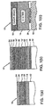
- the structure of a typical thin film disk is multilayered and includes a substrate at its base covered by an underlayer, a magnetic layer and optionally, an overlayer at the top.
- the overlayer may be coated with an overcoat and an organic lubricant.
- the magnetic layer is the main body on. which the magnetic bits are recorded.
- Longitudinal recording media comprised of cobalt or cobalt alloy-based magnetic films having a chromium or chromium alloy-based underlayer deposited on a nonmagnetic substrate have become the industry standard.
- Hc coercivity
- Mr remanent magnetization
- S* coercive squareness
- the Co alloy thin film should have uniform small grains with grain boundaries which can magnetically isolate neighboring grains. This kind of microstructure and crystallographic texture is normally achieved by manipulating the deposition process, by grooving the substrate surface, or most often by the proper use'of an underlayer.
- Underlayers can strongly influence the crystallographic orientation, the grain size and chemical segregation at the Co alloy, grain boundaries.
- a thin film layer which is sometimes called a precoat or a seed layer, is commonly deposited between the substrate and the underlayer to isolate the underlayer from possible substrate contaminants.
- Materials used for this layer with varying degrees of success include Al, Ti, Ni 3 P, TiSi 2 , Cr, C, Ta, Wand Zr.
- a (1120) bicrystalline longitudinal magnetic recording medium, CoCrPt/Cr, formed on a MgO single crystal disk substrate is described in M. Futamoto et al., "Magnetic and recording characteristic of bicrystalline longitudinal recording media formed on an MgO single crystal disc substrate", IEEE Transactions on Magnetics, Vol. 30, No. 6, p.3975 (1994). Because of the anisotropic magnetic properties and hence, the recording properties, around the circumference of the single crystal disk, this disk is of limited utility.
- United States Patent No. 4833020 discloses, in a magnetic recording medium including an underlayer and a magnetic layer formed sequentially on a substrate, the underlayer is composed of a composite underlayer having an at least two-layered structure, the underlayer on the side of the substrate is made of a material providing low modulation to the magnetic recording medium while the underlayer on the side of the magnetic layer is made of a material providing a high S/N ratio to the medium. This makes it possible to obtain a magnetic recording medium having low modulation and high S/N ratio.
- a magnetic recording medium having a substrate, an underlayer and a magnetic layer, wherein said underlayer has an (002) texture and wherein a seed layer is disposed between said substrate and said underlayer, said seed layer comprising polycrystalline MgO having an (002) texture sputter deposited on said substrate for promoting the (002) texture in said underlayer.
- Another aspect of the present invention provides an apparatus for recording and reading magnetic data comprising:
- a further aspect of the present invention provides a method of producing an oriented underlayer between a substrate and a magnetic layer in a magnetic media comprising:
- the present invention is concerned with recording media incorporated in a disc drive having a rotatable disc for operation in conjunction with magnetic transducing heads for the recording and reading of magnetic data.
- the recording medium has a novel seed layer on which to induce the (002) crystallographic texture in an underlayer for the magnetic film of the medium.
- the magnetic recording medium of the present invention comprises a substrate, a magnetic layer, preferably formed from Co or Co alloy film, and a seed layer comprising a material having a B1- ordered crystalline structure with a (002) texture, formed of MgO, sputter deposited on the substrate.
- An underlayer is also provided which preferably comprises a material having either an A2 structure or a B2- ordered crystalline structure disposed between the seed layer and the magnetic layer.
- the A2 phase is preferably Cr or a Cr alloy, such as CrV.
- the B2 phase is selected from the group consisting of NiAl, AlCo, FeAl, FeTi, CoFe, CoTi, CoHf. CoZr, NiTi, CuBe, CuZn, AlMn, AlRe, AgMg, and Al 2 FeMn 2 , and is most preferably FeAl or NiAl.
- the underlayer may be formed in multiple layers wherein each layer is a different one of the foregoing materials.
- the Co or Co alloy preferably used as the magnetic layer has a hexagonal close packed (HCP) structure and is preferably deposited with its c-axis, the magnetic easy axis (the direction in which it is easily magnetized), substantially parallel to the plane of the magnetic layer.
- HCP hexagonal close packed
- the recording medium may also include a chromium or chromium alloy intermediate layer interposed between the magnetic layer and the underlayer.
- the intermediate layer is relatively thin, preferably between about 10 to 500 ⁇ (1 to 50 nm). Thinner layers can provide some improvement provided the layer is thick enough to form a substantially continuous layer on the surface of the underlayer.
- the magnetic layer may be covered by an overlayer which in turn may be covered by an overcoat.
- An organic lubricant is preferably added over the overcoat.
- first magnetic layer there may be a first magnetic layer and a second magnetic layer with one or more interlayers disposed between the two magnetic layers.
- the interlayer is typically Cr, of about 10 to 40 ⁇ (1 to 4 nm).
- the second magnetic layer may be covered by the overlayer/overcoat/lubricant layers described above.
- BCC body centered cubic
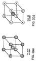
- NiAl for example, is a Hume-Rothery ⁇ -phase electron compound with a valence electron/atom ratio of 3/2 which gives a B2 crystalline structure, shown in Fig. 2(b).
- NiAl has a lattice constant of 0.2887nm, almost identical to that of Cr, 0.2884nm.
- the Co or Co alloy films By placing the B2- orderec structure on the substrate, below the magnetic layer, the Co or Co alloy films, when deposited, either directly or through an intermediate Cr or Cr alloy layer, grow epitaxially at the B2 interface and reorient the HCP c-axis away from being random or normal to the film plane, yielding a stable, improved thin film microstructure with magnetic properties which are particularly well suited to high density recording.
- NiAl for example, maintains its B2 structure stable up to the melting point of 1911K and the structure does not change over a wide composition range from 41.5 to 55 at% Al at 673K. Strong bonding between the metallic atoms slows the atomic mobility during the film's deposition thereby yielding a smaller grain size film than is present with the Cr underlayer.
- a small grain size can benefit the recording properties of the media by increasing the number of grains per unit area and hence, lowering the media noise.
- NiAl is nonmagnetic with an extremely low magnetic susceptibility, on the order of 2x10 -7 to 5x10 -7 emu/g, has good thermal conductivity, high stiffness, and good environmental corrosion resistance.
- the recording medium of the invention may be a rigid magnetic disc rotatable about an axis that is incorporated into a disc drive (not shown).
- the disc drive includes a magnetic transducing head, or slider, which is supported on a movable arm which is in turn part of a suspension assembly for moving the head over the surface of the disc.
- the transducing head when moving over the surface of the disc during normal operation, is maintained in a spaced, parallel relationship relative to the surface of the disc, in close proximity to the disc.
- a typical distance is 10 ⁇ in (2.54 ⁇ 10 -4 mm) or less.
- Disc drives such as this are standard equipment in the industry. See , Mee, C.D. and Daniel, E.D., MAGNETIC RECORDING, Vols.
- the magnetic recording media of the present invention may also be used with flexible magnetic discs using known flexible substrates.
- a magnetic recording medium which led to the recording medium of the present invention, for incorporation into disc drives, was comprised of a substrate 12, an underlayer 14 and a magnetic layer 16.
- a substrate 12 an underlayer 14 and a magnetic layer 16.
- an overcoat 20 as shown.
- An intermediate layer 22 of Cr may be disposed between the underlayer 14 and the magnetic layer 16.
- An organic lubricant 24 is preferably applied to the overcoat 20.
- first and second magnetic layers 16' and 16"
- interlayers 30 disposed between the first magnetic layer 16' and a second magnetic layer 16''.
- the interlayer 30 is preferably made of Cr and is 1nm to 4nm (10 to 40 ⁇ ) thick.
- the second magnetic layer 16'' is covered by an overlayer 18, the overcoat 20, and the organic lubricant 24 shown in Fig. 1(a).
- a seed layer 28 1.0nm to 50nm (10 to 500 ⁇ ) thick is disposed between the substrate 12 and the underlayer 14 to nucleate growth.
- the seed layer 28 is made of MgO.
- the seed layer 28 is MgO having B1- ordered crystalline structure with a (002) texture sputter deposited on the substrate beneath the underlayer.
- the seed layer forms a substantially continuous layer up to 50nm in thickness, and preferably up to 20nm in thickness.
- the seed layer is 1.0nm to 50nm (10 to 500 ⁇ ) in thickness, and preferably between 1.0nm to 20nm (10 to 200 ⁇ ) in thickness, more preferably 2.5 to 20nm (25 to 200 ⁇ ) in thickness, and most preferably between 2.5nm to 10nm (25 to 100 ⁇ ) in thickness.
- the substrate 12 is formed of a nonmagnetic material, such as glass, silicon or an aluminum alloy coated with NiP.
- a nonmagnetic material such as glass, silicon or an aluminum alloy coated with NiP.
- Alternative hard disk substrates such as canasite, or SiC may be used.
- the magnetic layers 16, 16' and 16" are deposited with the longitudinal magnetic easy axis thereof substantially parallel to the plane of such magnetic layer, are preferably a Co or Co alloy film, such as CoCr, SmCo, CoP, CoPt, CoNiCr, CoNiPt, CoCrTaSi, CoCrPtSi, CoCrPtB, CoCrPtTa, or other known Co alloy magnetic films and are each 5 - 60nm (50 - 600 ⁇ ) thick.
- a Co or Co alloy film such as CoCr, SmCo, CoP, CoPt, CoNiCr, CoNiPt, CoCrTaSi, CoCrPtSi, CoCrPtB, CoCrPtTa, or other known Co alloy magnetic films and are each 5 - 60nm (50 - 600 ⁇ ) thick.
- the B2- ordered crystalline structure of the underlayer 14 is shown in Fig. 2(b).
- the underlayer 14 is most preferably NiAl. It is 10 - 200nm (100 - 2000 ⁇ ) thick.
- the underlayer may be FeAl, or multiple layers, alternating between a NiAl layer and a FeAl layer.
- a multiple layer having a first layer of NiAl and a second layer of FeAl, AlCo, FeTi, CoFe, CoTi, CoHf, CoZr, NiTi, CuBe, CuZn, AlMn, AlRe, AgMg or Al 2 FeMn 2 may be used.
- Various combinations of multiple layers wherein each layer is one of the B2- ordered crystalline phases may be employed as the underlayer of the present invention.
- the underlayer may be the B2- ordered material described above or may be an A2 structure, such as Cr or a Cr alloy, such as CrV.
- An overlayer 18, which is thought to prevent corrosion, may be provided adjacent to and preferably in contact with the magnetic layer 16 or 16''.
- the overlayer 18 is 1 - 10nm (10-100 ⁇ ) thick and may be made of W, Ta, Zr, Ti, Y, Pt, Cr or any combination thereof.
- An overcoat 20 may be provided external to the overlayer 18, so that the overlayer 18 is positioned between the magnetic layer 16 or 16" and the overcoat 20, as shown in Figs. 1(a) and (b).
- the overcoat provides a mechanical wear layer and is 2.5 - 30nm (25-300 ⁇ ) thick. It is preferably made of a ceramic material or diamond like carbon, such as SiO 2 , SiC, CN, ZrO 2 or C.
- An organic lubricant 24 may be disposed on the overcoat 20.
- the lubricant is 1nm to 30nm (10 to 300 ⁇ ) thick and is preferably a fluoro-chlorocarbon or a perfluoroether.
- Examples include CCl 2 FCClF 2 , CF 3 (CF 2 ) 4 CF 3 , CF 3 (CF 2 ) 5 CF 3 , CF 3 (CF 2 ) 10 CF 3 , and CF 3 (CF 2 ) 16 CF 3 .
- CoCrTa and CoCrPt films were sputter-deposited onto Cr or NiAl underlayers on glass substrates by techniques well known to those skilled in the art. Vibrating sample magnetometry (VSM) was used to measure the magnetic properties. In the following experimental examples, RF diode sputtering was used for film deposition onto smooth glass substrates which were not mechanically textured.
- VSM Vibrating sample magnetometry
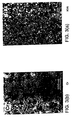
- a 100nm NiAl film was deposited onto a glass substrate. Its microstructure, as observed by transmission electron microscopy (TEM), is compared with a similarly deposited Cr film and shown in Figs. 3a and 3b.
- the NiAl film, Fig. 3a shows a grain size of about 15nm which is noticeably smaller (about 50%) than the grain size of the similarly sputter deposited Cr film, Fig. 3b.
- the grain size of the underlayer strongly influences the grain size of the Co based magnetic layer. It is believed that the strong atomic bonding within the two atom structure of NiAl inhibits the mobility of the Ni and Al atoms and so limits the growth of the grains.
- the small, well faceted grains of NiAl promote the formation of smaller, more well defined grains in the magnetic layer. Smaller grains reduce noise in the recording media.
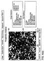
- a roughness analysis was done also using an atomic force microscope (AFM).
- the AFM uses an extremely small sharp tip to scan the sample surface and measures the atomic attraction between the sharp tip and the surface of the sample. The AFM can thereby determine on a very small scale the topology of the sample surface.
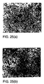
- the white and dark areas of Figs. 4(a) and (b) represent height differences of the NiAl and Cr underlayer films, respectively, of 100nm thickness.
- the images clearly show that the grains (diameter of bumps) of the NiAl films, Fig. 4(a) are much smaller and more uniform than are the Cr grains, Fig. 4(b). Small and uniform grains implies lower noise if everything else about the media is equal.
- the roughness is a measure of the vertical height variations as one scans over the sample surface.
- the root mean square (RMS) and mean (average) roughness (Ra) are two different ways of calculating the roughness from the same data. While the maximum height (Rmax) can be misleading if there is a bad spot on the sample, it is a good indication of the extremes (lack of uniformity) of the roughness if the sample is good.
- the roughness difference between the NiAl and the Cr is another indication of the larger variation in the Cr grain size.
- the image statistics for the NiAl film show an RMS roughness of 0.372nm, a mean roughness (Ra) of 0.296nm and a maximum height (Rmax) of 2.798nm.
- the Cr film shows RMS roughness of 0.722nm, a mean roughness (Ra) of 0.581nm and a maximum height (Rmax) of 4.914nm.
- the Cr underlayer has both larger grains and is considerably rougher than the NiAl film.
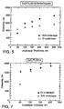
- CoCrTa films were deposited onto NiAl and Cr underlayers of various thickness on glass substrates.
- the in-plane coercivities of the magnetic films were plotted as a function of the underlayer thickness.
- the underlayer is greater than 100nm thick, the CoCrTa/NiAl films have a higher coercivity, Hc, than the CoCrTa/Cr films for comparable thicknesses.
- Hc coercivity
- the coercivity increases and then reaches a plateau as the underlayer thickens.
- the steady increase is indicative of larger grains. As indicated previously, larger grains also cause increased noise.
- the increased grain size causes a much rougher surface which interferes with the ability of the magnetic head, or transducer, to get close to and read the disk.
- the underlayer is not made any thicker than it has to be to get the desired improvement in coercivity.
- the recording medium having the NiAl underlayer offers greater coercivity at thicknesses equal to or even slightly less than those of a recording medium having a Cr underlayer.
- the NiAl underlayer offers comparable coercivities and smaller grains than the recording media having a Cr underlayer.
- the recording medium has a better in-plane c-axis film crystallographic texture when NiAl is used as the underlayer than it does when Cr is the underlayer.
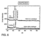
- the NiAl film has its ⁇ 110 ⁇ and ⁇ 112 ⁇ planes preferentially oriented parallel to the film plane. This is supported by X-ray diffraction studies which show that the CoCrTa film on the NiAl underlayer has a larger (10 1 0) Co peak than the CoCrTa film on a Cr underlayer.
- Fig. 6 provides a comparison of x-ray diffraction spectra of the CoCrTa/NiAl and CoCrTa/Cr films with their Hc values marked on each curve.
- the NiAl spectrum has a much stronger HCP Co (10 1 0) peak adjacent the NiAl (110) peak which is believed to reflect a (112) NiAl texture which is weak or not present at all in the Cr underlayer.
- FIG. 8 is the x-ray diffraction spectra of CoCrPt/NiAl and CoCrPt/Cr films which show that the CoCrPt film on the NiAl underlayer has a stronger (10 1 0) Co peak than does the same film on Cr underlayer, which again is an indication of a better in-plane c-axis film crystallographic texture.
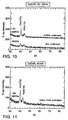
- Fig. 11 demonstrates that another phase with the B2-structure, FeAl, also produces a strong (10 1 0) Co peak. Pt is added to Co alloys to improve coercivity, but at a 15 - 20% Pt content, the magnetic layer does not lattice match well with the Cr underlayer.
- Fig. 8 also shows a (0002) Co peak, which reflects a poor epitaxial growth to the Cr underlayer. This phenomenon does not appear to take place when the NiAl is used as the underlayer.
- the NiAl and FeAl spectra reveal a strong (10 1 0) Co peak and the absence of the (0002) peak, which is indicative of a good longitudinal structure.
- NiAl has not been heretofore used as an underlayer for thin film longitudinal magnetic recording media.
- the sputter deposited NiAl films have small grain size and enhance the Co alloy films' ⁇ 10 1 0 ⁇ texture.
- the underlayers of the present invention enhance the in plane c-axis orientation and therefore improve the magnetic properties of the thin film disk with a glass substrate. Similar improvements can be found when other substrates, such as aluminum alloy substrates coated with NiP or silicon substrates are used. Similar results on alternative hard disk substrates such as canasite, or SiC should be obtained also.
- the underlayer of the present invention may be used as the underlayer for other Co alloy thin films, such as CoCr, SmCo, CoP, CoPt, CoNiCr, CoNiPt, CoCrTaSi, CoCrPtSi, CoCrPtB, and CoCrPtTa.
- Co alloy thin films such as CoCr, SmCo, CoP, CoPt, CoNiCr, CoNiPt, CoCrTaSi, CoCrPtSi, CoCrPtB, and CoCrPtTa.
- FIG. 9 shows the x-ray spectra of a CoCrTa/NiAl film with and without a 2.5nm Cr intermediate layer between the CoCrTa layer and the NiAl layers. From Fig. 9 it is apparent that when a very thin layer of Cr is placed between NiAl and CoCrTa, the high quality texture of the Co (10 1 0) is maintained and the coercivity is improved.
- an intermediate layer 22 of Cr having a thickness less than about 1.0nm does not form a continuous layer.
- a substantially continuous layer is apparently needed to give consistent results.
- the improved coercivity is marked and consistent.
- Thicknesses above 5.0nm continue to provide good coercivity, but produce no significant improvement.
- the combination of a CoCrPt magnetic layer, a NiAl underlayer and a very thin (about 2.5nm) Cr intermediate layer disposed between the magnetic layer and the underlayer increases the coercivity even more significantly, by 450 Oe. If the cobalt alloy magnetic layer has only the 2.5nm thick Cr layer without the NiAl underlayer, the Co layer tends to remain either face centered cubic (FCC) or orients [0001] perpendicular to the plane of the film.
- FCC face centered cubic
- Fig. 10 shows the x-ray spectra of a CoCrPt/NiAl film with and without a 2.5nm Cr intermediate layer between the CoCrPt layer and the NiAl layer.
- the increase in coercivity is even more dramatic than the increase shown in Fig. 9 using a CoCrTa magnetic layer.
- the lattice constant of the cobalt HCP structure is significantly increased when the larger Pt atom is substituted for Co. Hence a poorer lattice match between the CoCrPt and the underlayer results.
- the underlayers were sputter deposited on a glass substrate without bias and the magnetic layer was sputter deposited with bias, i.e. with an applied voltage to the surface.
- the disk represented by squares was CoCrTa/Cr having a coercivity of 1700 Oe.
- the disk represented by circles was CoCrTa/NiAl having a coercivity of 1400 Oe.
- the disks having NiAl as the underlayer were determined to behave comparably to the disks having Cr as the underlayer, but the coercivities were somewhat lower in this sample for NiAl films,when the magnetic layer is deposited with bias. The noise levels were also somewhat lower.
- Fig. 15 The disk represented by the squares had a CoCrTa magnetic layer on a Cr underlayer and a coercivity of 1000 Oe.
- the disk represented by circles had a CoCrTa magnetic layer and a NiAl underlayer and a coercivity of 1150 Oe. Again, the behavior of the two disks was comparable with the NiAl disk showing lower noise somewhat.
- Fig. 16 plots the medium integrated noise power (MNP) as a function of linear recording density.
- the MNP represents the total integrated noise power divided by the voltage pulse one would obtain if the signal were recorded at low frequencies (i.e., the isolated pulse height).
- Fig. 16 shows the results for the disks of Fig. 14.
- Fig. 17 plots the MNP as a function of linear density for the disks of Fig. 15. The results for the disks in Figs. 16 and 17 are comparable, with lower noise for the disk having the NiAl underlayer, particularly when the magnetic layer is not deposited with bias.
- the magnetic recording media has a seed layer sputter deposited on the substrate beneath the underlayer, it has been found that thin layers of MgO with a B1- ordered crystalline structure and (002) film texture improve the texture and magnetic properties of the Co and Co alloy thin films.
- the MgO seed layer may be used to enhance the-texture of underlayers comprised of either the A2 structure, such as Cr, or the B2- ordered structures, such as NiAl, AlCo, FeAl, FeTi, CoFe, CoTi, CoHf, CoZr, NiTi, CuBe, CuZn, AlMn, AlRe, AgMg and Al 2 FeMn 2 .
- MgO is an ionic crystal which has the B1 (NaCl-type) crystal structure with a lattice constant of 0.421nm (Fig. 18). It has excellent high temperature chemical stability. The melting point is nearly 3000°C.
- the strong (002) textured polycrystalline MgO film with random in-plane orientation provided by this embodiment of the recording media of the invention is of greater practical utility than the MgO single crystal disk substrates studied by M. Futamoto et al., "Magnetic and recording characteristic of bicrystalline longitudinal recording media formed on an MgO single crystal disc substrate", IEEE Transactions on Magnetics, Vol. 30, No. 6, p.3975 (1994).
- the films' thicknesses were also crosschecked with a Tencor profilometer. Surface morphology of the films were checked by atomic force microscopy and the bulk magnetic properties were measured by vibrating sample magnetometry. Crystallographic textures were studied by x-ray diffractometry with CuK ⁇ radiation.
- the sputter-deposited MgO films easily grow to have the (002) film texture. It is believed that the (002) preferential orientation is because the closest packed (002) plane has the lowest surface energy.
- the resulting texture of the underlayers is a strong (002), whether or not the substrate is heated. This is the often sought-after underlayer texture because the (11 2 0) textured Co alloy magnetic film layer tends to grow epitaxially on it.
- the use of sputter deposited MgO seed layers promotes the desired (002) texture in the Cr or NiAl underlayers without resorting to an external substrate heating device.
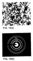
- Fig. 19 shows the transmission electron microscopy (TEM) bright field micrograph of a 100nm thick MgO film and its electron diffraction ring pattern.
- the ring pattern matches well with the expected diffraction pattern of a B1 polycrystalline material with a lattice constant of 0.423nm.
- the grain size is estimated to be about 45nm.
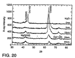
- Fig. 20 is a plot of the x-ray diffraction spectra of the CoCrPt(40nm)/Cr(100nm) films with various thicknesses of MgO seed layers. All film with MgO seed layers show Cr (002) and Co (11 2 0) peaks while the film without the seed layer does not have any reflections which indicate that there is in-plane c-axis texture.
- the visible Co (0002) peak in the diffraction spectrum of the film without a MgO seed layer is a manifestation of the large lattice misfit of Cr (110) to the Co (10 1 0) or Co (10 1 1) lattice plane or between Cr (002) to the Co (1120) lattice plane.
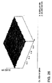
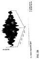
- Micro-bumps of up to 40nm in height and 200nm in diameter were observed in the 50nm thick MgO film shown in Fig. 28. Too great an increase in roughness causes the deterioration of the epitaxy of the MgO and Cr. However, magnetic media surface roughness due to MgO bumps of about 50 to about 200 ⁇ are advantageous in preventing the slider heads from sticking to the disc. Currently, disc surfaces are intentionally roughened mechanically with sand paper or by laser texturing to prevent such sticking. The sandpaper method is difficult to control.
- the MgO seed layer provides a dual use readily controlled roughness texture.
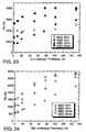
- Fig. 23 plots the in-plane coercivity values of the CoCrPt(40nm)/Cr films of various Cr underlayer thicknesses with and without MgO seed layers on glass substrates.
- Table I lists a complete set of in-plane magnetic properties of the CoCrPt(40nm)/Cr(100nm) films on MgO seed layers of various thicknesses.
- the improvement in coercivity increases as the thickness of the Cr underlayer or the MgO seed layer increases.
- the coercivity reaches a value as high as 4000 Oe, if a 50nm thick MgO seed layer is used along with a Cr underlayer thicker than 75nm. It is known that micro-bumps underneath the Co alloy film can increase the physical separation between the Co alloy grains and therefore increase the coercivity value. On the other hand, decreasing the Co (11 2 0) texture which is caused by the increasing roughness of the film would tend to decrease the coercivity.
- the multi-layered films in these experiments were made by sputtering one layer after the other without breaking the vacuum of the sputtering system.
- glass substrates with presputtered MgO seed layers can still induce good (002) Cr epitaxial growth even though the MgO films have been intentionally exposed to air for more than a month. This may be very convenient for media production where the MgO could be deposited in a separate vacuum system.
- Table II lists the VSM measurements of the 40nm thick CoCrPt films on 100nm NiAl underlayers on MgO seed layers of various thicknesses.
- the coercivity is shown to increase rapidly and then to level off as the MgO seed layer thickens.
- the crystallographic texture of these 40nm CoCrPt/100nm NiAl films on MgO seed layers revealed by x-ray diffraction spectra are plotted in Fig. 21.
- the (002) MgO peak continuously becomes Stronger as the MgO layer thickens.
- the intensity of the (002) NiAl peak is not proportional to the MgO thickness.
- the maximum coercivity film in Table II corresponds to the film with the strongest (002) NiAl crystallographic texture.
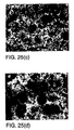
- FIG. 30 (a) and (b) show AFM surface topography plots of 100nm NiAl films on 10nm and 20nm MgO seed layers on glass substrates.
- the plots demonstrate that a 20nm MgO seed layer can roughen the film considerably to form surface bumps up to about 150nm in diameter and about 25nm in height. It is believed that the high density recording media of the future will need a low flying height. Notwithstanding the fact that the surface of the disc substrate is generally roughened by mechanical or chemical texturing to avoid having the transducer head stick to the smooth disc, the roughness of the 20nm MgO thickness may be problematic for high density recording media.
- the MgO seed layer can be used to tailor the roughness by controlling the MgO layer thickness, the deposition temperature and the sputtering process.
- Fig. 24 is a plot of four sets of coercivity data of the 40nm thick CoCrPt films with varying NiAl underlayer thicknesses for MgO seed layer thicknesses of 0nm, 5nm, 20nm and 50nm.
- Table III lists the in-plane bulk magnetic properties of the specimens depicted in Fig. 22.
- the data show that the coercivity of the CoCrPt film on the NiAl underlayer is significantly increased due to the incorporation of the Cr seed layer, similar to the MgO seed layer.
- Fig. 29 compares the TEM bright field micrographs of 40nm CoCrPt/100nm NiAl films on Snm MgO and 10nm Cr seed layers. Although these plane view micrographs show overlapping NiAl and Co grains, it is apparent that the grain size of the film with a Cr seed layer is more than twice the grain size (180 ⁇ ) of the film with a MgO seed layer, most likely due to the fact that added heat is not required in the process of the deposition of the MgO seed layer.
- Seed layers of Cr and MgO have been shown to induce the (002) crystallographic texture in the NiAl underlayers which has been shown to be beneficial to the in-plane coercivity of the CoCrPt films.
- the MgO seed layer does not require heating and therefore, have finer underlayer grains.
- a sputter deposited thin MgO seed layer with the (002) crystallographic texture induces the (002) texture in both the Cr and NiAl underlayer which in turn induces the (11 2 0) texture in the CoCrPt magnetic layer.
- the in-plane magnetic properties can be improved without resorting to external substrate heating.
- the Co alloy films provide greatly improved high density recording media.
- the surface roughness of the MgO seed layer can be controlled.
- the surface roughness of the recording medium can be controlled by the roughness of the MgO layer.
Landscapes
- Engineering & Computer Science (AREA)
- Manufacturing & Machinery (AREA)
- Magnetic Record Carriers (AREA)
Description
| The in-plane magnetic properties of the CoCrPt(40nm)/Cr(100nm) films on MgO seed layers of various thicknesses. | ||||
| MgO thickness | Hc, Oe | S (Mr/Ms) | S* | Mrt, memu/cm2 |
| 0nm | 2286 | 0.83 | 0.84 | 1.2 |
| 5nm | 2583 | 0.87 | 0.88 | 1.2 |
| 10nm | 2608 | 0.86 | 0.91 | 1.2 |
| 20nm | 3252 | 0.88 | 0.90 | 1.2 |
| 50nm | 4036 | 0.88 | 0.88 | 1.1 |
| The in-plane magnetic properties of the CoCrPt(40nm)/NiAl(100nm) films on MgO seed layers of various thickness. | ||||
| MgO thickness | Hc, Oe | S* | S | Mrt, memu/cm2 |
| 0nm | 1862 | 0.87 | 0.84 | 1.4 |
| 2nm | 2558 | 0.92 | 0.86 | 1.1 |
| 5nm. | 2811 | 0.92 | 0.87 | 1.2 |
| 8nm | 3283 | 0.92 | 0.88 | 1.1 |
| 10nm | 3238 | 0.91 | 0.87 | 1.0 |
| 20nm | 3236 | 0.86 | 0.84 | 1.0 |
| 50nm | 3182 | 0.82 | 0.87 | 1.0 |
| The in-plane magnetic properties of the 40nm CoCrPt films on 100nm NiAl, 100nm Cr and 100nm NiAl/10nm Cr underlayers. | ||||
| Underlayer | Hc, Oe | S* | S | Mrt, memu/cm2 |
| NiAl | 2221 | 0.79 | 0.81 | 0.81 |
| Cr | 2228 | 0.74 | 0.88 | 0.83 |
| NiAl/Cr | 3153 | 0.78 | 0.85 | 0.84 |
Claims (26)
- A magnetic recording medium having a substrate, an underlayer and a magnetic layer, wherein said underlayer has an (002) texture and wherein a seed layer is disposed between said substrate and said underlayer, said seed layer comprising polycrystalline MgO having an (002) texture sputter deposited on said substrate for promoting the (002) texture in said underlayer.
- A medium according to Claim 1, wherein said seed layer is from 1.0nm to 50nm thick.
- A medium according to Claim 2, wherein said seed layer is from 2.5 to 20nm thick.
- A medium according to any one of Claims 1 to 3, wherein said seed layer forms a substantially continuous layer.
- A medium according to any one of Claims 1 to 4, which also includes a chromium or chromium alloy intermediate layer interposed between said magnetic layer and said underlayer.
- A medium according to Claim 5, wherein said intermediate layer is from 1.0nm to 5.0nm thick.
- A medium according to any one of Claims 1 to 6, wherein the underlayer comprises Cr, a Cr alloy having an A2 crystalline structure or material having a B2 crystalline structure.
- A medium according to any one of Claims 1 to 6, wherein said underlayer comprises a material selected from Cr, CrV, NiAl, AlCo, FeAl, FeTi, CoFe, CoTi, CoHf, CoZr, NiTi, CuBe, CuZn, AlMn, AlRe, AgMg and Al2FeMn2, and the magnetic layer comprises Co or a Co alloy film.
- A medium according to Claim 8, wherein said underlayer comprises a material selected from NiAl and FeAl.
- A medium according to any preceding claim, wherein said underlayer comprises multiple layers of two or more of said materials.
- A medium according to any preceding claim, wherein the magnetic layer comprises a Co or Co alloy film.
- A medium according to any preceding claim, wherein said magnetic layer has a (1120) texture expitaxially grown from said underlayer.
- A medium according to any preceding claim, which also includes an overcoat disposed on the magnetic layer, such that said magnetic layer lies between said underlayer and said overcoat.
- A medium according to Claim 13, which also includes an organic lubricant disposed on said overcoat such that said overcoat lies between said lubricant and said magnetic layer.
- A medium according to any preceding claim, which also includes an overlayer disposed on said. magnetic layer such that said overlayer lies between said magnetic layer and said overcoat.
- A medium according to any preceding claim, wherein said seed layer has a surface adjacent said underlayer, said seed layer surface being roughened to effect a surface roughness of 50 to 200Å in said magnetic layer.
- An apparatus for recording and reading magnetic data comprising:a rotatable disc, said disc comprising a substrate, a seed layer comprised of polycrystalline MgO having an (002) texture sputter deposited on said substrate, a Co or Co alloy film forming a magnetic layer, and an underlayer comprising Cr, a Cr alloy having an A2 crystalline structure or material having a B2 crystalline structure disposed between said seed layer and said magnetic layer, said underlayer having an (002) texture;a magnetic transducing head; andmeans for supporting said head in close proximity to said disc and said magnetic layer for controlled movement of said head relative to said disc.
- An apparatus according to Claim 17, wherein said underlayer comprises a material selected from NiAl, AlCo, FeAl, FeTi, CoFe, CoHf, CoZr, NiTi, CuBe, CuZn, AlMn, AlRe, AgMg and Al2FeMn2.
- The apparatus according to Claim 17, wherein said underlayer comprises a material selected from NiAl and FeAl.
- An apparatus according to any one of Claims 17 to 19, wherein said magnetic layer has a (1120) texture epitaxially grown from said underlayer.
- An apparatus according to any one of Claims 17 to 20, wherein said seed layer is from 1.0nm to 50nm thick.
- An apparatus according to any one of Claims 17 to 21, wherein said disc also includes a chromium or chromium alloy intermediate layer interposed between said magnetic layer and said underlayer of said disc.
- A method of producing an oriented underlayer between a substrate and a magnetic layer in a magnetic media comprising:sputtering MgO onto the substrate to form a polycrystalline seed layer having a (002) texture; anddepositing an underlayer comprising of Cr or a Cr alloy having an A2 structure or material having a B2 structure, wherein the underlayer has an (002) texture and is disposed between the seed layer and the magnetic layer.
- A method according to Claim 23, which also includes forming a Co or Co alloy magnetic layer.
- A method according to Claim 23 or 24, wherein the step of depositing an underlayer comprises depositing an underlayer comprising a material selected from Cr, CrV, NiAl, AiCo, FeAl, FeTi, CoFe, CoTi, CoHf, CoZr, NiTi, CuBe, CuZn, AlMn, AlRe, AgMg and Al2FeMn2; and the magnetic layer having a (1120) texture is formed on the underlayer.
- A method according to Claim 23, 24 or 25, wherein said step of sputtering comprises radio frequency diode sputtering.
Applications Claiming Priority (2)
| Application Number | Priority Date | Filing Date | Title |
|---|---|---|---|
| US553893 | 1990-07-16 | ||
| US08/553,893 US5800931A (en) | 1994-09-29 | 1995-11-06 | Magnetic recording medium with a MgO sputter deposited seed layer |
Publications (2)
| Publication Number | Publication Date |
|---|---|
| EP0772188A1 EP0772188A1 (en) | 1997-05-07 |
| EP0772188B1 true EP0772188B1 (en) | 2002-05-08 |
Family
ID=24211201
Family Applications (1)
| Application Number | Title | Priority Date | Filing Date |
|---|---|---|---|
| EP96307994A Expired - Lifetime EP0772188B1 (en) | 1995-11-06 | 1996-11-05 | Magnetic recording medium with a MgO sputter deposited seed layer |
Country Status (4)
| Country | Link |
|---|---|
| US (1) | US5800931A (en) |
| EP (1) | EP0772188B1 (en) |
| DE (1) | DE69621099T2 (en) |
| SG (1) | SG43435A1 (en) |
Cited By (1)
| Publication number | Priority date | Publication date | Assignee | Title |
|---|---|---|---|---|
| CN110116376A (en) * | 2019-06-21 | 2019-08-13 | 广东工业大学 | A kind of metallic bond grinding tool and preparation method thereof |
Families Citing this family (48)
| Publication number | Priority date | Publication date | Assignee | Title |
|---|---|---|---|---|
| US6077603A (en) * | 1996-07-03 | 2000-06-20 | Seagate Technology, Inc. | Seeded underlayer in magnetic thin films |
| JP2924798B2 (en) * | 1996-07-12 | 1999-07-26 | 日本電気株式会社 | Magnetoresistance thin film |
| JP3022909B2 (en) * | 1996-10-07 | 2000-03-21 | 富士電機株式会社 | Magnetic recording medium and method of manufacturing the same |
| SG65718A1 (en) * | 1996-12-27 | 1999-06-22 | Hoya Corp | Glass substrate for information recording medium method of manufacturing the substrate magnetic recording medium using the glass substrate and method of manufacturing the medium |
| JPH10233016A (en) * | 1997-02-21 | 1998-09-02 | Hitachi Ltd | In-plane magnetic recording medium and magnetic storage device using the same |
| US6027801A (en) * | 1997-04-04 | 2000-02-22 | Hitachi Maxell, Ltd. | Magnetic recording medium |
| JPH10326417A (en) * | 1997-05-26 | 1998-12-08 | Toshiba Corp | Magnetic disk and magnetic disk drive |
| JP3803180B2 (en) * | 1997-09-25 | 2006-08-02 | 富士通株式会社 | Magnetic recording medium, method for manufacturing the same, and magnetic disk drive |
| US6248416B1 (en) * | 1997-11-10 | 2001-06-19 | Carnegie Mellon University | Highly oriented magnetic thin films, recording media, transducers, devices made therefrom and methods of making |
| JP2950301B2 (en) * | 1997-11-21 | 1999-09-20 | 日本電気株式会社 | Magnetic disk drive |
| US6156422A (en) * | 1997-12-12 | 2000-12-05 | Seagate Technology, Inc. | High density magnetic recording medium with high Hr and low Mrt |
| US6207269B1 (en) * | 1997-12-12 | 2001-03-27 | Seagate Technology Llc | High substrate bias sputtering underlayer for longitudinal recording media |
| US6218003B1 (en) * | 1998-02-10 | 2001-04-17 | Seagate Technology, Llc | Magnetic recording medium containing a Cr(TiO2) underlayer |
| US6228515B1 (en) * | 1998-02-17 | 2001-05-08 | Korea Institute Of Science And Technology | Underlayer for use in a high density magnetic recording media |
| JP4082785B2 (en) * | 1998-05-15 | 2008-04-30 | 富士通株式会社 | Magnetic recording medium and method for manufacturing the same |
| US6139950A (en) * | 1998-06-04 | 2000-10-31 | Seagate Technology Llc | Magnetic recording medium containing a Cr(HfO2) or Cr(ZrO2) |
| US6348276B1 (en) | 1998-09-25 | 2002-02-19 | Seagate Technology Llc | Magnetic recording media with a surface-oxidized nial sub-seedlayer |
| US6346339B1 (en) | 1998-09-30 | 2002-02-12 | Seagate Technology Llc | Magnetic recording media with a nialox sub-seedlayer |
| US6461750B1 (en) | 1998-09-30 | 2002-10-08 | Seagate Technology, Inc. | Magnetic recording medium with dual magnetic layers and high in-plane coercivity |
| US6383667B1 (en) | 1998-10-09 | 2002-05-07 | Hitachi, Ltd. | Magnetic recording medium |
| US6185081B1 (en) | 1999-06-30 | 2001-02-06 | Read-Rite Corporation | Bias layers which are formed on underlayers promoting in-plane alignment of the c-axis of cobalt used in magnetoresistive transducers |
| JP2001023142A (en) * | 1999-07-05 | 2001-01-26 | Sony Corp | Magnetic recording media |
| US6583953B1 (en) | 1999-07-12 | 2003-06-24 | Mark Lauer | Silicon carbide overcoats for information storage systems and method of making |
| US6416881B1 (en) | 1999-08-10 | 2002-07-09 | Seagate Technology Llc | Media with a metal oxide sealing layer |
| US6432563B1 (en) | 2000-04-03 | 2002-08-13 | Carnegie Mellon University | Zinc enhanced hard disk media |
| US6740397B1 (en) | 2000-05-24 | 2004-05-25 | Seagate Technology Llc | Subseedlayers for magnetic recording media |
| US6838188B1 (en) * | 2000-05-30 | 2005-01-04 | Maxtor Corporation | Magnetic recording medium having ternary or quaternary alloy seedlayer |
| US6596417B1 (en) | 2000-09-29 | 2003-07-22 | Carnegie Mellon University | Magnetic recording medium with a Ga3Pt5 structured underlayer and a cobalt-based magnetic layer |
| JP2002190108A (en) * | 2000-10-13 | 2002-07-05 | Fuji Electric Co Ltd | Magnetic recording medium and method of manufacturing the same |
| US7050274B2 (en) * | 2001-03-15 | 2006-05-23 | Seagate Technology Llc | Multilayer permanent magnet films |
| US7006328B2 (en) * | 2002-08-22 | 2006-02-28 | Showa Denko Kabushiki Kaisha | Magnetic recording medium, production process thereof, and magnetic recording and reproducing apparatus |
| AU2002334408A1 (en) * | 2002-09-06 | 2004-04-08 | Fujitsu Limited | Magnetic recording medium and magnetic storage apparatus |
| US6863993B1 (en) | 2003-09-30 | 2005-03-08 | Hitachi Global Storage Technologies Netherlands, B.V. | Thin film media with a dual seed layer of RuAI/NiAIB |
| US20050249981A1 (en) * | 2004-05-10 | 2005-11-10 | Heraeus, Inc. | Grain structure for magnetic recording media |
| WO2006033766A2 (en) * | 2004-08-25 | 2006-03-30 | The Regents Of The University Of Michigan | Dendrimer based compositions and methods of using the same |
| US20060042938A1 (en) * | 2004-09-01 | 2006-03-02 | Heraeus, Inc. | Sputter target material for improved magnetic layer |
| US20060286414A1 (en) * | 2005-06-15 | 2006-12-21 | Heraeus, Inc. | Enhanced oxide-containing sputter target alloy compositions |
| US20070041934A1 (en) * | 2005-08-12 | 2007-02-22 | Regents Of The University Of Michigan | Dendrimer based compositions and methods of using the same |
| US7993497B2 (en) * | 2005-11-21 | 2011-08-09 | Wd Media (Singapore) Pte. Ltd. | Magnetic disk and magnetic disk manufacturing method |
| US20070253103A1 (en) * | 2006-04-27 | 2007-11-01 | Heraeus, Inc. | Soft magnetic underlayer in magnetic media and soft magnetic alloy based sputter target |
| CA2684725A1 (en) * | 2007-04-19 | 2009-01-15 | The Regents Of The University Of Michigan | Dendrimer based compositions and methods of using the same |
| US7829208B2 (en) * | 2007-11-29 | 2010-11-09 | Seagate Technology Llc | Chromium nitride layer for magnetic recording medium |
| WO2009151687A2 (en) | 2008-03-12 | 2009-12-17 | The Regents Of The University Of Michigan | Dendrimer conjugates |
| US8611045B2 (en) * | 2011-09-29 | 2013-12-17 | Tdk Corporation | Magnetic recording apparatus |
| US8941950B2 (en) * | 2012-05-23 | 2015-01-27 | WD Media, LLC | Underlayers for heat assisted magnetic recording (HAMR) media |
| US9966096B2 (en) | 2014-11-18 | 2018-05-08 | Western Digital Technologies, Inc. | Self-assembled nanoparticles with polymeric and/or oligomeric ligands |
| CN107430872B (en) * | 2015-06-02 | 2019-07-30 | 富士电机株式会社 | Manufacturing method of magnetic recording medium |
| WO2017210324A1 (en) * | 2016-05-31 | 2017-12-07 | The Regents Of The University Of California | Synthesis of tetrataenite thin films via rapid thermal annealing |
Family Cites Families (19)
| Publication number | Priority date | Publication date | Assignee | Title |
|---|---|---|---|---|
| US3615911A (en) * | 1969-05-16 | 1971-10-26 | Bell Telephone Labor Inc | Sputtered magnetic films |
| DE2909891A1 (en) * | 1979-03-14 | 1980-09-25 | Basf Ag | MAGNETIC RECORDING CARRIER |
| DE3343107A1 (en) * | 1983-11-29 | 1985-06-05 | Basf Ag, 6700 Ludwigshafen | MAGNETIC RECORDING CARRIERS |
| US4735840A (en) * | 1985-11-12 | 1988-04-05 | Cyberdisk, Inc. | Magnetic recording disk and sputtering process and apparatus for producing same |
| US4652499A (en) * | 1986-04-29 | 1987-03-24 | International Business Machines | Magnetic recording medium with a chromium alloy underlayer and a cobalt-based magnetic layer |
| JPH07114016B2 (en) * | 1986-06-12 | 1995-12-06 | 株式会社東芝 | Magnetic recording medium and manufacturing method thereof |
| JP2791015B2 (en) * | 1986-12-24 | 1998-08-27 | 株式会社日立製作所 | Magnetic recording media |
| JP2561655B2 (en) * | 1987-01-29 | 1996-12-11 | 株式会社日立製作所 | In-plane magnetic recording medium |
| JPS63300508A (en) * | 1987-05-29 | 1988-12-07 | Nec Corp | Resin sealed semiconductor device |
| US5231294A (en) * | 1988-03-25 | 1993-07-27 | Hitachi, Ltd. | Manganese-aluminum and manganese-silicon magnetic films, and magnetic recording medium |
| US5147732A (en) * | 1988-09-28 | 1992-09-15 | Hitachi, Ltd. | Longitudinal magnetic recording media and magnetic memory units |
| US5192626A (en) * | 1988-12-14 | 1993-03-09 | Teijin Limited | Optical recording medium |
| US4902583A (en) * | 1989-03-06 | 1990-02-20 | Brucker Charles F | Thick deposited cobalt platinum magnetic film and method of fabrication thereof |
| JP2513893B2 (en) * | 1989-04-26 | 1996-07-03 | 日立金属株式会社 | Magnetic recording media |
| AU627965B2 (en) * | 1989-12-15 | 1992-09-03 | Inco Alloys International Inc. | Oxidation resistant low expansion superalloys |
| US5062021A (en) * | 1990-03-12 | 1991-10-29 | Magnetic Peripherals Inc. | Selectively textured magnetic recording media |
| US5057200A (en) * | 1990-08-15 | 1991-10-15 | Hmt Technology Corporation | Method of forming thin-film recording medium |
| US5344706A (en) * | 1991-10-01 | 1994-09-06 | Carnegie Mellon University | Magnetic recording medium comprising an underlayer and a cobalt samarium amorphous magnetic layer having a SmCo5 crystalline interface with the underlayer |
| US5363794A (en) * | 1992-12-02 | 1994-11-15 | The Board Of Trustees Of The Leland Stanford Junior University | Uniaxial thin film structures formed from oriented bilayers and multilayers |
-
1995
- 1995-11-06 US US08/553,893 patent/US5800931A/en not_active Expired - Lifetime
-
1996
- 1996-11-04 SG SG1996011004A patent/SG43435A1/en unknown
- 1996-11-05 EP EP96307994A patent/EP0772188B1/en not_active Expired - Lifetime
- 1996-11-05 DE DE69621099T patent/DE69621099T2/en not_active Expired - Fee Related
Non-Patent Citations (1)
| Title |
|---|
| A. NAKAMURA AND M. FUTAMOTO: "Epitaxial growth of Co/Cr Bilayer Films on MgO single crystal substrates", JPN. J. APPL. PHYS., PART 2, vol. 32, no. 10A, 1 October 1993 (1993-10-01), pages L1410 - L1413 * |
Cited By (1)
| Publication number | Priority date | Publication date | Assignee | Title |
|---|---|---|---|---|
| CN110116376A (en) * | 2019-06-21 | 2019-08-13 | 广东工业大学 | A kind of metallic bond grinding tool and preparation method thereof |
Also Published As
| Publication number | Publication date |
|---|---|
| SG43435A1 (en) | 1997-10-17 |
| EP0772188A1 (en) | 1997-05-07 |
| DE69621099T2 (en) | 2003-01-02 |
| DE69621099D1 (en) | 2002-06-13 |
| US5800931A (en) | 1998-09-01 |
Similar Documents
| Publication | Publication Date | Title |
|---|---|---|
| US5800931A (en) | Magnetic recording medium with a MgO sputter deposited seed layer | |
| EP0704839B1 (en) | Magnetic recording medium with B2 structured underlayer and a cobalt-based magnetic layer | |
| US5993956A (en) | Manganese containing layer for magnetic recording media | |
| EP1031143B1 (en) | Highly oriented magnetic thin films, recording media, transducers, devices made therefrom and methods of making | |
| US5922442A (en) | Magnetic recording medium having a CoCr alloy interlayer of a low saturation magnetization | |
| US6607842B2 (en) | Containing an AITa or AITi pre-seed layer, a CoCr onset layer and a CoCrPtB magnetic layer | |
| US5879783A (en) | Low noise magnetic recording medium and method of manufacturing | |
| US7186471B2 (en) | Chemically ordered, cobalt-three platinum alloys for magnetic recording | |
| KR19990062769A (en) | Ultra thin film nucleation layer for magnetic thin film media and method for manufacturing the same | |
| US6010795A (en) | Magnetic recording medium comprising a nickel aluminum or iron aluminum underlayer and chromium containing intermediate layer each having (200) dominant crystalographic orientation | |
| US20100215991A1 (en) | Perpendicular magnetic recording medium, process for producing perpendicular magnetic recording medium, and magnetic recording/reproducing apparatus | |
| Lee et al. | Seed layer induced (002) crystallographic texture in NiAl underlayers | |
| US6156422A (en) | High density magnetic recording medium with high Hr and low Mrt | |
| Mirzamaani et al. | Recording performance of thin film media with various crystallographic preferred orientations on glass substrates | |
| US6649277B1 (en) | Structure for and method of making magnetic recording media | |
| US6022609A (en) | Magnetic recording medium with substantially uniform sub-micron-scale morphology | |
| US6183860B1 (en) | Magnetic recording media having CrMo underlayers | |
| KR100456166B1 (en) | Magnetic recording medium comprising a nickel aluminum or iron aluminum underlayer | |
| US6908689B1 (en) | Ruthenium-aluminum underlayer for magnetic recording media | |
| US6596417B1 (en) | Magnetic recording medium with a Ga3Pt5 structured underlayer and a cobalt-based magnetic layer | |
| US6849326B1 (en) | Niobium alloy seedlayer for magnetic recording media | |
| Ross et al. | The role of NiAl underlayers in longitudinal thin-film recording media | |
| HK1053901A (en) | Highly orientated magnetic thin films, recording media, transducers, devices made therefrom and methods of making | |
| HK1028130B (en) | Highly oriented magnetic thin films, recording media, transducers, devices made therefrom and methods of making | |
| HK1053900A (en) | Highly oriented magnetic thin films, recording media, transducers, devices made therefrom and methods of making |
Legal Events
| Date | Code | Title | Description |
|---|---|---|---|
| PUAI | Public reference made under article 153(3) epc to a published international application that has entered the european phase |
Free format text: ORIGINAL CODE: 0009012 |
|
| AK | Designated contracting states |
Kind code of ref document: A1 Designated state(s): DE FR GB IT |
|
| 17P | Request for examination filed |
Effective date: 19970822 |
|
| 17Q | First examination report despatched |
Effective date: 19990616 |
|
| GRAG | Despatch of communication of intention to grant |
Free format text: ORIGINAL CODE: EPIDOS AGRA |
|
| GRAG | Despatch of communication of intention to grant |
Free format text: ORIGINAL CODE: EPIDOS AGRA |
|
| GRAH | Despatch of communication of intention to grant a patent |
Free format text: ORIGINAL CODE: EPIDOS IGRA |
|
| REG | Reference to a national code |
Ref country code: GB Ref legal event code: IF02 |
|
| GRAH | Despatch of communication of intention to grant a patent |
Free format text: ORIGINAL CODE: EPIDOS IGRA |
|
| GRAA | (expected) grant |
Free format text: ORIGINAL CODE: 0009210 |
|
| AK | Designated contracting states |
Kind code of ref document: B1 Designated state(s): DE FR GB IT |
|
| REF | Corresponds to: |
Ref document number: 69621099 Country of ref document: DE Date of ref document: 20020613 |
|
| ET | Fr: translation filed | ||
| PLBE | No opposition filed within time limit |
Free format text: ORIGINAL CODE: 0009261 |
|
| STAA | Information on the status of an ep patent application or granted ep patent |
Free format text: STATUS: NO OPPOSITION FILED WITHIN TIME LIMIT |
|
| 26N | No opposition filed |
Effective date: 20030211 |
|
| PGFP | Annual fee paid to national office [announced via postgrant information from national office to epo] |
Ref country code: FR Payment date: 20061117 Year of fee payment: 11 |
|
| PGFP | Annual fee paid to national office [announced via postgrant information from national office to epo] |
Ref country code: GB Payment date: 20061122 Year of fee payment: 11 |
|
| PGFP | Annual fee paid to national office [announced via postgrant information from national office to epo] |
Ref country code: IT Payment date: 20061130 Year of fee payment: 11 |
|
| PGFP | Annual fee paid to national office [announced via postgrant information from national office to epo] |
Ref country code: DE Payment date: 20070102 Year of fee payment: 11 |
|
| GBPC | Gb: european patent ceased through non-payment of renewal fee |
Effective date: 20071105 |
|
| PG25 | Lapsed in a contracting state [announced via postgrant information from national office to epo] |
Ref country code: DE Free format text: LAPSE BECAUSE OF NON-PAYMENT OF DUE FEES Effective date: 20080603 |
|
| REG | Reference to a national code |
Ref country code: FR Ref legal event code: ST Effective date: 20080930 |
|
| PG25 | Lapsed in a contracting state [announced via postgrant information from national office to epo] |
Ref country code: GB Free format text: LAPSE BECAUSE OF NON-PAYMENT OF DUE FEES Effective date: 20071105 |
|
| PG25 | Lapsed in a contracting state [announced via postgrant information from national office to epo] |
Ref country code: FR Free format text: LAPSE BECAUSE OF NON-PAYMENT OF DUE FEES Effective date: 20071130 |
|
| PG25 | Lapsed in a contracting state [announced via postgrant information from national office to epo] |
Ref country code: IT Free format text: LAPSE BECAUSE OF NON-PAYMENT OF DUE FEES Effective date: 20071105 |