EP0769887B1 - PCM elementare Schaltmatrix - Google Patents
PCM elementare Schaltmatrix Download PDFInfo
- Publication number
- EP0769887B1 EP0769887B1 EP96116279A EP96116279A EP0769887B1 EP 0769887 B1 EP0769887 B1 EP 0769887B1 EP 96116279 A EP96116279 A EP 96116279A EP 96116279 A EP96116279 A EP 96116279A EP 0769887 B1 EP0769887 B1 EP 0769887B1
- Authority
- EP
- European Patent Office
- Prior art keywords
- flows
- register
- output
- bit
- memory
- Prior art date
- Legal status (The legal status is an assumption and is not a legal conclusion. Google has not performed a legal analysis and makes no representation as to the accuracy of the status listed.)
- Expired - Lifetime
Links
Images


Classifications
-
- H—ELECTRICITY
- H04—ELECTRIC COMMUNICATION TECHNIQUE
- H04Q—SELECTING
- H04Q11/00—Selecting arrangements for multiplex systems
- H04Q11/04—Selecting arrangements for multiplex systems for time-division multiplexing
- H04Q11/06—Time-space-time switching
Definitions
- the present invention relates to a PCM (Pulse Code Modulation) switching system and particularly to a PCM switching matrix, integrated and structured in order that the bit-rate of each input and/or output flow can be separately programmed.
- PCM Pulse Code Modulation
- the switching function of incoming PCM channels on outgoing PCM channels is made through connection networks of the commercial type in the modern digital switching telephone exchanges.
- special integrated circuits have been developed employing the fundamental functions of PCM switching, each one with a given switching capacity, which can be associated between them according to a modularity principle and connected according to methods which are well known by the skilled in the art, to implement a switching network having the desired capacity.
- Each integrated device or PCM switching matrix is generally supplied with a set of serial to parallel converters for a given number of incoming flows, each flow being divided (in terms of time) into a plurality of channels, through which coded voice signals or data are transmitted.
- a signal or data memory enables to store the digital samples of the different incoming channels.
- a second memory stores the different current connection commands of an outgoing channels at a given incoming channel acting in practice as pointing element of data reading addresses stored in the data memory for each outgoing channel.
- a set of parallel to serial converters generates the relevant outgoing serial flows.
- a control and timing logic circuit governs the different circuit blocks of the elementary matrix under the control of a microprocessor supervising the switching process of the whole network.
- US-A-4,543,653 discloses a modular self-routing PCM switching network including means for cyclically checking the correctness of the established connections in a continuous manner.
- Scope of this invention is therefore to overcome the disadvantages and restrictions of known devices and to implement a system and relevant elementary PCM switching matrixes offering also important advantages versus the known devices, as it shall be highlighted in the following description.
- a PCM switching system employing a plurality of elementary switching matrixes controlled by a control microprocessor, each elementary matrix enabling the switching of any one of a number K of channels of any N input flows on one of the H channels of one of the elementary matrix output M flows according to a connection control and including to this purpose a first RAM memory ( speech memory ), organized in a plurality of blocks, each one of them suitable to control a fractional number of said N input flows, and a second control RAM memory ( command memory ), characterized in that in said second RAM memory ( command memory ), the control of connection is cyclically made in a continuous way comparing one byte captured from the relevant incoming and one byte captured from the relevant outgoing channel in which said byte has been transferred.
- a PCM switching elementary matrix for a number N of input flows, each one containing a number K of channels and a number M of output flows containing a number H of channels, including a serial/parallel converter for each one of said N input flows, at least one first RAM memory ( speech memory ) to store, in a same number of addressable portions of the same, numeric samples of the different channels of said input flows, at least one second RAM memory ( command memory ), to store the connection combinations between said pluralities of channels incoming and outgoing as pointing addresses of the relevant data stored in said first RAM memory, a parallel/serial converter for each one of said output flows, a control logic circuit for said connections, an interface circuit with microprocessor for connection control, characterized in that it includes checking means consisting of a logic circuit slaved to an external microprocessor for the control of the switching network, suitable to cyclically control all the connections stored in said second memory ( command memory ) and to check the correct transfer of data from one of said incoming channels to the currently selected out
- the maximum number of input flows can be increased as desired, foreseeing the presence of a significant number of RAM memory blocks, for instance 1K addressing. From the studies conducted by the Applicant, it resulted that the use of six RAMs or RAM memory blocks having 1 K addressing capacity for the storing of data at a max. bit-rate of 32 Mbit/s and therefore to set a maximum of 24 input flows and 24 output flows, was a reasonable project option. Therefore, data stored relevant to four input flows are stored in each block of RAM memory.
- the external clock frequency which can be applied to the device can take multiple values, such as for instance 32 MHz, 16 MHz or 8 MHz.
- the value of the clock frequency applied to the device shall always be programmed at any reset.
- the local synchronization signal (SYNC) must have a duration pulse equal to the period of the clock applied to the device and 8KHz frequency.
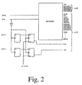
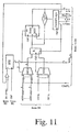
- the elementary matrix essentially consists of six main functional blocks, shown in Fig. 1.
- This circuit block receives a clock signal CkF and an 8KHz synchronization signal SYNC from the outside, from which it obtains all timing signals for the different internal functional block of the elementary matrix.
- the block can also receive two time marks from the outside M.T.1 and M.T.2 and, after synchronization of the same, they are sent during the next synchronization signal to the BP_GFU block to be inserted on all outgoing flows.
- This block essentially contains the data memory, which according to the above mentioned preferred embodiment, consists of six RAMs or RAM blocks, 1K addressing each, forming the so-called speech-memory .
- the programming of the bit-rates relevant to two adjacent flows for a maximum of 12 total programming, in the example shown, is received by the Microprocessor Interface Block BIM, described hereafter more in detail. As it shall be stated in the description, in the case of the example shown, each programming of the 32Mbit/s bit-rate is permitted only for the first of the two adjacent flows.
- Said block receives also PCM flows and relevant line synchronization signals In_Frame&Ln_Sync0, ...., In_Frame&Ln_Sync23 (Input Frame / Line Sync) required to preset the relevant channel counters, directly from the external pins of the device.
- the BP_MFE block transfers the content of cells pointed by the BP_GFU block through emission of addresses on the bus ADD, as data DATA to said BP_GFU block described below in detail.
- This block essentially contains the command memory ( command- memory ). It receives from the Microprocessor Interface Block BIM the programming of bit-rates relevant to two flows, for a maximum of 12 programming and the indication of connections to be made. Since the maximum capacity of the command memory is 4,096 cells, considering the technological restrictions mentioned above, the higher is the number of flows programmed at the maximum bit-rate, the lower is the number of flows which can be controlled.
- This block periodically measures the time phase shifting if line synchronizations Ln_Sync0, ..., LnSync23 (the relevant time position of channels having the same order number on the different flows) versus the local synchronization SYNC supplied by the BR_DT block. If a given phase shifting results changed compared to the previous scanning, communication is given to the microprocessor ⁇ P.
- the invention includes also this block which continuously and periodically checks all the connections stored in the command memory and checks the correct transfer of data from the particular incoming channel In-Frame to the outgoing channel presently selected OutFrame. If the comparison between input and output data is correct, the circuit restarts the check of the next connection; in the contrary instance it supplies the microprocessor ⁇ P with the information of the connection resulting not correct. Only after acquisition of data relevant to said information by the microprocessor, the circuit performs the check of other connections in sequence.
- This circuit block contains the control logics to dialogue with the different blocks mentioned above and can be directly connected to a commercial microprocessor ⁇ P, (for instance of the 68000 Motorola family) with data bus at 16 bits.
- ⁇ P for instance of the 68000 Motorola family
- the 8KHz synchronization signal SYNC and a clock signal CkF whose frequency F can be for instance 32 MHz, 16 Mhz or 8 MHz, are received from the outside, as shown in figure 2.
- the circuit generates and distributes the following timing signals:
- the BR_DT block can also receive, always from the outside, two time marks MT1 and MT2 (active at low level) with time not lower than 125 ⁇ and not matching the synchronization pulse.
- the presence of time marks is sampled by the clock and they are sent to the BP_GFU block where the synchronization signal inserts them in the fourth and fifth bit of the first time-slot TS0, corresponding to the first outgoing channels of the relevant output serial flow.
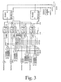
- FIG. 3 The architecture of this block is shown in detail in Fig. 3 for the first of the six 1 Kbyte memory blocks RAM1, ..., RAM6 double addressable port, WR and RD respectivelyç the scheme being recurring for the six RAMs forming the speech memory .
- Reading ports RD are controlled by the addRD address, periodically drawn by the command memory ( command memory ) of the BP_GFU block to which the information contained in the addressed cell shall be sent as described below.
- the control circuit of WR writing ports manages four flows, incoming ones for the example considered having each one a given bit-rate which can be different from the other one.
- the bit-rate programming involves two adjacent flows at the same time. Concerning each pair of flows, if the first flow is programmed at the maximum bit rate of 32Mbit/s, the second flow is automatically inhibited to the writing of the RAM memory.
- EnCkxx and EnBxx signals enable the component to operate coinciding with the relevant clock front, for the bit time and for the byte time, respectively.
- Each serial/parallel converter can consist of a register receiving on DS the serial flow and makes the channel available on the 8 bits parallel data bus DP.
- Each counter (COUNTER) associated to each input line gives the writing address of the channel to which the current information on the data bus DP belongs. Counters prepare for the use of their concerned RAM memory area according to the programmed bit-rate of the relevant input flow.
- Multiplexers MX receive all timing signals required by the BR_DT block and selecting the requested timing according to the programming received by the BIM block.
- Bistable circuits B have the function to phase shift the incoming flows at the input of the relevant converters S/P in order that these last supply data on the parallel data bus DP, in different times to enable their writing (necessarily in sequence) without requiring the use of elastic memories (writing buffers). Only the first input bistable circuit of each flow samples with the negated front of the relevant clock signal CkxF. Bistable circuits added in cascade and in gradually increased number to the first bistable sampling circuit have the scope to introduce a clock time delay on the second flow, of two clock periods on the third and of three clock periods on the fourth flow.
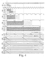
- FIG. 4 it is shown the case of four input flows reverting to the same RAM, each one programmed at a different bit-rate.
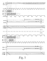
- Fig. 5 it is shown the case where the first two flows (upper part of the figure) are programmed at 16Mbit/s bit rate and the second one at 8 Mbit/s, respectively while for the other pair of flows (lower part of the figure), the first flow is programmed at 8 Mbit/s while the second one at 16Mbit/s.
- Diagrams of Fig. 5 show how writing strobes are generated, according to the programmed bit-rate. Strobes are generated every 8 bits and their time position remains rigidly bound for each flow.
- this block avails of a ( command-memory ) having a capacity of 4Kword, 16 bits, which is implemented with eight 0,5Kword RAMs.
- the reading port RD of each RAM memory block is addressed by the SFU output phase scanning (or channel) circuit which is constantly increased with the clock signal in order to address the cells of the speech-memory within a time of 125 ⁇ s of frame.
- the content of addressed cells of the speech-memory can be transmitted in any time-slot (T.S.) of one of the 24 output flows foreseen (as maximum number) in the example described.
- T.S. time-slot
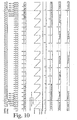
- the central band of Fig. 10 indicates the address of the command-memory cells by the scanner of outgoing phases SFU pre-set at 32 by the SYNC signal.
- the addresses of channels to transfer in time slots TS1 shall be in cells 32-:-55 for 8 Mbit/s flows, in 64-:-87 cells for 4 Mbit/s flows and in 128-:-151 cells for 2 Mbit/s flows.
- bit-rates higher than 8Mbit/s are programmed, being 4,096 the cells available in the command-memory the updating time of buffer registers (whose useful number decreases) is reduced and of course also the number of flows which can be employed.
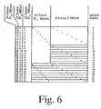
- the table shown in Fig. 6 briefly highlights the number of flows which can be employed according to the programmed bit-rate and flows repeated among them.
- said table aims at highlighting that, in the frame time of 125 ⁇ s, assuming as above that the number of cells of the command memory totals to 4096 cells, the content of 4096 channels is available at output in said frame time to control No. 8 flows at speed F. If flows are 16, the content of the same quantity of cells is available at output at a lower speed equal to F/2.
- the control diagram of the command-memory is shown in fig. 8.
- the SFU block (Outgoing Phases Scanner) can be implemented on a 12 bit MAX counter suitable to continuously read in sequence the relevant cells of the command-memory to form the different PCM flows outgoing from the switching elementary matrix.
- the counter can be preset by the synchronization signal 8khz SYNC8k at value 32, while the progress clock signal is the external clock signal applied at the CkF device.
- the IN_SYNC signal is an internal regenerated synchronization signal.
- the F&CO block implements a 12 bit MAX register/counter, where the interface block with the microprocessor writes the address of the cell to be written in the command memory, coinciding also with the Flow&Output Channel. If it is the case of an I.C.A. instruction (Adjacent Channel Instruction) then the interface block enables also a 3 bit code (PFU) to indicate the bit-rate of the concerned output flow, in such a way that the F&CO block becomes a counter which at any clock pulse increases by 8, 16, 32, 64 or 128 if the programmed bit-rate is F, F/2, F/4, F/8 or F/16 Mbit/s, respectively.
- I.C.A. instruction Adjacent Channel Instruction
- the F&CI block implements a 16/9 bit register/counter (no. 16 bits when operating as register and no.9 bits when operating as counter), where the interface deposits the information to be written in the cell identified by F&CO. If it is the case of an I.C.A. instruction then the F&CI block becomes a counter in order to increases the number of input channel to be switched.
- ⁇ C is a counter where the interface loads the number of concerned channels, in case of I.C.A. instruction only. This counter, generally locked on pace 0 keeps the counter function of F&CO and F&CI blocks locked. The interface loads all the three blocks at the same time ( ⁇ C, F&CO and F&CI) and if the ⁇ C block is loaded at a value different from 0, then F&CO and F&CI blocks progress while ⁇ C goes back up to return on pace 0.
- C1 and C2 comparators control in real time the correct operation of SFU with F&CO and of F&CI with ⁇ C, respectively.
- the ISTR signal locks the counters which are loaded with the LOAD signal at the desired value and the consequent alarms of comparators C1, C2 and C3.
- the ISTR signal is newly enabled, ⁇ C and D&CI blocks are reset and only when SFU reaches the same pace of F&CO, C1 and C2 alarms shall be newly enabled.
- the comparator C3 is used to control the drivers of the command-memory .
- drivers of port A are enabled by the E_CCM signal enabled by appropriate cyclic test.
- the F-C signal imposes complemented data at input of comparators in order to have the possibility to check the effectiveness.
- a cyclic test can enable, even in on-line operation, a check made through the BIST devices implemented for the checks generally made in the acceptance phase (incoming).
- this block performs phase shifting measurements (expressed in T.S.) between line synchronization syncX belonging to the different flows and the local synchronization IN_SYNC on which the whole operation of the implemented matrix is based.
- the address of the channel stored in the S.M. is supplied coinciding with the local synchronization IN_SYNC.
- This function enables to determine which connection has to be made to obtain the lower (or higher) switching delay.
- this block includes:
- the ⁇ P can now read the status of the scanner and the RAM output to store to which flow the phase shifting detected refers.
- the ⁇ P shall communicate to have acquired data, enabling the Phase-Rd signal, necessary to the control logic to remove the lock from the scanner, which at the next local synchronization, shall point the selection of the subsequent flow counter.
- the microprocessor can operate on this circuit through two commands:
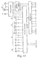
- This block implements a circuit capable to check, on line , the actual execution of connections stored in the command-memory and the correct bit-rate of input flows used.
- this control circuit is based on the content of the cells of the command-memory whose functionality is assured by the checks described above.
- each cell avails of three control bits, in addition to input channel and flow indications, namely:
- the control logic When a given cell shows the busy bit B.B., the control logic stores the content of said cell in FRAME&CHANNEL registers and its address in the INDEX register. In consideration of P32M signals coming from each circuit of the block BP_MFE, the combinatory logic prepares MX-I to select:
- the line synchronization syncX thus selected causes the reset of the TS-COUNTER and the storing of the content of channel 0 in the Tso-S/P register (more in particular only the three less significant bits defining the bit-rate received are stored).
- the control logic selects the enable-byte (EnBxe) relevant to the concerned flow and on this basis, it reconstructs the code of the bit-rate to compare with that stored in the Tso-S/P register through the CCTSo comparator.
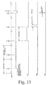
- the comparator C.I.R. hastens the control logic to enable the CP1 signal, having 125 ⁇ s duration as highlighted in the timing diagrams of Fig. 13, which enables the comparator C.TSX to identify the concerned channel and store it in the I-S/P REGISTER.
- the CP2 signal is enabled, equal to a T.S. as indicated in timing diagrams of Fig. 13, so to capture and store in O-S/P REGISTER the switched channel coming from the outgoing flow selected by MX-O controlled by the control logic.
- the time of the CP2 signal is determined by the signal EnBxu 0-:-23 representing the outgoing bit-rate set.
- control logic examines the status of comparators C.Cl-O and C.CTS o ; if their input result being equal, it waits for the third comparison of C.l.R. to enable the CP3 signal which resets the different internal circuits setting them for the re-examination of the possible presence of the B.B. in the next reading of the command memory ; on the contrary if one at least is different, the alarm is enabled, supplying the BIM block with the information of the connection being tested, the relevant contents of the three S/P registers and the code of the reconstructed bit-rate of the control logic.
- the E.C.B. bit is foreseen which can be activated by the control microprocessor when it wants and in the desired connection.
- the E.C.B. bit can be written on all the devices belonging to the same line or columns of the array. This involves and answer from all the concerned devices.
- One device only (the one relevant to the connection) shall give wrong response with byte drawn at output negated versus the one drawn at input while all the other devices signal FF for the input and 00 for the output, performing a disconnection control.
- the "in match" device (that is the one with the byte insertion) shall give wrong response with byte drawn at output and negated versus the byte inserted while all the other devices signal FF in place of the byte inserted and 00 at output.
- This block includes the signal control logic of the microprocessor, the register logic, the decoding of the operating code with relevant control and the state machine.
- this block includes:
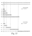
- Fig. 15 shows a timing diagram of flows incoming and outgoing from an switching matrix of the invention.
- each PCM integrated switching matrix allows, within some limits of the technological type only and which can be increased in new-generation devices, the control of input and output flows which can be programmed for different bit rates.
- this characteristic results particularly advantageous for GSM standard cellular telephone systems where, being two different operating rates foreseen (full-rate and half-rate) it is necessary to implement a switching system suitable to switch single bits instead of single bytes as it usually occurs.
- Said channel switched on an outgoing flow, it too programmed at 16 Mbit/s, is received as single bit of a 2 Mbit/s flow.
- the switching matrix shall determine a switching of the single bits instead of the single bytes as it generally occurs.
- the matrix can manage flows not time aligned among them, without employing large elastic compensation memories.
- the matrix of the invention enables to perform several connection/disconnection/insertion bytes on adjacent time slots, allowing to control the switching of a whole flow with a sole command.
Landscapes
- Engineering & Computer Science (AREA)
- Computer Networks & Wireless Communication (AREA)
- Use Of Switch Circuits For Exchanges And Methods Of Control Of Multiplex Exchanges (AREA)
- Time-Division Multiplex Systems (AREA)
Claims (9)
- Elementare PCM-Schaltmatrix für eine Anzahl N von Eingangsflüssen, welche jeweils eine Anzahl K von Kanälen enthalten, und eine Anzahl M von Ausgangsflüssen, welche jeweils eine Anzahl von H Kanälen enthalten, umfassend
Serien-Parallel-Umsetzer (S/P) für jeden der N Eingangsflüsse, wenigstens einen ersten RAM-Speicher, der als Sprachspeicher bezeichnet wird, zum Speichern von numerischen Abtastwerten der verschiedenen Kanäle der Eingangsflüsse in einer selben Anzahl von adressierbaren Abschnitten des Sprachspeichers,
wenigstens einen zweiten RAM-Speicher, der als Befehlsspeicher bezeichnet wird, zum Speichern der Verbindungskombinationen zwischen den Mehrzahlen von ankommenden und abgehenden Kanälen als Verweisadressen der relevanten Daten, welche im Sprachspeicher gespeichert sind,
einen Parallel-Serien-Umsetzer (P/S) für jeden der Ausgangsflüsse,
eine Schnittstellenschaltung (BIM) für einen Mikroprozessor zur Verbindungssteuerung,
Mittel (BCC), welche aus einer Logikschaltung, die einem externen Mikroprozessor untergeordnet ist, bestehen und die Fehlerfreiheit aller Verbindungen, welche im Befehlsspeicher gespeichert sind, und der Übertragung von Daten von einem der ankommenden Kanäle an den gegenwärtig ausgewählten abgehenden Kanal zyklisch steuern,
dadurch gekennzeichnet, dass
die Bitrate der Eingangs- und/oder Ausgangsflüsse getrennt programmiert wird und die Matrix Empfangsund Zeitgabeverteilungsmittel (BR_DT) umfasst, welche geeignet sind, ein externes Taktsignal (CFK) zu empfangen und eine Mehrzahl von Zeitgabesignalen zu erzeugen, die mit der Bitrate von Eingangs- und Ausgangsflüssen, welche durch Programmieren unabhängig auswählbar ist, im Einklang stehen;
jede Speicherstelle des Befehlsspeichers zusätzlich zu Kanal- und Eingangsflussangaben die folgenden Steuerfelder enthält:die Mittel zum Steuern der Fehlerfreiheit von Verbindungen umfassen:ein Belegtbit (B.B.), um eine Verbindung herzustellen,ein Fehlerverbindungsbit (E.C.B.), um einen Fehlzustand einer Falschverbindung zu erzwingen,ein Übertragungssteuerungsbit (L.C.B.), um die Steuerung der Bitrate des empfangenen Flusses auch während des Normalbetriebs einer bestimmten Verbindung zu ermöglichen;ein Rahmen- und Kanalregister (FRAME / CHANNEL REGISTER), welches den Inhalt einer Speicherstelle des Befehlsspeichers mit einem aktiven Belegtbit (B.B.) speichert,ein Adressregister (INDEX REGISTER) zum Speichern der Adresse einer Speicherstelle des Befehlsspeichers bei Vorhandensein eines aktiven Belegtbits (B.B.),erste Auswahlmittel (MX-I), welche dem Sprachspeicher vorgeschaltet sind und durch eine kombinatorische Logikschaltung (COMBINATORIAL LOGIC) gesteuert werden, die als Reaktion auf spezifische Signale Folgendes erzeugt:i) einen bestimmten Fluss auf einem ersten Ausgang;ii) ein bestimmtes Synchronisationssignal auf einem zweiten Ausgang;iii) eine bestimmte Sequenz von Zeittakt- und Byte-Impulsen auf einem dritten Ausgang;eine Zählschaltung (TS COUNTER), welche durch den dritten Ausgang der ersten Auswahlmittel (MX-I) zurückgestellt wird;einen ersten Serien-Parallel-Umsetzer (Tso-S/P REGISTER) zum Speichern von Bits des Zeitgabekanals 0 des Flusses, welcher dem ersten Ausgang der ersten Auswahlmittel (MX-I) entspricht;eine Steuerlogik (CONTROL LOGIC) zum Rekonstruieren eines Codes, welcher die Bitrate des ausgewählten Flusses darstellt;erste Vergleichsmittel (CCTSo) zum Vergleichen des Inhalts des ersten Serien-Parallel-Umsetzers (Tso-S/P REGISTER) mit dem rekonstruierten Code;zweite Vergleichsmittel zum Identifizieren des Kanals, welcher überprüft wird, durch Vergleichen des Inhalts der Zählschaltung (TS COUNTER) mit einem Code, der durch die kombinatorische Logikschaltung (COMBINATORIAL LOGIC) rekonstruiert wurde;einen zweiten Serien-Parallel-Umsetzer (I-S/P REGISTER) zum Speichern des Inhalts des Kanals, welcher überprüft wird, als Reaktion auf den Empfang eines Freigabesignals, das durch die zweiten Vergleichsmittel (CTSx) erzeugt wurde;zweite Auswahlmittel (MX-O), welche dem Befehlsspeicher nachgeschaltet sind, zum Verfügbarmachen des Inhalts des Kanals, welcher überprüft wird, an einem Ausgang;einen dritten Serien-Parallel-Umsetzer (O-S/P REGISTER), welcher an den Ausgang der zweiten Auswahlmittel (MX-O) angeschlossen ist;dritte Vergleichsmittel (CCI-O) zum Vergleichen des Ausgangs des dritten Serien-Parallel-Umsetzers (O-S/P REGISTER) mit dem Ausgang des zweiten Serien-Parallel-Umsetzers (I-S/P REGISTER), wobei die Steuerlogik aus dem Ausgangszustand der ersten und der dritten Vergleichsmittel (CCTSo, CCI-O) Angaben über die Fehlerfreiheit einer Verbindung erhält. - Matrix nach Anspruch 1, dadurch gekennzeichnet, dass sie Mittel zum Schreiben eines Bytes von Bits von umgekehrtem Wert in Bezug auf den Wert von übertragenen Bits in einen dritten Serien-Parallel-Umsetzer (O-S/P REGISTER) umfasst.
- Matrix nach Anspruch 1, dadurch gekennzeichnet, dass sie eine oder mehr bistabile Abtastschaltungen (B), welche in Kaskade geschaltet und in einer Anzahl sind, die für jeden Fluss der Teilanzahl von Eingangsflüssen fortlaufend zunimmt, zum Verschieben der Phasen der seriellen Eingangsflüsse untereinander und zum Erzeugen eines Synchronisationssignals (SYNCx) für einen jeweiligen programmierbaren Zähler (COUNTER) umfasst.
- Matrix nach Anspruch 1, dadurch gekennzeichnet, dass ein Schreib/Lese-Port des Befehlsspeichers mit einer Schaltung verbunden ist, welche umfasst:einen ersten Register-Zähler (F&CO), in welchen die Schnittstellenschaltung die Adresse der Stelle schreibt, die in den Befehlsspeicher zu schreiben ist, wobei der Register-Zähler einen Eingang aufweist, welcher einen Code empfängt, der die Bitrate eines jeweiligen Ausgangsflusses darstellt und die Zählerfunktion bei einer bestimmten Rate in Abhängigkeit von der Bitrate auslöst;einen zweiten Register-Zähler (F&CI), in welchen die Schnittstellenschaltung die Information schreibt, die in die Zelle zu schreiben ist, welche durch die Information identifiziert wird, die im ersten Register-Zähler (F&CO) enthalten ist, wobei solch ein Register-Zähler einen Eingang aufweist, welcher eine bestimmte Anweisung (ICA) zum Umschalten von Datenflüssen auf benachbarte Kanäle empfängt und eine Zunahme seines Inhalts feststellt;eine Zählschaltung (ΔC), in welche die Schnittstellenschaltung bei Vorhandensein der jeweiligen Anweisung (ICA) die Anzahl von Kanälen lädt, welche durch das Umschalten auf benachbarte Kanäle beteiligt sind, wobei das Vorhandensein jeglicher Anzahl in der Zählschaltung eine Verminderung ihres Inhalts und eine Zunahme des Inhalts des ersten und des zweiten Register-Zählers (F&CO, F&CI) bewirkt.
- Matrix nach Anspruch 1, dadurch gekennzeichnet, dass sie ferner umfasst:Synchronisationsmittel, welche das zuvor erwähnte interne Synchronisationssignal (IN-SYNC) zum Erzeugen von zwei Zeitmarken (M.T.1, M.T.2) verwenden, welche einen Zeitraum definieren, der nicht kürzer als der der Dauer eines Rahmens von PCM-Signalen ist;Einfügemittel der Zeitmarken in ein oder mehr Bits eines ersten Zeitschlitzes (TSO), welcher dem ersten Kanal entspricht, der aus dem relativen seriellen Ausgangsfluss kommt.
- PCM-Schaltsystem, welches eine Mehrzahl von elementaren Schaltmatrizen nach einem der Ansprüche 1 bis 5 einsetzt, die durch einen Verbindungssteuerungsmikroprozessor gesteuert werden, wobei jede elementare Matrix unter der Aufsicht des Verbindungssteuerungsmikroprozessors das Umschalten jedes einer Anzahl K von Kanälen irgendwelcher N Eingangsflüsse auf jeden der H Kanäle irgendeines von M Ausgangsflüssen einer elementaren Matrix ermöglicht, wobei die Verbindungssteuerung auf eine kontinuierliche Weise durch Vergleichen eines Bytes, das von einem bestimmten ankommenden Kanal erfasst wird, mit einem Byte, das vom entsprechenden abgehenden Kanal erfasst wird, in welchem das Byte übertragen wird, zyklisch erfolgt.
- Schaltsystem nach Anspruch 6, wobei die K Kanäle der N Eingangsflüsse nicht unbedingt auf ein lokales Synchronisationssignal abgestimmt sind, und dadurch gekennzeichnet, dass ein Kanalzähler, welcher durch ein Leitungssynchronisationssignal zurückgestellt wird, eine unabhängige Synchronisationsinformation für jeden Eingangsfluss bereitstellt.
- System nach Anspruch 6, dadurch gekennzeichnet, dass es ferner Mittel umfasst, welche Verbindungs/Trennungs-/Einfügebytes auf benachbarten Zeitschlitzen als Reaktion auf Anweisungen erzeugen, welche es ermöglichen, das Umschalten eines ganzen Flusses mit einem einzigen Befehl zu steuern.
- System nach Anspruch 6, dadurch gekennzeichnet, dass es ferner Mittel zum Einfügen von Zeitmarken für die gleichzeitige Synchronisation von fernen Empfängern auf jedem der M Ausgangsflüsse umfasst.
Applications Claiming Priority (2)
| Application Number | Priority Date | Filing Date | Title |
|---|---|---|---|
| IT95MI002161A IT1277206B1 (it) | 1995-10-20 | 1995-10-20 | Sistema di commutazione di segnali pcm impiegante una matrice con controllo automatico delle connessioni |
| ITMI952161 | 1995-10-20 |
Publications (3)
| Publication Number | Publication Date |
|---|---|
| EP0769887A2 EP0769887A2 (de) | 1997-04-23 |
| EP0769887A3 EP0769887A3 (de) | 2000-02-02 |
| EP0769887B1 true EP0769887B1 (de) | 2004-12-22 |
Family
ID=11372398
Family Applications (1)
| Application Number | Title | Priority Date | Filing Date |
|---|---|---|---|
| EP96116279A Expired - Lifetime EP0769887B1 (de) | 1995-10-20 | 1996-10-11 | PCM elementare Schaltmatrix |
Country Status (3)
| Country | Link |
|---|---|
| EP (1) | EP0769887B1 (de) |
| DE (1) | DE69634067T2 (de) |
| IT (1) | IT1277206B1 (de) |
Families Citing this family (1)
| Publication number | Priority date | Publication date | Assignee | Title |
|---|---|---|---|---|
| SE511919C2 (sv) | 1997-08-28 | 1999-12-13 | Ericsson Telefon Ab L M | En allmän väljare och ett kopplingsförfarande |
Family Cites Families (4)
| Publication number | Priority date | Publication date | Assignee | Title |
|---|---|---|---|---|
| IT1128291B (it) | 1980-05-13 | 1986-05-28 | Cselt Centro Studi Lab Telecom | Matrice elementare di commutazione pcm |
| US4485467A (en) * | 1982-02-18 | 1984-11-27 | Teknekron Infoswitch Corporation | Digital information switch matrix with on-line/off-line diagnostic features |
| IT1156368B (it) * | 1982-06-22 | 1987-02-04 | Cselt Centro Studi Lab Telecom | Rete di commutazione pcm modulare e autoinstradante per autocommutatori telefonici a comando distribuito |
| DE4117869A1 (de) * | 1991-05-31 | 1992-12-03 | Standard Elektrik Lorenz Ag | Raum- und zeit-koppelelement |
-
1995
- 1995-10-20 IT IT95MI002161A patent/IT1277206B1/it active IP Right Grant
-
1996
- 1996-10-11 DE DE69634067T patent/DE69634067T2/de not_active Expired - Lifetime
- 1996-10-11 EP EP96116279A patent/EP0769887B1/de not_active Expired - Lifetime
Also Published As
| Publication number | Publication date |
|---|---|
| ITMI952161A0 (de) | 1995-10-20 |
| EP0769887A3 (de) | 2000-02-02 |
| ITMI952161A1 (it) | 1997-04-20 |
| DE69634067D1 (de) | 2005-01-27 |
| EP0769887A2 (de) | 1997-04-23 |
| IT1277206B1 (it) | 1997-11-05 |
| DE69634067T2 (de) | 2006-01-19 |
Similar Documents
| Publication | Publication Date | Title |
|---|---|---|
| US4488290A (en) | Distributed digital exchange with improved switching system and input processor | |
| US4322843A (en) | Control information communication arrangement for a time division switching system | |
| US4173713A (en) | Continuously expandable switching network | |
| US4220823A (en) | Selectively controlled digital pad | |
| FI61375C (fi) | Foerfarande foer kontroll av genomgaoende koppling i digitala datasystem | |
| US5117417A (en) | Circuit for checking the defined transmission bit rates | |
| US4306303A (en) | Switching of digital signals | |
| US5014268A (en) | Parallel time slot interchanger matrix and switch block module for use therewith | |
| CA1171946A (en) | Time division switching matrix | |
| CA1167575A (en) | Time slot multiple circuit for the selective establishment of connections in a t.d.m. digital telecommunications system | |
| US4068098A (en) | Method of and arrangement for addressing a switch memory in a transit exchange for synchronous data signals | |
| US4685102A (en) | Switching system loopback test circuit | |
| US4035584A (en) | Space division network for time-division switching systems | |
| US4564936A (en) | Time division switching network | |
| US3984643A (en) | Method and apparatus for establishing a plurality of simultaneous conferences in a PCM switching system | |
| EP0039948B1 (de) | PCM Vermittlungselement | |
| US4581732A (en) | Time-space-time switching network using a closed-loop link | |
| CA2070000C (en) | Space/time switching element | |
| EP0769887B1 (de) | PCM elementare Schaltmatrix | |
| US5351238A (en) | Method of controlling a frame phase of a time-division switch and frame phase variable time-division switch | |
| EP0351386A1 (de) | Verfahren und Vorrichtung zur Schaltung einer Breitbandverbindung in einem digitalen Zeitschalter | |
| US5499235A (en) | Method for the simulation of transmission on a transmission network working in asynchronous transfer mode and simulator of transmission on such a network | |
| EP0769886B1 (de) | Vermittlungssystem für PCM-Signale mit einer integrierten und programmierbaren Matrix | |
| EP1104579B1 (de) | Speicherüberwachung | |
| US4060698A (en) | Digital switching center |
Legal Events
| Date | Code | Title | Description |
|---|---|---|---|
| PUAI | Public reference made under article 153(3) epc to a published international application that has entered the european phase |
Free format text: ORIGINAL CODE: 0009012 |
|
| AK | Designated contracting states |
Kind code of ref document: A2 Designated state(s): DE FR NL SE |
|
| RAP3 | Party data changed (applicant data changed or rights of an application transferred) |
Owner name: ITALTEL S.P.A. |
|
| PUAL | Search report despatched |
Free format text: ORIGINAL CODE: 0009013 |
|
| AK | Designated contracting states |
Kind code of ref document: A3 Designated state(s): DE FR NL SE |
|
| RAP1 | Party data changed (applicant data changed or rights of an application transferred) |
Owner name: ITALTEL S.P.A. |
|
| 17P | Request for examination filed |
Effective date: 20000725 |
|
| 17Q | First examination report despatched |
Effective date: 20021108 |
|
| GRAP | Despatch of communication of intention to grant a patent |
Free format text: ORIGINAL CODE: EPIDOSNIGR1 |
|
| RTI1 | Title (correction) |
Free format text: PCM ELEMENTARY SWITCHING MATRIX |
|
| GRAS | Grant fee paid |
Free format text: ORIGINAL CODE: EPIDOSNIGR3 |
|
| GRAA | (expected) grant |
Free format text: ORIGINAL CODE: 0009210 |
|
| AK | Designated contracting states |
Kind code of ref document: B1 Designated state(s): DE FR NL SE |
|
| RAP2 | Party data changed (patent owner data changed or rights of a patent transferred) |
Owner name: ITALTEL S.P.A. |
|
| REF | Corresponds to: |
Ref document number: 69634067 Country of ref document: DE Date of ref document: 20050127 Kind code of ref document: P |
|
| NLT2 | Nl: modifications (of names), taken from the european patent patent bulletin |
Owner name: ITALTEL S.P.A. |
|
| REG | Reference to a national code |
Ref country code: SE Ref legal event code: TRGR |
|
| PLBE | No opposition filed within time limit |
Free format text: ORIGINAL CODE: 0009261 |
|
| STAA | Information on the status of an ep patent application or granted ep patent |
Free format text: STATUS: NO OPPOSITION FILED WITHIN TIME LIMIT |
|
| 26N | No opposition filed |
Effective date: 20050923 |
|
| ET | Fr: translation filed | ||
| REG | Reference to a national code |
Ref country code: FR Ref legal event code: GC |
|
| REG | Reference to a national code |
Ref country code: NL Ref legal event code: PLED Effective date: 20110811 |
|
| REG | Reference to a national code |
Ref country code: FR Ref legal event code: PLFP Year of fee payment: 20 |
|
| PGFP | Annual fee paid to national office [announced via postgrant information from national office to epo] |
Ref country code: FR Payment date: 20150908 Year of fee payment: 20 |
|
| PGFP | Annual fee paid to national office [announced via postgrant information from national office to epo] |
Ref country code: DE Payment date: 20151006 Year of fee payment: 20 |
|
| PGFP | Annual fee paid to national office [announced via postgrant information from national office to epo] |
Ref country code: NL Payment date: 20151012 Year of fee payment: 20 Ref country code: SE Payment date: 20151013 Year of fee payment: 20 |
|
| REG | Reference to a national code |
Ref country code: DE Ref legal event code: R071 Ref document number: 69634067 Country of ref document: DE |
|
| REG | Reference to a national code |
Ref country code: NL Ref legal event code: MK Effective date: 20161010 |
|
| REG | Reference to a national code |
Ref country code: SE Ref legal event code: EUG |