EP0769797B1 - Magnetron - Google Patents
Magnetron Download PDFInfo
- Publication number
- EP0769797B1 EP0769797B1 EP96116635A EP96116635A EP0769797B1 EP 0769797 B1 EP0769797 B1 EP 0769797B1 EP 96116635 A EP96116635 A EP 96116635A EP 96116635 A EP96116635 A EP 96116635A EP 0769797 B1 EP0769797 B1 EP 0769797B1
- Authority
- EP
- European Patent Office
- Prior art keywords
- vanes
- cathode
- magnetron
- diameter
- unit
- Prior art date
- Legal status (The legal status is an assumption and is not a legal conclusion. Google has not performed a legal analysis and makes no representation as to the accuracy of the status listed.)
- Expired - Lifetime
Links
Images

Classifications
-
- H—ELECTRICITY
- H01—ELECTRIC ELEMENTS
- H01J—ELECTRIC DISCHARGE TUBES OR DISCHARGE LAMPS
- H01J23/00—Details of transit-time tubes of the types covered by group H01J25/00
- H01J23/36—Coupling devices having distributed capacitance and inductance, structurally associated with the tube, for introducing or removing wave energy
- H01J23/54—Filtering devices preventing unwanted frequencies or modes to be coupled to, or out of, the interaction circuit; Prevention of high frequency leakage in the environment
-
- H—ELECTRICITY
- H01—ELECTRIC ELEMENTS
- H01J—ELECTRIC DISCHARGE TUBES OR DISCHARGE LAMPS
- H01J25/00—Transit-time tubes, e.g. klystrons, travelling-wave tubes, magnetrons
- H01J25/50—Magnetrons, i.e. tubes with a magnet system producing an H-field crossing the E-field
- H01J25/52—Magnetrons, i.e. tubes with a magnet system producing an H-field crossing the E-field with an electron space having a shape that does not prevent any electron from moving completely around the cathode or guide electrode
- H01J25/58—Magnetrons, i.e. tubes with a magnet system producing an H-field crossing the E-field with an electron space having a shape that does not prevent any electron from moving completely around the cathode or guide electrode having a number of resonators; having a composite resonator, e.g. a helix
- H01J25/587—Multi-cavity magnetrons
Definitions
- the present invention relates to a magnetron according to the preamble of claim 1, and more particularly, to a magnetron which is capable of optimizing a resonance structure by changing the number of vanes, the height of vanes, an outer diameter of a cathode and a diameter of a working space.
- a conventional magnetron includes an input unit 10 having a chalk coil 12 and a condenser 14 at its lower portion, an operation unit 20 disposed on the input unit 10 and having a cathode 30, a resonance unit 40, a magnetic unit 50 and a cooling unit 60, and an output unit 70 defined on the operation unit 20.
- the cathode 30 is mounted at the central portion of the operation unit 20, and upper and lower shields 31,32 in the shape of a circular plate is mounted for preventing a deviation of electrons at the upper and lower portions of the cathode, and between the upper and lower shields 31,32 is disposed a spiral-shaped filament 33 for releasing an electron.
- the resonance unit 40 is disposed separately by a predetermined interval from an outer peripheral portion of the cathode 30.
- the magnetic unit 50 having a plurality of magnets 51 to maintain a constant magnetic field.
- a cap antenna 71 in the shape of a cap to project a microwave generated by the operation unit 20, and at an outer wall of the operation unit 20 are disposed the cooling unit 60 having a plurality of cooling pins 61 for cooling heat generated by the operation unit 20.
- an electron released from the filament 33 of the cathode 30 moves freely in a working space A except the cathode 30 in the space obtained by connecting the other end of each vane 41.
- the upper and lower shields 31,32 prevents electrons from being deviated to the upper and lower portions.
- the electrons moving freely in the working space (A) interact with the high frequency electric field formed between each vane 41 to oscillate a microwave, and the oscillated microwave is outputted through the cap antenna 71.
- the magnetron operated as described above has the international standard which was determined by International Telecommunication Union (ITU).
- the standard frequency of 2450 MHZ is distributed for a food cooker, a medical equipment and an industrial apparatus, and in a domestic microwave oven, the resonance unit 40 having ten vanes is generally adopted, and has a 700W ⁇ 1000W of a matching high frequency output.
- the output of 1250W ⁇ 1500W is employed, and twelve vanes 41 are adopted therein to enhance its output and performance, while the domestic oven adopts ten vanes, and the height of the vanes 41 is about 9mm ⁇ 10mm.
- the operating voltage is 4.3 ⁇ 4.7 kV
- the magnetic flux density of the magnetron 51 is 0,19 - 0,21 T (1900 ⁇ 2100 Gauss)
- a diameter of the filament 33 is 4.7 ⁇ 5.3mm
- a diameter of the working space (A) is 9.0 ⁇ 12.0mm.
- the magnetron 51 has a large volume and therefore an increased production cost.
- an object of the present invention to provide an improved magnetron which is capable of optimizing a resonance structure by changing the number of vanes, the height of vanes, an outer diameter of a cathode and a diameter of a working space.
- a magnetron which includes a resonance unit in which a plurality of vanes are radially disposed on an inner wall of a cylindrical anode, a cathode having a spiral filament at a central portion of the cylindrical anode, a magnetic unit having a plurality of magnets at the upper and lower portion of the resonance unit, and a cooling unit having a plurality of cooling pins at its outer portion
- the resonance unit has ten vanes having each height of 10.5mm ⁇ 12.5mm
- an outer diameter of the cathode is 4.0mm ⁇ 4.6mm
- a diameter of the working space between each symmetrical vane is 9.0mm ⁇ 12.0mm to obtain a high frequency output of 1250W ⁇ 1500W from an operating voltage of 4.3kV ⁇ 4.7kV.
- a magnetron according to the present invention has ten vanes in comparison with a conventional magnetron having twelve vanes.
- a height(V H ) of the vane is 10.5 ⁇ 12.5mm
- an outer diameter(Dc) of the cathode is 4.0 ⁇ 4.6mm
- a diameter (Da) of a working space between the vanes 41 that are symmetrical is 9.0 ⁇ 12.0mm.
- the effective surface area of the filament 33 is 200mm 2 ⁇ 260mm 2 , a magnetic flux density thereof is 18 - 20 T (1800 ⁇ 2000 Gauss), and the operating voltage thereof is 4.3 ⁇ 4.7kV identical to that of the conventional one.
- Va 300 ⁇ n ⁇ ( Ra 2 - Rc 2 )( Bg - 10600 n ⁇ )
- Va denotes an operating voltage
- Ra a radius of a working space
- Rc a radius of the cathode
- Bg a magnetic flux density
- the same output and efficiency can be achieved even when the number of the vanes is reduced to ten, the height (V H ) of the vanes 41 is 10.5 ⁇ 12.5mm, an outer diameter (Dc) of the cathode is 4.0 ⁇ 4.6mm and a diameter (Da) of the working space is 9.0 ⁇ 12.0mm.
- the present invention maintains an output of 1250 ⁇ 1500W, and the efficiency about 70 ⁇ 72% by reducing the number of the vanes and changing the height (V H ) of the vanes, an outer diameter (Dc) of the cathode, and a diameter (Da) of the working space to achieve an effect of a compactness of a product and reduction of a production cost.
Description
- The present invention relates to a magnetron according to the preamble of claim 1, and more particularly, to a magnetron which is capable of optimizing a resonance structure by changing the number of vanes, the height of vanes, an outer diameter of a cathode and a diameter of a working space.
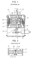
- Referring to Figures 1 through 3, a conventional magnetron includes an
input unit 10 having achalk coil 12 and acondenser 14 at its lower portion, anoperation unit 20 disposed on theinput unit 10 and having acathode 30, aresonance unit 40, amagnetic unit 50 and acooling unit 60, and anoutput unit 70 defined on theoperation unit 20. - The
cathode 30 is mounted at the central portion of theoperation unit 20, and upper andlower shields lower shields shaped filament 33 for releasing an electron. - The
resonance unit 40 is disposed separately by a predetermined interval from an outer peripheral portion of thecathode 30. There are provided twelvevanes 41, one end of which is radially disposed on an inner wall of acylindrical anode 42 and at the other end of which twostrap rings 43 in the shape of a ring are alternatively connected to the upper and lower portions of thevane 41, respectively, with a predetermined interval therebetween to form an alternate electrode. - At the upper and lower portions of the
resonance unit 40 are formed themagnetic unit 50 having a plurality ofmagnets 51 to maintain a constant magnetic field. - On the upper portion of the
operation unit 20 are provided acap antenna 71 in the shape of a cap to project a microwave generated by theoperation unit 20, and at an outer wall of theoperation unit 20 are disposed thecooling unit 60 having a plurality ofcooling pins 61 for cooling heat generated by theoperation unit 20. - The operation and disadvantages of the conventional magnetron will now be described in detail.
- First, when a constant electric field is applied between the
cathode 30 and thevane 41 through theinput unit 10 and a constant magnetic field is applied in the direction of the shaft of thecathode 30, a high frequency electric field is generated to be concentrated on the other end portion of eachvane 41. - Here, the electrical potential value of the high-frequency of each neighboring
vane 41 alternatively connected by thestrap ring 43 is reversed. - Next, an electron released from the
filament 33 of thecathode 30 moves freely in a working space A except thecathode 30 in the space obtained by connecting the other end of eachvane 41. Here, the upper andlower shields - Then, the electrons moving freely in the working space (A) interact with the high frequency electric field formed between each
vane 41 to oscillate a microwave, and the oscillated microwave is outputted through thecap antenna 71. - The magnetron operated as described above has the international standard which was determined by International Telecommunication Union (ITU). The standard frequency of 2450 MHZ is distributed for a food cooker, a medical equipment and an industrial apparatus, and in a domestic microwave oven, the
resonance unit 40 having ten vanes is generally adopted, and has a 700W∼1000W of a matching high frequency output. - Particularly, in an industrial or commercial oven, the output of 1250W∼1500W is employed, and twelve
vanes 41 are adopted therein to enhance its output and performance, while the domestic oven adopts ten vanes, and the height of thevanes 41 is about 9mm∼10mm. - Then, the operating voltage is 4.3∼4.7 kV, the magnetic flux density of the
magnetron 51 is 0,19 - 0,21 T (1900∼ 2100 Gauss), a diameter of thefilament 33 is 4.7∼5.3mm, and a diameter of the working space (A) is 9.0∼12.0mm. When themagnetron 51 is operated under the above condition, the output is maintained to be 1250∼1500W and the efficiency about 70∼72%. - However, since the industrial or commercial oven has generally twelve vanes, the
magnetron 51 has a large volume and therefore an increased production cost. - Accordingly, it is an object of the present invention to provide an improved magnetron which is capable of optimizing a resonance structure by changing the number of vanes, the height of vanes, an outer diameter of a cathode and a diameter of a working space.
- To achieve the above object, in a magnetron which includes a resonance unit in which a plurality of vanes are radially disposed on an inner wall of a cylindrical anode, a cathode having a spiral filament at a central portion of the cylindrical anode, a magnetic unit having a plurality of magnets at the upper and lower portion of the resonance unit, and a cooling unit having a plurality of cooling pins at its outer portion, the improvements are characterized in that the resonance unit has ten vanes having each height of 10.5mm∼12.5mm, an outer diameter of the cathode is 4.0mm∼4.6mm, a diameter of the working space between each symmetrical vane is 9.0mm∼12.0mm to obtain a high frequency output of 1250W∼1500W from an operating voltage of 4.3kV∼4.7kV.
- The present invention will become more fully understood from the detailed description given hereinbelow and the accompanying drawings which are given by way of illustration only, and thus are not limitative of the present invention, and wherein:
- Figure 1 is a cross-sectional view showing a conventional magnetron;
- Figure 2 is an exploded cross-sectional view showing a cathode and a resonance unit of the conventional magnetron;
- Figure 3 is a plane view showing a conventional magnetron;
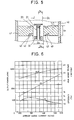
- Figure 4 is a plane view showing a magnetron according to the present invention;
- Figure 5 is a cross-sectional view showing a height of a vane of the magnetron, an outer diameter of a cathode thereof, and a diameter of a working space thereof according to the present invention; and
- Figure 6 is a graph showing an output and efficiency of the magnetron according to the present invention.
-
- As shown in Figure 4, a magnetron according to the present invention has ten vanes in comparison with a conventional magnetron having twelve vanes.
- A height(VH) of the vane is 10.5∼12.5mm, an outer diameter(Dc) of the cathode is 4.0∼4.6mm, and a diameter (Da) of a working space between the
vanes 41 that are symmetrical is 9.0∼12.0mm. - The effective surface area of the
filament 33 is 200mm2∼260mm2, a magnetic flux density thereof is 18 - 20 T (1800∼2000 Gauss), and the operating voltage thereof is 4.3∼4.7kV identical to that of the conventional one. - The description of the elements identical to the conventional ones will be omitted, and the same numeral will be put to the elements of the present invention.
- When the above conditions are adopted in the equations (1),(2) and (3)
- Here, Va denotes an operating voltage, Ra a radius of a working space, Rc a radius of the cathode, and Bg a magnetic flux density.
Ra - As shown in Figure 5, the output of 1250∼1500W is maintained and the efficiency about 70~72%.
- This means that the same output and efficiency can be achieved even when the number of the vanes is reduced to ten, the height (VH) of the
vanes 41 is 10.5∼12.5mm, an outer diameter (Dc) of the cathode is 4.0∼4.6mm and a diameter (Da) of the working space is 9.0~12.0mm. - As described above, the present invention maintains an output of 1250∼1500W, and the efficiency about 70∼72% by reducing the number of the vanes and changing the height (VH) of the vanes, an outer diameter (Dc) of the cathode, and a diameter (Da) of the working space to achieve an effect of a compactness of a product and reduction of a production cost.
- Although the preferred embodiments of the present invention have been disclosed for illustrative purposes, those skilled in the art will appreciate that various modifications, additions and substitutions are possible, without departing from the scope of the claims.
Claims (1)
- A magnetron which comprises a resonance means in which a plurality of vanes are radially disposed on an inner wall of cylindrical anode, a cathode having a spiral filament at a central portion of the cylindrical anode, a magnetic means having a plurality of magnets at the upper and lower portion of the resonance means, respectively, and a cooling means having a plurality of cooling pins around its outer wall, characterised in that the resonance means has ten vanes having each height of 10.5 mm ~ 12.5 mm, an outer diameter of the cathode is 4.0 mm ~ 4.6 mm, a diameter of the working space between each vane that is symmetrical is 9.0 mm ~12.0 mm to obtain a high frequency output of 1250W ~ 1500W from an operating voltage of 4.3kV ~ 4.7kV.
Applications Claiming Priority (2)
| Application Number | Priority Date | Filing Date | Title |
|---|---|---|---|
| KR3633895 | 1995-10-20 | ||
| KR1019950036338A KR0176847B1 (en) | 1995-10-30 | 1995-10-30 | Magnetron |
Publications (3)
| Publication Number | Publication Date |
|---|---|
| EP0769797A2 EP0769797A2 (en) | 1997-04-23 |
| EP0769797A3 EP0769797A3 (en) | 1999-02-03 |
| EP0769797B1 true EP0769797B1 (en) | 2000-05-31 |
Family
ID=19430775
Family Applications (1)
| Application Number | Title | Priority Date | Filing Date |
|---|---|---|---|
| EP96116635A Expired - Lifetime EP0769797B1 (en) | 1995-10-20 | 1996-10-17 | Magnetron |
Country Status (7)
| Country | Link |
|---|---|
| US (1) | US5798613A (en) |
| EP (1) | EP0769797B1 (en) |
| JP (1) | JP3193647B2 (en) |
| KR (1) | KR0176847B1 (en) |
| CN (1) | CN1065649C (en) |
| DE (1) | DE69608637D1 (en) |
| IN (1) | IN192336B (en) |
Families Citing this family (14)
| Publication number | Priority date | Publication date | Assignee | Title |
|---|---|---|---|---|
| EP1286379B1 (en) | 2001-08-22 | 2012-05-09 | Panasonic Corporation | Magnetron |
| KR20040013309A (en) * | 2002-08-05 | 2004-02-14 | 삼성전자주식회사 | Magnetron |
| JP4252274B2 (en) * | 2002-09-26 | 2009-04-08 | 新日本無線株式会社 | Magnetron |
| KR20040050264A (en) * | 2002-12-10 | 2004-06-16 | 삼성전자주식회사 | Magnetron, Microwave oven, and High frequency heating apparatus |
| JP4197299B2 (en) * | 2004-01-09 | 2008-12-17 | パナソニック株式会社 | Magnetron |
| KR100700554B1 (en) * | 2005-12-30 | 2007-03-28 | 엘지전자 주식회사 | Magnetron |
| EP1840933B1 (en) * | 2006-03-27 | 2012-02-15 | Panasonic Corporation | Magnetron |
| JP4503639B2 (en) * | 2007-09-11 | 2010-07-14 | 東芝ホクト電子株式会社 | Magnetron for microwave oven |
| JP5562577B2 (en) * | 2009-05-08 | 2014-07-30 | 新日本無線株式会社 | Magnetron |
| CN103280391B (en) * | 2013-05-23 | 2015-08-05 | 中国人民解放军国防科学技术大学 | Frequency-tunable axially exports relativistic magnetron |
| CN104253006B (en) * | 2013-06-27 | 2016-06-08 | 广东威特真空电子制造有限公司 | Magnetron tube core and magnetron |
| JP5805842B1 (en) * | 2014-12-03 | 2015-11-10 | 東芝ホクト電子株式会社 | Magnetron |
| CN104992892B (en) * | 2015-07-17 | 2017-01-18 | 中国工程物理研究院应用电子学研究所 | Permanent-magnet packaging relativistic magnetron |
| CN114446741B (en) * | 2021-11-18 | 2023-04-07 | 电子科技大学 | Array module magnetron and novel high-power magnetron unit |
Family Cites Families (6)
| Publication number | Priority date | Publication date | Assignee | Title |
|---|---|---|---|---|
| JP2594262B2 (en) * | 1986-10-16 | 1997-03-26 | 松下電器産業株式会社 | Magnetron |
| JPH0230036A (en) * | 1988-02-03 | 1990-01-31 | Sanyo Electric Co Ltd | Magnetron |
| KR930011063A (en) * | 1991-11-09 | 1993-06-23 | 이헌조 | magnetron |
| US5635798A (en) * | 1993-12-24 | 1997-06-03 | Hitachi, Ltd. | Magnetron with reduced dark current |
| JPH07302548A (en) * | 1994-03-09 | 1995-11-14 | Hitachi Ltd | Magnetron |
| US5635797A (en) * | 1994-03-09 | 1997-06-03 | Hitachi, Ltd. | Magnetron with improved mode separation |
-
1995
- 1995-10-30 KR KR1019950036338A patent/KR0176847B1/en not_active IP Right Cessation
-
1996
- 1996-10-14 IN IN1807CA1996 patent/IN192336B/en unknown
- 1996-10-17 EP EP96116635A patent/EP0769797B1/en not_active Expired - Lifetime
- 1996-10-17 DE DE69608637T patent/DE69608637D1/en not_active Expired - Lifetime
- 1996-10-17 US US08/734,381 patent/US5798613A/en not_active Expired - Lifetime
- 1996-10-18 JP JP27632196A patent/JP3193647B2/en not_active Expired - Fee Related
- 1996-10-18 CN CN96120163A patent/CN1065649C/en not_active Expired - Fee Related
Also Published As
| Publication number | Publication date |
|---|---|
| KR0176847B1 (en) | 1999-03-20 |
| EP0769797A2 (en) | 1997-04-23 |
| JPH09129145A (en) | 1997-05-16 |
| JP3193647B2 (en) | 2001-07-30 |
| US5798613A (en) | 1998-08-25 |
| IN192336B (en) | 2004-04-10 |
| CN1152185A (en) | 1997-06-18 |
| EP0769797A3 (en) | 1999-02-03 |
| CN1065649C (en) | 2001-05-09 |
| DE69608637D1 (en) | 2000-07-06 |
| KR970023570A (en) | 1997-05-30 |
Similar Documents
| Publication | Publication Date | Title |
|---|---|---|
| EP0769797B1 (en) | Magnetron | |
| US6653788B2 (en) | Magnetron having a lowered oscillation frequency and processing equipment employing the same | |
| US5049782A (en) | Magnetron with harmonic suppression means | |
| US5635798A (en) | Magnetron with reduced dark current | |
| US5635797A (en) | Magnetron with improved mode separation | |
| US5180946A (en) | Magnetron having coaxial choke means extending into the output side insulating tube space | |
| US4720659A (en) | Magnetron | |
| US6670762B2 (en) | Magnetron apparatus | |
| GB2601479A (en) | Magnetron | |
| US6339294B1 (en) | Magnetron anode vanes having a face portion oriented towards the anode center | |
| US7265360B2 (en) | Magnetron anode design for short wavelength operation | |
| US5537002A (en) | Frequency tunable magnetron including at least one movable backwall | |
| JPH07302548A (en) | Magnetron | |
| US5089744A (en) | Magnetron choke for microwave oven | |
| KR940009188B1 (en) | Anode structure of magnetron | |
| KR20040102844A (en) | Magnetron | |
| KR101974213B1 (en) | Magnetron for microwave oven | |
| JP2005085685A (en) | Magnetron | |
| KR19990033681A (en) | Anode assembly of magnetron | |
| KR100285851B1 (en) | Magnetron having vane structure of incline type | |
| KR200145525Y1 (en) | A permanent magnet structure of magnetron for microwave oven | |
| JPH065211A (en) | Magnetron | |
| JPH07230771A (en) | Magnetron | |
| KR200150805Y1 (en) | Magnetron | |
| JPH0652805A (en) | Magnetron |
Legal Events
| Date | Code | Title | Description |
|---|---|---|---|
| PUAI | Public reference made under article 153(3) epc to a published international application that has entered the european phase |
Free format text: ORIGINAL CODE: 0009012 |
|
| AK | Designated contracting states |
Kind code of ref document: A2 Designated state(s): DE GB IT |
|
| PUAL | Search report despatched |
Free format text: ORIGINAL CODE: 0009013 |
|
| AK | Designated contracting states |
Kind code of ref document: A3 Designated state(s): DE GB IT |
|
| 17P | Request for examination filed |
Effective date: 19990114 |
|
| GRAG | Despatch of communication of intention to grant |
Free format text: ORIGINAL CODE: EPIDOS AGRA |
|
| 17Q | First examination report despatched |
Effective date: 19990705 |
|
| GRAG | Despatch of communication of intention to grant |
Free format text: ORIGINAL CODE: EPIDOS AGRA |
|
| GRAH | Despatch of communication of intention to grant a patent |
Free format text: ORIGINAL CODE: EPIDOS IGRA |
|
| GRAH | Despatch of communication of intention to grant a patent |
Free format text: ORIGINAL CODE: EPIDOS IGRA |
|
| GRAA | (expected) grant |
Free format text: ORIGINAL CODE: 0009210 |
|
| AK | Designated contracting states |
Kind code of ref document: B1 Designated state(s): DE GB IT |
|
| PG25 | Lapsed in a contracting state [announced via postgrant information from national office to epo] |
Ref country code: IT Free format text: LAPSE BECAUSE OF FAILURE TO SUBMIT A TRANSLATION OF THE DESCRIPTION OR TO PAY THE FEE WITHIN THE PRE;WARNING: LAPSES OF ITALIAN PATENTS WITH EFFECTIVE DATE BEFORE 2007 MAY HAVE OCCURRED AT ANY TIME BEFORE 2007. THE CORRECT EFFECTIVE DATE MAY BE DIFFERENT FROM THE ONE RECORDED.SCRIBED TIME-LIMIT Effective date: 20000531 |
|
| REF | Corresponds to: |
Ref document number: 69608637 Country of ref document: DE Date of ref document: 20000706 |
|
| PG25 | Lapsed in a contracting state [announced via postgrant information from national office to epo] |
Ref country code: DE Free format text: LAPSE BECAUSE OF FAILURE TO SUBMIT A TRANSLATION OF THE DESCRIPTION OR TO PAY THE FEE WITHIN THE PRESCRIBED TIME-LIMIT Effective date: 20000901 |
|
| EN | Fr: translation not filed | ||
| PLBE | No opposition filed within time limit |
Free format text: ORIGINAL CODE: 0009261 |
|
| STAA | Information on the status of an ep patent application or granted ep patent |
Free format text: STATUS: NO OPPOSITION FILED WITHIN TIME LIMIT |
|
| 26N | No opposition filed | ||
| REG | Reference to a national code |
Ref country code: GB Ref legal event code: IF02 |
|
| PGFP | Annual fee paid to national office [announced via postgrant information from national office to epo] |
Ref country code: GB Payment date: 20081015 Year of fee payment: 13 |
|
| PG25 | Lapsed in a contracting state [announced via postgrant information from national office to epo] |
Ref country code: GB Free format text: LAPSE BECAUSE OF NON-PAYMENT OF DUE FEES Effective date: 20091017 |