EP0768761A2 - Multiple gated MOSFET for use in DC-DC converter - Google Patents
Multiple gated MOSFET for use in DC-DC converter Download PDFInfo
- Publication number
- EP0768761A2 EP0768761A2 EP96115956A EP96115956A EP0768761A2 EP 0768761 A2 EP0768761 A2 EP 0768761A2 EP 96115956 A EP96115956 A EP 96115956A EP 96115956 A EP96115956 A EP 96115956A EP 0768761 A2 EP0768761 A2 EP 0768761A2
- Authority
- EP
- European Patent Office
- Prior art keywords
- gate
- mosfet
- gates
- converter
- drain
- Prior art date
- Legal status (The legal status is an assumption and is not a legal conclusion. Google has not performed a legal analysis and makes no representation as to the accuracy of the status listed.)
- Granted
Links
- 238000010586 diagram Methods 0.000 description 11
- 238000009792 diffusion process Methods 0.000 description 9
- 239000002184 metal Substances 0.000 description 9
- 230000001360 synchronised effect Effects 0.000 description 8
- 230000000295 complement effect Effects 0.000 description 6
- 239000003990 capacitor Substances 0.000 description 4
- 239000000758 substrate Substances 0.000 description 4
- 230000001276 controlling effect Effects 0.000 description 3
- 230000001681 protective effect Effects 0.000 description 3
- 238000001228 spectrum Methods 0.000 description 3
- 230000007704 transition Effects 0.000 description 3
- 230000001419 dependent effect Effects 0.000 description 2
- 238000007599 discharging Methods 0.000 description 2
- 238000004146 energy storage Methods 0.000 description 2
- 238000000034 method Methods 0.000 description 2
- UXUFTKZYJYGMGO-CMCWBKRRSA-N (2s,3s,4r,5r)-5-[6-amino-2-[2-[4-[3-(2-aminoethylamino)-3-oxopropyl]phenyl]ethylamino]purin-9-yl]-n-ethyl-3,4-dihydroxyoxolane-2-carboxamide Chemical compound O[C@@H]1[C@H](O)[C@@H](C(=O)NCC)O[C@H]1N1C2=NC(NCCC=3C=CC(CCC(=O)NCCN)=CC=3)=NC(N)=C2N=C1 UXUFTKZYJYGMGO-CMCWBKRRSA-N 0.000 description 1
- HBBGRARXTFLTSG-UHFFFAOYSA-N Lithium ion Chemical compound [Li+] HBBGRARXTFLTSG-UHFFFAOYSA-N 0.000 description 1
- 230000015556 catabolic process Effects 0.000 description 1
- 230000001413 cellular effect Effects 0.000 description 1
- 238000006243 chemical reaction Methods 0.000 description 1
- 238000004891 communication Methods 0.000 description 1
- 230000001934 delay Effects 0.000 description 1
- 230000003111 delayed effect Effects 0.000 description 1
- 230000009977 dual effect Effects 0.000 description 1
- 230000005684 electric field Effects 0.000 description 1
- 238000005516 engineering process Methods 0.000 description 1
- 150000002500 ions Chemical class 0.000 description 1
- 229910001416 lithium ion Inorganic materials 0.000 description 1
- 239000000463 material Substances 0.000 description 1
- 238000012544 monitoring process Methods 0.000 description 1
- 238000005457 optimization Methods 0.000 description 1
- 230000003071 parasitic effect Effects 0.000 description 1
- 230000001105 regulatory effect Effects 0.000 description 1
- 229910052710 silicon Inorganic materials 0.000 description 1
- 239000010703 silicon Substances 0.000 description 1
Images


Classifications
-
- H—ELECTRICITY
- H01—ELECTRIC ELEMENTS
- H01L—SEMICONDUCTOR DEVICES NOT COVERED BY CLASS H10
- H01L29/00—Semiconductor devices adapted for rectifying, amplifying, oscillating or switching, or capacitors or resistors with at least one potential-jump barrier or surface barrier, e.g. PN junction depletion layer or carrier concentration layer; Details of semiconductor bodies or of electrodes thereof ; Multistep manufacturing processes therefor
- H01L29/66—Types of semiconductor device ; Multistep manufacturing processes therefor
- H01L29/68—Types of semiconductor device ; Multistep manufacturing processes therefor controllable by only the electric current supplied, or only the electric potential applied, to an electrode which does not carry the current to be rectified, amplified or switched
- H01L29/76—Unipolar devices, e.g. field effect transistors
- H01L29/772—Field effect transistors
- H01L29/78—Field effect transistors with field effect produced by an insulated gate
- H01L29/7833—Field effect transistors with field effect produced by an insulated gate with lightly doped drain or source extension, e.g. LDD MOSFET's; DDD MOSFET's
- H01L29/7835—Field effect transistors with field effect produced by an insulated gate with lightly doped drain or source extension, e.g. LDD MOSFET's; DDD MOSFET's with asymmetrical source and drain regions, e.g. lateral high-voltage MISFETs with drain offset region, extended drain MISFETs
-
- H—ELECTRICITY
- H01—ELECTRIC ELEMENTS
- H01L—SEMICONDUCTOR DEVICES NOT COVERED BY CLASS H10
- H01L27/00—Devices consisting of a plurality of semiconductor or other solid-state components formed in or on a common substrate
- H01L27/02—Devices consisting of a plurality of semiconductor or other solid-state components formed in or on a common substrate including semiconductor components specially adapted for rectifying, oscillating, amplifying or switching and having at least one potential-jump barrier or surface barrier; including integrated passive circuit elements with at least one potential-jump barrier or surface barrier
- H01L27/04—Devices consisting of a plurality of semiconductor or other solid-state components formed in or on a common substrate including semiconductor components specially adapted for rectifying, oscillating, amplifying or switching and having at least one potential-jump barrier or surface barrier; including integrated passive circuit elements with at least one potential-jump barrier or surface barrier the substrate being a semiconductor body
- H01L27/06—Devices consisting of a plurality of semiconductor or other solid-state components formed in or on a common substrate including semiconductor components specially adapted for rectifying, oscillating, amplifying or switching and having at least one potential-jump barrier or surface barrier; including integrated passive circuit elements with at least one potential-jump barrier or surface barrier the substrate being a semiconductor body including a plurality of individual components in a non-repetitive configuration
- H01L27/0611—Devices consisting of a plurality of semiconductor or other solid-state components formed in or on a common substrate including semiconductor components specially adapted for rectifying, oscillating, amplifying or switching and having at least one potential-jump barrier or surface barrier; including integrated passive circuit elements with at least one potential-jump barrier or surface barrier the substrate being a semiconductor body including a plurality of individual components in a non-repetitive configuration integrated circuits having a two-dimensional layout of components without a common active region
- H01L27/0617—Devices consisting of a plurality of semiconductor or other solid-state components formed in or on a common substrate including semiconductor components specially adapted for rectifying, oscillating, amplifying or switching and having at least one potential-jump barrier or surface barrier; including integrated passive circuit elements with at least one potential-jump barrier or surface barrier the substrate being a semiconductor body including a plurality of individual components in a non-repetitive configuration integrated circuits having a two-dimensional layout of components without a common active region comprising components of the field-effect type
- H01L27/0629—Devices consisting of a plurality of semiconductor or other solid-state components formed in or on a common substrate including semiconductor components specially adapted for rectifying, oscillating, amplifying or switching and having at least one potential-jump barrier or surface barrier; including integrated passive circuit elements with at least one potential-jump barrier or surface barrier the substrate being a semiconductor body including a plurality of individual components in a non-repetitive configuration integrated circuits having a two-dimensional layout of components without a common active region comprising components of the field-effect type in combination with diodes, or resistors, or capacitors
-
- H—ELECTRICITY
- H01—ELECTRIC ELEMENTS
- H01L—SEMICONDUCTOR DEVICES NOT COVERED BY CLASS H10
- H01L29/00—Semiconductor devices adapted for rectifying, amplifying, oscillating or switching, or capacitors or resistors with at least one potential-jump barrier or surface barrier, e.g. PN junction depletion layer or carrier concentration layer; Details of semiconductor bodies or of electrodes thereof ; Multistep manufacturing processes therefor
- H01L29/02—Semiconductor bodies ; Multistep manufacturing processes therefor
- H01L29/06—Semiconductor bodies ; Multistep manufacturing processes therefor characterised by their shape; characterised by the shapes, relative sizes, or dispositions of the semiconductor regions ; characterised by the concentration or distribution of impurities within semiconductor regions
- H01L29/10—Semiconductor bodies ; Multistep manufacturing processes therefor characterised by their shape; characterised by the shapes, relative sizes, or dispositions of the semiconductor regions ; characterised by the concentration or distribution of impurities within semiconductor regions with semiconductor regions connected to an electrode not carrying current to be rectified, amplified or switched and such electrode being part of a semiconductor device which comprises three or more electrodes
- H01L29/107—Substrate region of field-effect devices
- H01L29/1075—Substrate region of field-effect devices of field-effect transistors
- H01L29/1079—Substrate region of field-effect devices of field-effect transistors with insulated gate
- H01L29/1083—Substrate region of field-effect devices of field-effect transistors with insulated gate with an inactive supplementary region, e.g. for preventing punch-through, improving capacity effect or leakage current
-
- H—ELECTRICITY
- H01—ELECTRIC ELEMENTS
- H01L—SEMICONDUCTOR DEVICES NOT COVERED BY CLASS H10
- H01L29/00—Semiconductor devices adapted for rectifying, amplifying, oscillating or switching, or capacitors or resistors with at least one potential-jump barrier or surface barrier, e.g. PN junction depletion layer or carrier concentration layer; Details of semiconductor bodies or of electrodes thereof ; Multistep manufacturing processes therefor
- H01L29/66—Types of semiconductor device ; Multistep manufacturing processes therefor
- H01L29/68—Types of semiconductor device ; Multistep manufacturing processes therefor controllable by only the electric current supplied, or only the electric potential applied, to an electrode which does not carry the current to be rectified, amplified or switched
- H01L29/76—Unipolar devices, e.g. field effect transistors
- H01L29/772—Field effect transistors
- H01L29/78—Field effect transistors with field effect produced by an insulated gate
- H01L29/7801—DMOS transistors, i.e. MISFETs with a channel accommodating body or base region adjoining a drain drift region
- H01L29/7802—Vertical DMOS transistors, i.e. VDMOS transistors
- H01L29/7813—Vertical DMOS transistors, i.e. VDMOS transistors with trench gate electrode, e.g. UMOS transistors
-
- H—ELECTRICITY
- H01—ELECTRIC ELEMENTS
- H01L—SEMICONDUCTOR DEVICES NOT COVERED BY CLASS H10
- H01L29/00—Semiconductor devices adapted for rectifying, amplifying, oscillating or switching, or capacitors or resistors with at least one potential-jump barrier or surface barrier, e.g. PN junction depletion layer or carrier concentration layer; Details of semiconductor bodies or of electrodes thereof ; Multistep manufacturing processes therefor
- H01L29/66—Types of semiconductor device ; Multistep manufacturing processes therefor
- H01L29/68—Types of semiconductor device ; Multistep manufacturing processes therefor controllable by only the electric current supplied, or only the electric potential applied, to an electrode which does not carry the current to be rectified, amplified or switched
- H01L29/76—Unipolar devices, e.g. field effect transistors
- H01L29/772—Field effect transistors
- H01L29/78—Field effect transistors with field effect produced by an insulated gate
- H01L29/7831—Field effect transistors with field effect produced by an insulated gate with multiple gate structure
-
- H—ELECTRICITY
- H03—ELECTRONIC CIRCUITRY
- H03K—PULSE TECHNIQUE
- H03K17/00—Electronic switching or gating, i.e. not by contact-making and –breaking
- H03K17/12—Modifications for increasing the maximum permissible switched current
- H03K17/122—Modifications for increasing the maximum permissible switched current in field-effect transistor switches
-
- H—ELECTRICITY
- H03—ELECTRONIC CIRCUITRY
- H03K—PULSE TECHNIQUE
- H03K17/00—Electronic switching or gating, i.e. not by contact-making and –breaking
- H03K17/51—Electronic switching or gating, i.e. not by contact-making and –breaking characterised by the components used
- H03K17/56—Electronic switching or gating, i.e. not by contact-making and –breaking characterised by the components used by the use, as active elements, of semiconductor devices
- H03K17/687—Electronic switching or gating, i.e. not by contact-making and –breaking characterised by the components used by the use, as active elements, of semiconductor devices the devices being field-effect transistors
- H03K17/6871—Electronic switching or gating, i.e. not by contact-making and –breaking characterised by the components used by the use, as active elements, of semiconductor devices the devices being field-effect transistors the output circuit comprising more than one controlled field-effect transistor
- H03K17/6872—Electronic switching or gating, i.e. not by contact-making and –breaking characterised by the components used by the use, as active elements, of semiconductor devices the devices being field-effect transistors the output circuit comprising more than one controlled field-effect transistor using complementary field-effect transistors
-
- H—ELECTRICITY
- H01—ELECTRIC ELEMENTS
- H01L—SEMICONDUCTOR DEVICES NOT COVERED BY CLASS H10
- H01L29/00—Semiconductor devices adapted for rectifying, amplifying, oscillating or switching, or capacitors or resistors with at least one potential-jump barrier or surface barrier, e.g. PN junction depletion layer or carrier concentration layer; Details of semiconductor bodies or of electrodes thereof ; Multistep manufacturing processes therefor
- H01L29/02—Semiconductor bodies ; Multistep manufacturing processes therefor
- H01L29/06—Semiconductor bodies ; Multistep manufacturing processes therefor characterised by their shape; characterised by the shapes, relative sizes, or dispositions of the semiconductor regions ; characterised by the concentration or distribution of impurities within semiconductor regions
- H01L29/0684—Semiconductor bodies ; Multistep manufacturing processes therefor characterised by their shape; characterised by the shapes, relative sizes, or dispositions of the semiconductor regions ; characterised by the concentration or distribution of impurities within semiconductor regions characterised by the shape, relative sizes or dispositions of the semiconductor regions or junctions between the regions
- H01L29/0692—Surface layout
- H01L29/0696—Surface layout of cellular field-effect devices, e.g. multicellular DMOS transistors or IGBTs
-
- H—ELECTRICITY
- H01—ELECTRIC ELEMENTS
- H01L—SEMICONDUCTOR DEVICES NOT COVERED BY CLASS H10
- H01L29/00—Semiconductor devices adapted for rectifying, amplifying, oscillating or switching, or capacitors or resistors with at least one potential-jump barrier or surface barrier, e.g. PN junction depletion layer or carrier concentration layer; Details of semiconductor bodies or of electrodes thereof ; Multistep manufacturing processes therefor
- H01L29/40—Electrodes ; Multistep manufacturing processes therefor
- H01L29/41—Electrodes ; Multistep manufacturing processes therefor characterised by their shape, relative sizes or dispositions
- H01L29/423—Electrodes ; Multistep manufacturing processes therefor characterised by their shape, relative sizes or dispositions not carrying the current to be rectified, amplified or switched
- H01L29/42312—Gate electrodes for field effect devices
- H01L29/42316—Gate electrodes for field effect devices for field-effect transistors
- H01L29/4232—Gate electrodes for field effect devices for field-effect transistors with insulated gate
- H01L29/42364—Gate electrodes for field effect devices for field-effect transistors with insulated gate characterised by the insulating layer, e.g. thickness or uniformity
- H01L29/42368—Gate electrodes for field effect devices for field-effect transistors with insulated gate characterised by the insulating layer, e.g. thickness or uniformity the thickness being non-uniform
-
- H—ELECTRICITY
- H01—ELECTRIC ELEMENTS
- H01L—SEMICONDUCTOR DEVICES NOT COVERED BY CLASS H10
- H01L29/00—Semiconductor devices adapted for rectifying, amplifying, oscillating or switching, or capacitors or resistors with at least one potential-jump barrier or surface barrier, e.g. PN junction depletion layer or carrier concentration layer; Details of semiconductor bodies or of electrodes thereof ; Multistep manufacturing processes therefor
- H01L29/40—Electrodes ; Multistep manufacturing processes therefor
- H01L29/41—Electrodes ; Multistep manufacturing processes therefor characterised by their shape, relative sizes or dispositions
- H01L29/423—Electrodes ; Multistep manufacturing processes therefor characterised by their shape, relative sizes or dispositions not carrying the current to be rectified, amplified or switched
- H01L29/42312—Gate electrodes for field effect devices
- H01L29/42316—Gate electrodes for field effect devices for field-effect transistors
- H01L29/4232—Gate electrodes for field effect devices for field-effect transistors with insulated gate
- H01L29/42372—Gate electrodes for field effect devices for field-effect transistors with insulated gate characterised by the conducting layer, e.g. the length, the sectional shape or the lay-out
- H01L29/4238—Gate electrodes for field effect devices for field-effect transistors with insulated gate characterised by the conducting layer, e.g. the length, the sectional shape or the lay-out characterised by the surface lay-out
Definitions
- This invention relates to DC-DC converters and in particular to a multiple gated MOSFET that is well suited for use in DC-DC converters.
- DC-DC converters are used to convert an input DC voltage to an output DC voltage.
- the output voltage is determined by the duty cycle of a switch to which the input voltage is applied.
- FIG. 1 An example of a switching mode DC-DC converter is the complementary synchronous buck converter 10 shown in Fig. 1.
- a complementary pair of MOSFETs M1 and M2 are connected in series between the input voltage V in and ground, P-channel MOSFET M1 serving as a series switch and N-channel MOSFET M2 serving as a shunt switch.
- the common node between MOSFETs M1 and M2 is connected through a low-pass filter including an inductor L1 and a capacitor C1 which deliver the output voltage V out to the load.
- V out is fed back to a pulse width modulation (PWM) control 12, which supplies a PWM signal to the gates of MOSFETs M1 and M2.
- PWM pulse width modulation
- V out is determined by the duty cycle of the PWM signal, i.e., in this case the percentage of the time during each cycle that the PWM signal is low, thereby turning P-channel MOSFET M1 on.
- PWM control 12 is controlled by the feedback path to maintain V out at a desired level.
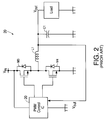
- Fig. 2 shows a totem pole N-channel synchronous buck converter 20, in which V out is determined by the duty cycle of high segment of the PWM signal applied to the gate of N-channel MOSFET M3.
- PWM control 22 supplies time delayed signals to the respective gates of MOSFETs M3 and M4 so as to prevent current "shoot through” from V in to ground.
- Fig. 3 shows a boost converter 30 which includes an N-channel MOSFET M5 and a Schottky diode 32.
- a common feature of the converters shown in Figs. 1-3, as well as numerous other converter topologies, is that one or more power MOSFET switches are used to control the transfer of energy from an energy source, here represented by V in , into at least two reactive energy storage elements, namely an inductor and a capacitor. These energy storage elements then retransfer the stored energy, when required, into the load.
- V in an energy source
- reactive energy storage elements namely an inductor and a capacitor.
- fixed frequency converters provide a predictable noise spectrum.
- a predictable noise spectrum is particularly advantageous in communication products, such as cellular phones, since shifting noise spectra can interfere with information transfer in the broadcast band.
- the energy transfer is a function of the switch on-time (or pulse width), which is modulated to compensate for an energy drain or a voltage build-up at the output of the converter.
- converters in their essential configuration, include a PWM control circuit, an inductor, a capacitor, and two MOSFET switches (or one MOSFET switch and a Schottky diode).
- every element transfers power without loss. In reality, of course, some power is lost in every element.
- the IC control circuit for example, draws power to operate internal amplifier, voltage reference, comparator, and clock circuits.
- the inductor loses power to the resistance of its coil and to the material used as its magnetic core. Even the capacitor has a series resistance component which absorbs energy.
- V in and V out affect all of the energy loss terms.
- the output capacitance term can be dominant.
- the output capacitance term is negligible. The two dominant terms are then the gate drive and conduction losses, and the power loss can be approximated by the following equation.
- P loss Q g (V gs ) ⁇ V gs ⁇ f + I 2 ⁇ R ds (V gs ) ⁇ (t on (V in )/T)
- MOSFET which provides low gate capacitive losses during light load conditions while providing low conduction losses during normal load conditions, without relying on frequency shifting or burst mode techniques.
- the MOSFET of this invention includes a single source terminal, a single drain terminal and multiple gates, each of the gates being electrically isolated from the other gate or gates and having a gate width that is different from the other gate or gates.
- the preferred embodiment has dual gates, the larger of which has a gate width which is a multiple N times the gate width of the smaller gate.
- the factor N may commonly range from 5 to 500.
- the MOSFET is preferably incorporated as a switch in a switching mode DC-DC converter.
- a PWM signal is delivered to both gates, switching the MOSFET on and off.
- the conduction losses of the converter are regulated by the total gate width of the MOSFET, which includes both gates, the larger gate carrying the major share of the current.
- the larger gate is grounded, and the PWM signal is supplied only to the smaller gate. Therefore, during a light load condition energy is not lost driving the capacitance of the larger gate.
- the output from a PWM controller is split into two paths leading to the large and small gates, respectively.
- the path leading to the large gate is ANDed with an enable signal. If the enable signal is brought high, both the large and the small gates are driven simultaneously by the PWM controller. If the enable signal is pulled low, the PWM signal to the large gate is cut off, and only the small gate is active.
- the large gate can be activated or deactivated within a single cycle of the PWM signal, making the response time of the MOSFET essentially instantaneous. This is in sharp contrast to the inherent delays in systems which rely on frequency shifting to control the power losses.
- the larger and smaller gates may be constructed in numerous ways.
- a smaller number of cells may be allocated to the smaller gate, thereby reducing the total gate "width", i.e., the combined perimeters of the cells.
- a larger number of cells are allocated to the large gate.
- the gate width may be varied by changing the cell density in certain areas of the device, with a lower cell density being used to reduce the total gate width of the small gate.
- the preferred embodiments are constructed in the form of vertical current flow MOSFETs which share common source and drain terminals.
- the multiple gate structure is applicable to MOSFETs that are vertical, lateral or quasi-lateral, with or without field oxide steps in the drain, trench gated or non-trench gated, P-channel or N-channel, double diffused or conventional, and formed in an epitaxial layer or in a diffused well.
- Fig. 1 is a circuit diagram of a conventional complementary synchronous buck converter.
- Fig. 2 is a circuit diagram of a conventional totem pole N-channel synchronous buck converter.
- Fig. 3 is a circuit diagram of a conventional boost converter.
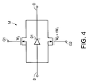
- Fig. 4 is a schematic diagram of a dual-gated N-channel MOSFET in accordance with this invention.
- Figs. 5A and 5B illustrate schematically the operation of the MOSFET of Fig. 4 in full power and light load conditions, respectively.
- Fig. 6 is a circuit diagram of an arrangement for controlling the gates of the MOSFET shown in Fig. 4.
- Fig. 7 is a circuit diagram of the inverter chain shown in Fig. 6.
- Fig. 8 illustrates schematically the capacitances present in the MOSFET of Fig. 4.
- Fig. 9 is a circuit diagram of a complementary synchronous buck converter in which an N-channel dual-gated MOSFET is used as a synchronous rectifier or shunt switch and a dual-gated P-channel MOSFET is used as a series switch.
- Fig. 10 is a circuit diagram of a buck converter in which an N-channel dual-gated MOSFET is used as a high side series switch.
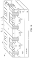
- Fig. 11 is a three-dimensional cross-sectional view of a dual-gated vertical double-diffused MOSFET (DMOS).
- DMOS dual-gated vertical double-diffused MOSFET
- Fig. 12 is a cross-sectional view of a dual-gated vertical double-diffused MOSFET in which field oxide regions are interposed between adjacent P-body diffusions.
- Fig. 13 is a three-dimensional cross-sectional view of double-diffused vertical MOSFET in which the small gate and the large gate are formed in a trench.
- Fig. 14 is a cross-sectional view of a modified version of the MOSFET shown in Fig. 13.
- Fig. 15 is a three-dimensional cross-sectional view of a dual-gated lateral N-channel MOSFET formed in a stripe pattern.
- Fig. 16 is a cross-sectional view of a square-celled version of the MOSFET shown in Fig. 15.
- Fig. 17 is a plan view of the MOSFET shown in Fig. 16.
- Fig. 18 is a cross-sectional view of a dual-gated lateral DMOSFET with field oxide regions overlying its drift regions.
- the preferred embodiment of this invention is a dual-gated power MOSFET in which the two gates are electrically isolated from each other and have substantially different gate widths.
- the MOSFET has a single drain and a single source.
- N-channel MOSFET M includes a source S and a drain D, the source S being shorted to the body of the MOSFET to prevent the parasitic NPN bipolar transistor from tuning on.
- a diode D1 represents the "antiparallel" diode formed by the PN junction between the drain D and the body of MOSFET M.
- the state of MOSFET M is controlled by gates G1 and G2, which have widths equal to W1 and W2, respectively.
- W2 is equal to the factor N times W1.
- Figs. 5A and 5B illustrate schematically the operation of MOSFET M in full power and light load conditions, respectively.
- PWM pulse width modulation
- FIG. 6 An arrangement for controlling the gates G1 and G2 is shown in Fig. 6.
- the signal from PWM control 12 is split into two paths.
- the PWM signal to the smaller gate G1 passes through inverters A1 and A2, which are sized to handle the drive requirements of gate G1 at the frequency of PWM control 12 (e.g., 1 MHz).
- inverter A2 can be stepped up in size as compared to inverter A1 so as to provide an appropriate current to gate G1.
- the signal path to gate G2 contains a similar but larger inverter chain B N which contains N inverters (see Fig. 7) to deliver a larger current to gate G2.
- gate G2 also passes through a NAND gate T, the other input to NAND gate T being connected to a source of an enable signal. If the enable signal is brought high, gate G2 will be switched in unison with gate G1. If the enable signal is pulled low, gate G2 immediately stops switching. Thus gate G2 can be enabled or disabled instantaneously, and MOSFET M therefore responds without delay to a change from a full power to a light load condition, or vice versa.
- Fig. 8 illustrates schematically the capacitances present in MOSFET M.
- C GD and C GS between gate G1 and drain D and between gate G1 and source S, respectively, and capacitances equal to N times C GD and N times C GS between gate G2 and drain D and gate G2 and source S, respectively.
- the total drain-to-source capacitance of MOSFET M is shown as (N + 1) times C DS , the drain-to - source capacitance associated with gate G1. It can be shown that the effective input capacitance and the drain current I D both are scaled down by a factor of 1/(N + 1) when gate G2 is disabled during a light load condition, while the output capacitance remains the same.
- Fig. 9 is a circuit diagram of a complementary synchronous buck converter 40 which includes the dual-gated MOSFET M as an N-channel synchronous rectifier or shunt switch.
- MOSFET M5 includes a small gate G3 and a large gate G4.
- Gates G1 and G3 are supplied in parallel by a PWM controller 42, and the PWM signal from controller 42 is directed through NAND gate T and inverter B N to gates G2 and G4.
- the output of converter 40 is fed back to controller 42 through a feedback line L2.
- Controller 42 senses a light load condition in the load and delivers a high signal on a line L3, which is connected to an input of NAND gate T. In a full power condition of the load, a low signal appears on line L3, and the PWM signal is blocked from gates G2 and G4, thereby reducing the input capacitance that must be driven by controller 42.
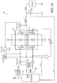
- Fig. 10 is a circuit diagram of a buck converter 50 which is similar to buck converter 40 except that an N-channel dual-gated MOSFET M6 is used as the high side series switch.
- MOSFET M6 has a small gate G5, which operates in unison with gate G1, and a large gate G6, which operates in unison with gate G2. Since the gate drive of N-channel MOSFET M6 must exceed V in , a charge pump 44 is used to supply a voltage V cp .
- Level shifters 46 and 48 are used to insure that the voltages delivered to gates G5 and G6 are referenced to the output voltage V out rather than ground.
- a make-before-break unit 49 insures that the gates of MOSFETs M and M6 are not driven high simultaneously (i.e., MOSFET M6 is turned off before MOSFET M is turned on, and vice versa), so as to prevent a shoot-through current from V in to ground.
- Figs. 11 through 18 illustrate several types of MOSFETs that can be constructed in accordance with this invention. It should be understood that the particular configurations shown in Figs. 11 through 18 are illustrative only, and that numerous other embodiments may be constructed using the principles of this invention.
- Fig. 11 is a three-dimensional cross-sectional view of a vertical double-diffused MOSFET (DMOS) 60, which is formed in an N-epitaxial (epi) layer 66. Epi layer 66 is grown on an N+ substrate 68.
- MOSFET 60 includes individual cells arrayed on the surface of epi layer 66 in a polygonal pattern. Each cell includes a P-body diffusion 62 which encloses an N+ source region 64.
- N-epi layer 66 and N+ substrate 68 form the drain of MOSFET 60, and current flow takes place in channel regions at the surface of P-body diffusions 62.
- the N+ source regions 64 and the P-body diffusions 62 are shorted together by a metal layer 65.
- the small gate (G1) of MOSFET 60 is represented as 61 and the large gate is represented as 63.
- gate 63 has a total width (approximated by the perimeters of the cells underlying gate 63) which is many times larger than the width of gate 61.
- Gates 61 and 63 are separated by a distinctive P-body diffusion 67 which does not contain a source region (and therefore carries no current) but is contacted by metal layer 65.
- Fig. 12 is a cross-sectional view of a MOSFET 70 which is similar to MOSFET 60 but in which field oxide regions 72 are interposed between adjacent P-body diffusions 62, thereby altering the structure of small gate 71 and large gate 73. Field oxide regions 72 reduce the gate-to-drain overlap capacitance and reduce the charge on gates 71 and 73.
- Fig. 13 is a three-dimensional cross-sectional view of double-diffused vertical MOSFET 80 in which the small gate 81 and the large gate 83 are formed in a trench.
- Each active cell of MOSFET 80 includes an N+ source region 84, a P-body diffusion 85 and a protective P-tub 82, which reduces the strength of the electric field at the corners of the trench and thereby prevents carrier generation and the resultant breakdown of the gate oxide layer.
- the N-epi layer 66 and N+ substrate 68 serve as the drain of the MOSFET. Current flows vertically through channel regions in the P-body diffusions adjacent the side walls of the trench.
- Small gate 81 and large gate 83 are separated by a P-tub 87 which is similar to P-tubs 82 but does not abut a source region and therefore does not carry current.
- a surface P+ region 89 overlying P-tub 87 also separates gates 81 and 83.
- Fig. 14 is a cross-sectional view of a modified version of MOSFET 80.
- MOSFET 90 there is no protective P-tub in every cell. Instead, a protective P-tub 92 is formed in only a specified percentage of the active MOSFET cells as taught in Application Serial No. 08/460,336, filed June 2, 1995, incorporated herein by reference in its entirety. This structure permits a greater cell density and reduces the on-resistance of the MOSFET.
- Fig. 14 also shows a metal layer 98 which shorts together P-tubs 87 and 92, P-body diffusions 85 and N+ source regions 84.
- Fig. 15 is a three-dimensional cross-sectional view of a lateral N-channel MOSFET 100 which is formed in a P-epi layer or P-well 102 overlying a P+ substrate 104.
- Current flows laterally near the surface of P-epi layer or P-well 102 in channel regions that are located between N+ source regions 106 and N+ drain regions 108.
- N-drift regions 107 which surround N+ drain regions 108 increase the ability of MOSFET 100 to block voltages.
- Optional P-body regions 105 may be formed around N+ source regions 106.
- a small gate 101 and a large gate 103 control current flow through the channel regions, gate 103 having a width many times the width of gate 101. Gates 101 and 103 are separated by an intervening P+ ring 109.
- MOSFET 100 is formed in a stripe pattern on the surface of P-epi or P-well 102.
- Fig. 16 is a cross-sectional view of a MOSFET 110, which is a square-celled version of MOSFET 100.
- Fig. 16 shows schematically how gates 111 and 113, N+ source regions 116, N+ drain regions 118 and P+ rings 119 are interconnected by metal layers over the surface of the silicon.
- Fig. 17 is a plan view of MOSFET 110, showing the extent of gates 111 and 113 and how interdigitated source metal lines 112 and drain metal lines 114 extend diagonally across the surface of the MOSFET in the manner taught in U.S. Patent No. 5,412,239, issued May 2, 1995. For purposes of clarity, the metal lines 112 and 114 are broken over the MOSFET cells themselves.
- Fig. 18 is a cross-sectional view of a lateral DMOSFET 120 which is formed with field oxide regions 130 overlying the N- drift regions 127.
- a small gate 121 and a large gate 123 overlap the field oxide regions 130.
- a drain metal layer 132 contacts N+ drain regions 128, and a source metal layer 134 contacts N+ source regions 126.
Landscapes
- Engineering & Computer Science (AREA)
- Power Engineering (AREA)
- Microelectronics & Electronic Packaging (AREA)
- Physics & Mathematics (AREA)
- Condensed Matter Physics & Semiconductors (AREA)
- General Physics & Mathematics (AREA)
- Computer Hardware Design (AREA)
- Ceramic Engineering (AREA)
- Dc-Dc Converters (AREA)
- Insulated Gate Type Field-Effect Transistor (AREA)
Abstract
Description
- This invention relates to DC-DC converters and in particular to a multiple gated MOSFET that is well suited for use in DC-DC converters.
- DC-DC converters are used to convert an input DC voltage to an output DC voltage. In one class of DC-DC converters, known as switching mode converters, the output voltage is determined by the duty cycle of a switch to which the input voltage is applied.
- An example of a switching mode DC-DC converter is the complementary
synchronous buck converter 10 shown in Fig. 1. A complementary pair of MOSFETs M1 and M2 are connected in series between the input voltage Vin and ground, P-channel MOSFET M1 serving as a series switch and N-channel MOSFET M2 serving as a shunt switch. The common node between MOSFETs M1 and M2 is connected through a low-pass filter including an inductor L1 and a capacitor C1 which deliver the output voltage Vout to the load. Vout is fed back to a pulse width modulation (PWM)control 12, which supplies a PWM signal to the gates of MOSFETs M1 and M2. Vout is determined by the duty cycle of the PWM signal, i.e., in this case the percentage of the time during each cycle that the PWM signal is low, thereby turning P-channel MOSFET M1 on.PWM control 12 is controlled by the feedback path to maintain Vout at a desired level. - DC-DC converters are available in a wide variety of topologies. Fig. 2 shows a totem pole N-channel
synchronous buck converter 20, in which Vout is determined by the duty cycle of high segment of the PWM signal applied to the gate of N-channel MOSFET M3. PWM control 22 supplies time delayed signals to the respective gates of MOSFETs M3 and M4 so as to prevent current "shoot through" from Vin to ground. Fig. 3 shows aboost converter 30 which includes an N-channel MOSFET M5 and a Schottkydiode 32. - A common feature of the converters shown in Figs. 1-3, as well as numerous other converter topologies, is that one or more power MOSFET switches are used to control the transfer of energy from an energy source, here represented by Vin, into at least two reactive energy storage elements, namely an inductor and a capacitor. These energy storage elements then retransfer the stored energy, when required, into the load. By monitoring Vout and by either controlling the pulse width of the signal which controls the MOSFET switches (assuming that the converter is operating at a fixed frequency), or adjusting the switching frequency (while holding the on-time of the switches constant), a constant Vout can be maintained, despite changes in Vin or the current demands of the load.
- Of the various switching mode converter topologies and control schemes, fixed frequency converters provide a predictable noise spectrum. A predictable noise spectrum is particularly advantageous in communication products, such as cellular phones, since shifting noise spectra can interfere with information transfer in the broadcast band. With a fixed clock period, the energy transfer is a function of the switch on-time (or pulse width), which is modulated to compensate for an energy drain or a voltage build-up at the output of the converter.
- Most converters, in their essential configuration, include a PWM control circuit, an inductor, a capacitor, and two MOSFET switches (or one MOSFET switch and a Schottky diode). Ideally, every element transfers power without loss. In reality, of course, some power is lost in every element. The IC control circuit, for example, draws power to operate internal amplifier, voltage reference, comparator, and clock circuits. The inductor loses power to the resistance of its coil and to the material used as its magnetic core. Even the capacitor has a series resistance component which absorbs energy.
- In practice, however, most of the power in a converter is lost in the power MOSFET that is used as the series switch and in the power MOSFET or Schottky diode that is used as the shunt switch or rectifier. These losses can be divided into four categories:
- 1. Conduction losses which arise from the MOSFETs' internal resistance, represented as I2R·D, where I is the current through the switch, R is the on-resistance of the switch, and D is the percentage of the time that the switch is on.
- 2. Gate drive losses, or the power lost charging and discharging the MOSFETs' gate capacitance, represented as

- 3. Output capacitive losses, or the power lost charging and discharging the drain capacitance of the MOSFET switch, represented as

- 4. Crossover losses, or losses which occur during the switching transitions of the MOSFETs, as a result of the simultaneous presence of a current through and a voltage across a MOSFET, represented as

- The conduction losses are strongly dependent on the current and on-resistance while the gate drive and output capacitive losses are strongly dependent on the switching frequency. At low frequencies, particularly below 100 kHz, only the conduction losses need to be considered when calculating the efficiency of the converter. At higher frequencies, particularly frequencies approaching 1 MHz, the capacitive losses become significant. Vin and Vout affect all of the energy loss terms. In high voltage converters the output capacitance term can be dominant. In low voltage applications such as computers and battery powered circuits, however, particularly those in which Vin is less than 8 volts, the output capacitance term is negligible. The two dominant terms are then the gate drive and conduction losses, and the power loss can be approximated by the following equation.

- An increase in the gate drive Vgs reduces Rds and conduction losses but increases gate drive capacitance losses. The frequency f and the load current I are weighting factors which determine which term is dominant. At higher frequencies, the gate drive capacitance loss becomes significant for all light load conditions.
- There is therefore a need for a MOSFET which provides low gate capacitive losses during light load conditions while providing low conduction losses during normal load conditions, without relying on frequency shifting or burst mode techniques.
- The MOSFET of this invention includes a single source terminal, a single drain terminal and multiple gates, each of the gates being electrically isolated from the other gate or gates and having a gate width that is different from the other gate or gates. The preferred embodiment has dual gates, the larger of which has a gate width which is a multiple N times the gate width of the smaller gate. The factor N may commonly range from 5 to 500.
- The MOSFET is preferably incorporated as a switch in a switching mode DC-DC converter. During the full power or normal running mode, a PWM signal is delivered to both gates, switching the MOSFET on and off. In this situation, the conduction losses of the converter are regulated by the total gate width of the MOSFET, which includes both gates, the larger gate carrying the major share of the current. When a light load condition is encountered, the larger gate is grounded, and the PWM signal is supplied only to the smaller gate. Therefore, during a light load condition energy is not lost driving the capacitance of the larger gate.
- In the preferred embodiment the output from a PWM controller is split into two paths leading to the large and small gates, respectively. The path leading to the large gate is ANDed with an enable signal. If the enable signal is brought high, both the large and the small gates are driven simultaneously by the PWM controller. If the enable signal is pulled low, the PWM signal to the large gate is cut off, and only the small gate is active.
- The large gate can be activated or deactivated within a single cycle of the PWM signal, making the response time of the MOSFET essentially instantaneous. This is in sharp contrast to the inherent delays in systems which rely on frequency shifting to control the power losses.
- The larger and smaller gates may be constructed in numerous ways. In a MOSFET containing a plurality of identical cells, a smaller number of cells may be allocated to the smaller gate, thereby reducing the total gate "width", i.e., the combined perimeters of the cells. A larger number of cells are allocated to the large gate. Alternatively, the gate width may be varied by changing the cell density in certain areas of the device, with a lower cell density being used to reduce the total gate width of the small gate.
- The preferred embodiments are constructed in the form of vertical current flow MOSFETs which share common source and drain terminals. However, the multiple gate structure is applicable to MOSFETs that are vertical, lateral or quasi-lateral, with or without field oxide steps in the drain, trench gated or non-trench gated, P-channel or N-channel, double diffused or conventional, and formed in an epitaxial layer or in a diffused well.
- Fig. 1 is a circuit diagram of a conventional complementary synchronous buck converter.
- Fig. 2 is a circuit diagram of a conventional totem pole N-channel synchronous buck converter.
- Fig. 3 is a circuit diagram of a conventional boost converter.
- Fig. 4 is a schematic diagram of a dual-gated N-channel MOSFET in accordance with this invention.
- Figs. 5A and 5B illustrate schematically the operation of the MOSFET of Fig. 4 in full power and light load conditions, respectively.
- Fig. 6 is a circuit diagram of an arrangement for controlling the gates of the MOSFET shown in Fig. 4.
- Fig. 7 is a circuit diagram of the inverter chain shown in Fig. 6.
- Fig. 8 illustrates schematically the capacitances present in the MOSFET of Fig. 4.
- Fig. 9 is a circuit diagram of a complementary synchronous buck converter in which an N-channel dual-gated MOSFET is used as a synchronous rectifier or shunt switch and a dual-gated P-channel MOSFET is used as a series switch.
- Fig. 10 is a circuit diagram of a buck converter in which an N-channel dual-gated MOSFET is used as a high side series switch.
- Fig. 11 is a three-dimensional cross-sectional view of a dual-gated vertical double-diffused MOSFET (DMOS).
- Fig. 12 is a cross-sectional view of a dual-gated vertical double-diffused MOSFET in which field oxide regions are interposed between adjacent P-body diffusions.
- Fig. 13 is a three-dimensional cross-sectional view of double-diffused vertical MOSFET in which the small gate and the large gate are formed in a trench.
- Fig. 14 is a cross-sectional view of a modified version of the MOSFET shown in Fig. 13.
- Fig. 15 is a three-dimensional cross-sectional view of a dual-gated lateral N-channel MOSFET formed in a stripe pattern.
- Fig. 16 is a cross-sectional view of a square-celled version of the MOSFET shown in Fig. 15.
- Fig. 17 is a plan view of the MOSFET shown in Fig. 16.
- Fig. 18 is a cross-sectional view of a dual-gated lateral DMOSFET with field oxide regions overlying its drift regions.
- The preferred embodiment of this invention is a dual-gated power MOSFET in which the two gates are electrically isolated from each other and have substantially different gate widths. The MOSFET has a single drain and a single source.
- A schematic diagram of such a MOSFET is shown in Fig. 4. N-channel MOSFET M includes a source S and a drain D, the source S being shorted to the body of the MOSFET to prevent the parasitic NPN bipolar transistor from tuning on. A diode D1 represents the "antiparallel" diode formed by the PN junction between the drain D and the body of MOSFET M. The state of MOSFET M is controlled by gates G1 and G2, which have widths equal to W1 and W2, respectively. W2 is equal to the factor N times W1.
- Figs. 5A and 5B illustrate schematically the operation of MOSFET M in full power and light load conditions, respectively. As shown in Fig. 5A, during the full power or normal running mode, both of gates G1 and G2 are switched on and off by a pulse width modulation (PWM) signal. If the multiplier factor N is large, the channel controlled by the gate G2 will carry the major share of the current, and the on-resistance of MOSFET M will be relatively low. While gate G1 could be turned off in the full power mode, it is normally convenient to continue switching it as well.
- As shown in Fig. 5B, when a light load condition is encountered, the PWM signal continues to switch gate G1 while gate G2 is grounded. Thus, during a light load condition, energy is not lost unnecessarily by driving the capacitance of the larger gate G2.
- An arrangement for controlling the gates G1 and G2 is shown in Fig. 6. The signal from
PWM control 12 is split into two paths. The PWM signal to the smaller gate G1 passes through inverters A1 and A2, which are sized to handle the drive requirements of gate G1 at the frequency of PWM control 12 (e.g., 1 MHz). If necessary, inverter A2 can be stepped up in size as compared to inverter A1 so as to provide an appropriate current to gate G1. The signal path to gate G2 contains a similar but larger inverter chain BN which contains N inverters (see Fig. 7) to deliver a larger current to gate G2. The path to gate G2 also passes through a NAND gate T, the other input to NAND gate T being connected to a source of an enable signal. If the enable signal is brought high, gate G2 will be switched in unison with gate G1. If the enable signal is pulled low, gate G2 immediately stops switching. Thus gate G2 can be enabled or disabled instantaneously, and MOSFET M therefore responds without delay to a change from a full power to a light load condition, or vice versa. - Fig. 8 illustrates schematically the capacitances present in MOSFET M. On the input side, there are capacitances CGD and CGS between gate G1 and drain D and between gate G1 and source S, respectively, and capacitances equal to N times CGD and N times CGS between gate G2 and drain D and gate G2 and source S, respectively. The total drain-to-source capacitance of MOSFET M is shown as (N + 1) times CDS, the drain-to - source capacitance associated with gate G1. It can be shown that the effective input capacitance and the drain current ID both are scaled down by a factor of 1/(N + 1) when gate G2 is disabled during a light load condition, while the output capacitance remains the same. In other words, switching from both gates G1 and G2 to gate G1 alone is not equivalent to switching to a smaller MOSFET, since certain nodes and capacitances remain in the circuit at all times. Further information concerning the operation of MOSFETs in DC-DC converters may be found in Williams et al., "High-Frequency DC/DC Converter for Lithium-Ion Battery Applications Utilizes Ultra-Fast CBiC/D Process Technology", IEEE Advan. Power Elec. Conf. (APEC), May 1995, Dallas, Texas, pp. 322-332, and Williams et al., "Optimization of Complementary Power DMOSFETs for Low-Voltage High-Frequency DC-DC Conversion", id., pp. 765-772, both of which are incorporated herein by reference in their entirety.
- Fig. 9 is a circuit diagram of a complementary
synchronous buck converter 40 which includes the dual-gated MOSFET M as an N-channel synchronous rectifier or shunt switch. A similar dual-gated P-channel MOSFET M5 is used as a series switch. MOSFET M5 includes a small gate G3 and a large gate G4. Gates G1 and G3 are supplied in parallel by aPWM controller 42, and the PWM signal fromcontroller 42 is directed through NAND gate T and inverter BN to gates G2 and G4. The output ofconverter 40 is fed back tocontroller 42 through a feedback line L2.Controller 42 senses a light load condition in the load and delivers a high signal on a line L3, which is connected to an input of NAND gate T. In a full power condition of the load, a low signal appears on line L3, and the PWM signal is blocked from gates G2 and G4, thereby reducing the input capacitance that must be driven bycontroller 42. - Fig. 10 is a circuit diagram of a
buck converter 50 which is similar to buckconverter 40 except that an N-channel dual-gated MOSFET M6 is used as the high side series switch. MOSFET M6 has a small gate G5, which operates in unison with gate G1, and a large gate G6, which operates in unison with gate G2. Since the gate drive of N-channel MOSFET M6 must exceed Vin, acharge pump 44 is used to supply a voltage Vcp. Level shifters 46 and 48 are used to insure that the voltages delivered to gates G5 and G6 are referenced to the output voltage Vout rather than ground. A make-before-break unit 49 insures that the gates of MOSFETs M and M6 are not driven high simultaneously (i.e., MOSFET M6 is turned off before MOSFET M is turned on, and vice versa), so as to prevent a shoot-through current from Vin to ground. - Figs. 11 through 18 illustrate several types of MOSFETs that can be constructed in accordance with this invention. It should be understood that the particular configurations shown in Figs. 11 through 18 are illustrative only, and that numerous other embodiments may be constructed using the principles of this invention.
- Fig. 11 is a three-dimensional cross-sectional view of a vertical double-diffused MOSFET (DMOS) 60, which is formed in an N-epitaxial (epi)
layer 66.Epi layer 66 is grown on anN+ substrate 68.MOSFET 60 includes individual cells arrayed on the surface ofepi layer 66 in a polygonal pattern. Each cell includes a P-body diffusion 62 which encloses anN+ source region 64. N-epi layer 66 andN+ substrate 68 form the drain ofMOSFET 60, and current flow takes place in channel regions at the surface of P-body diffusions 62. TheN+ source regions 64 and the P-body diffusions 62 are shorted together by ametal layer 65. - The small gate (G1) of
MOSFET 60 is represented as 61 and the large gate is represented as 63. Although not apparent from Fig. 11,gate 63 has a total width (approximated by the perimeters of the cells underlying gate 63) which is many times larger than the width ofgate 61.Gates body diffusion 67 which does not contain a source region (and therefore carries no current) but is contacted bymetal layer 65. - Fig. 12 is a cross-sectional view of a
MOSFET 70 which is similar toMOSFET 60 but in whichfield oxide regions 72 are interposed between adjacent P-body diffusions 62, thereby altering the structure ofsmall gate 71 andlarge gate 73.Field oxide regions 72 reduce the gate-to-drain overlap capacitance and reduce the charge ongates - Fig. 13 is a three-dimensional cross-sectional view of double-diffused
vertical MOSFET 80 in which thesmall gate 81 and thelarge gate 83 are formed in a trench. Each active cell ofMOSFET 80 includes anN+ source region 84, a P-body diffusion 85 and a protective P-tub 82, which reduces the strength of the electric field at the corners of the trench and thereby prevents carrier generation and the resultant breakdown of the gate oxide layer. The N-epi layer 66 andN+ substrate 68 serve as the drain of the MOSFET. Current flows vertically through channel regions in the P-body diffusions adjacent the side walls of the trench. -
Small gate 81 andlarge gate 83 are separated by a P-tub 87 which is similar to P-tubs 82 but does not abut a source region and therefore does not carry current. Asurface P+ region 89 overlying P-tub 87 also separatesgates - Fig. 14 is a cross-sectional view of a modified version of
MOSFET 80. InMOSFET 90, there is no protective P-tub in every cell. Instead, a protective P-tub 92 is formed in only a specified percentage of the active MOSFET cells as taught in Application Serial No. 08/460,336, filed June 2, 1995, incorporated herein by reference in its entirety. This structure permits a greater cell density and reduces the on-resistance of the MOSFET. Fig. 14 also shows ametal layer 98 which shorts together P-tubs body diffusions 85 andN+ source regions 84. - Fig. 15 is a three-dimensional cross-sectional view of a lateral N-
channel MOSFET 100 which is formed in a P-epi layer or P-well 102 overlying aP+ substrate 104. Current flows laterally near the surface of P-epi layer or P-well 102 in channel regions that are located betweenN+ source regions 106 andN+ drain regions 108. N-drift regions 107 which surroundN+ drain regions 108 increase the ability ofMOSFET 100 to block voltages. Optional P-body regions 105 may be formed aroundN+ source regions 106. Asmall gate 101 and alarge gate 103 control current flow through the channel regions,gate 103 having a width many times the width ofgate 101.Gates P+ ring 109. -
MOSFET 100 is formed in a stripe pattern on the surface of P-epi or P-well 102. Fig. 16 is a cross-sectional view of aMOSFET 110, which is a square-celled version ofMOSFET 100. Fig. 16 shows schematically howgates N+ source regions 116,N+ drain regions 118 and P+ rings 119 are interconnected by metal layers over the surface of the silicon. Fig. 17 is a plan view ofMOSFET 110, showing the extent ofgates source metal lines 112 and drainmetal lines 114 extend diagonally across the surface of the MOSFET in the manner taught in U.S. Patent No. 5,412,239, issued May 2, 1995. For purposes of clarity, themetal lines - Fig. 18 is a cross-sectional view of a
lateral DMOSFET 120 which is formed withfield oxide regions 130 overlying the N-drift regions 127. Asmall gate 121 and alarge gate 123 overlap thefield oxide regions 130. Adrain metal layer 132 contactsN+ drain regions 128, and asource metal layer 134 contactsN+ source regions 126. - The specific embodiments of this invention described above are intended to be illustrative only, and are not intended to limit the broad scope of this invention, which is defined in the following claims.
Claims (1)
- A multiple gated MOSFET comprising a source, a drain, a body, first and second gates, and a gate control, said first gate having a gate width that is different from a gate width of said second gate, said first gate being connected to an output terminal of said gate control, said second gate being connected to said output terminal through a switch, said first and second gates being electrically isolated from each other when said switch is open.
Applications Claiming Priority (2)
| Application Number | Priority Date | Filing Date | Title |
|---|---|---|---|
| US542611 | 1995-10-13 | ||
| US08/542,611 US5616945A (en) | 1995-10-13 | 1995-10-13 | Multiple gated MOSFET for use in DC-DC converter |
Publications (3)
| Publication Number | Publication Date |
|---|---|
| EP0768761A2 true EP0768761A2 (en) | 1997-04-16 |
| EP0768761A3 EP0768761A3 (en) | 1999-10-27 |
| EP0768761B1 EP0768761B1 (en) | 2004-12-22 |
Family
ID=24164565
Family Applications (1)
| Application Number | Title | Priority Date | Filing Date |
|---|---|---|---|
| EP96115956A Expired - Lifetime EP0768761B1 (en) | 1995-10-13 | 1996-10-04 | Multiple gated MOSFET for use in DC-DC converter |
Country Status (4)
| Country | Link |
|---|---|
| US (1) | US5616945A (en) |
| EP (1) | EP0768761B1 (en) |
| JP (1) | JP3131569B2 (en) |
| DE (1) | DE69634066T2 (en) |
Cited By (5)
| Publication number | Priority date | Publication date | Assignee | Title |
|---|---|---|---|---|
| EP1012882A1 (en) * | 1997-03-31 | 2000-06-28 | Siliconix Incorporated | Multiple gated mosfet for use in dc-dc converter |
| EP1028528A1 (en) * | 1998-08-28 | 2000-08-16 | Matsushita Electric Industrial Co., Ltd. | Switching regulator and lsi system |
| WO2002019432A2 (en) * | 2000-08-31 | 2002-03-07 | General Semiconductor, Inc. | Trench mosfet with structure having low gate charge |
| WO2004032243A1 (en) * | 2002-10-04 | 2004-04-15 | Koninklijke Philips Electronics N.V. | Power semiconductor devices |
| CN103427603A (en) * | 2012-05-22 | 2013-12-04 | 通嘉科技股份有限公司 | Extra-high-voltage assembly and method for operating extra-high-voltage assembly |
Families Citing this family (61)
| Publication number | Priority date | Publication date | Assignee | Title |
|---|---|---|---|---|
| US6184666B1 (en) * | 1998-03-09 | 2001-02-06 | 3Dlabs Inc. Ltd. | Buck converter with parallel switches |
| DE19953620A1 (en) * | 1998-11-09 | 2000-05-11 | Int Rectifier Corp | Low voltage MOS gate controlled semiconductor component, useful for a direct voltage/direct voltage converter, employs planar strip technology and has a minimal power index |
| US6168292B1 (en) * | 1998-11-10 | 2001-01-02 | Tensor Corporation | Lamp |
| US6461918B1 (en) * | 1999-12-20 | 2002-10-08 | Fairchild Semiconductor Corporation | Power MOS device with improved gate charge performance |
| JP2001251869A (en) * | 2000-03-01 | 2001-09-14 | Osaka Gas Co Ltd | Dc/ac conversion circuit, power converter and power generating system |
| JP3602028B2 (en) * | 2000-03-27 | 2004-12-15 | 沖電気工業株式会社 | Semiconductor integrated circuit |
| KR100327434B1 (en) * | 2000-05-01 | 2002-03-13 | 박종섭 | Semiconductor device |
| JP2002019558A (en) * | 2000-07-11 | 2002-01-23 | Denso Corp | Charge control circuit for capacitor, and microcomputer |
| US6696726B1 (en) * | 2000-08-16 | 2004-02-24 | Fairchild Semiconductor Corporation | Vertical MOSFET with ultra-low resistance and low gate charge |
| US7745289B2 (en) | 2000-08-16 | 2010-06-29 | Fairchild Semiconductor Corporation | Method of forming a FET having ultra-low on-resistance and low gate charge |
| US6930473B2 (en) * | 2001-08-23 | 2005-08-16 | Fairchild Semiconductor Corporation | Method and circuit for reducing losses in DC-DC converters |
| US7345342B2 (en) * | 2001-01-30 | 2008-03-18 | Fairchild Semiconductor Corporation | Power semiconductor devices and methods of manufacture |
| US6818513B2 (en) * | 2001-01-30 | 2004-11-16 | Fairchild Semiconductor Corporation | Method of forming a field effect transistor having a lateral depletion structure |
| US6803626B2 (en) * | 2002-07-18 | 2004-10-12 | Fairchild Semiconductor Corporation | Vertical charge control semiconductor device |
| US6677641B2 (en) | 2001-10-17 | 2004-01-13 | Fairchild Semiconductor Corporation | Semiconductor structure with improved smaller forward voltage loss and higher blocking capability |
| WO2002084873A1 (en) * | 2001-03-28 | 2002-10-24 | Koninklijke Philips Electronics N.V. | Synchronous rectifiers |
| DE60215391T2 (en) * | 2001-06-15 | 2007-10-25 | Apple Computer, Inc., Cupertino | ACTIVE COMPUTER HOUSING |
| KR100859701B1 (en) * | 2002-02-23 | 2008-09-23 | 페어차일드코리아반도체 주식회사 | High voltage LDMOS transistor and method for fabricating the same |
| US6784729B1 (en) * | 2002-08-14 | 2004-08-31 | Advanced Micro Devices, Inc. | Differential amplifier with input gate oxide breakdown avoidance |
| US6855985B2 (en) * | 2002-09-29 | 2005-02-15 | Advanced Analogic Technologies, Inc. | Modular bipolar-CMOS-DMOS analog integrated circuit & power transistor technology |
| US7576388B1 (en) * | 2002-10-03 | 2009-08-18 | Fairchild Semiconductor Corporation | Trench-gate LDMOS structures |
| US7652326B2 (en) * | 2003-05-20 | 2010-01-26 | Fairchild Semiconductor Corporation | Power semiconductor devices and methods of manufacture |
| KR100994719B1 (en) * | 2003-11-28 | 2010-11-16 | 페어차일드코리아반도체 주식회사 | Superjunction semiconductor device |
| US7368777B2 (en) * | 2003-12-30 | 2008-05-06 | Fairchild Semiconductor Corporation | Accumulation device with charge balance structure and method of forming the same |
| JP4610199B2 (en) * | 2004-01-14 | 2011-01-12 | ルネサスエレクトロニクス株式会社 | Semiconductor integrated circuit for DC-DC converter and DC-DC converter |
| US7352036B2 (en) | 2004-08-03 | 2008-04-01 | Fairchild Semiconductor Corporation | Semiconductor power device having a top-side drain using a sinker trench |
| US7265415B2 (en) * | 2004-10-08 | 2007-09-04 | Fairchild Semiconductor Corporation | MOS-gated transistor with reduced miller capacitance |
| TWI348262B (en) * | 2005-02-10 | 2011-09-01 | Bruno Ferrario | A circuit and method for adaptive frequency compensation for dc-to-dc converter |
| JP2008536316A (en) | 2005-04-06 | 2008-09-04 | フェアチャイルド・セミコンダクター・コーポレーション | Trench gate field effect transistor and method of forming the same |
| US7385248B2 (en) * | 2005-08-09 | 2008-06-10 | Fairchild Semiconductor Corporation | Shielded gate field effect transistor with improved inter-poly dielectric |
| US7446374B2 (en) * | 2006-03-24 | 2008-11-04 | Fairchild Semiconductor Corporation | High density trench FET with integrated Schottky diode and method of manufacture |
| US20070236518A1 (en) * | 2006-04-03 | 2007-10-11 | Oto Leonard D | Hysteretic led driver with low end linearization |
| US7319256B1 (en) | 2006-06-19 | 2008-01-15 | Fairchild Semiconductor Corporation | Shielded gate trench FET with the shield and gate electrodes being connected together |
| US8492796B2 (en) * | 2007-03-13 | 2013-07-23 | Infineon Technologies Ag | MuGFET switch |
| US8222874B2 (en) * | 2007-06-26 | 2012-07-17 | Vishay-Siliconix | Current mode boost converter using slope compensation |
| EP2208229A4 (en) | 2007-09-21 | 2011-03-16 | Fairchild Semiconductor | Superjunction structures for power devices and methods of manufacture |
| US7772668B2 (en) | 2007-12-26 | 2010-08-10 | Fairchild Semiconductor Corporation | Shielded gate trench FET with multiple channels |
| US20120273916A1 (en) | 2011-04-27 | 2012-11-01 | Yedinak Joseph A | Superjunction Structures for Power Devices and Methods of Manufacture |
| US8183892B2 (en) | 2009-06-05 | 2012-05-22 | Fairchild Semiconductor Corporation | Monolithic low impedance dual gate current sense MOSFET |
| US9263439B2 (en) | 2010-05-24 | 2016-02-16 | Infineon Technologies Americas Corp. | III-nitride switching device with an emulated diode |
| US8432000B2 (en) | 2010-06-18 | 2013-04-30 | Fairchild Semiconductor Corporation | Trench MOS barrier schottky rectifier with a planar surface using CMP techniques |
| US8674727B2 (en) | 2010-08-31 | 2014-03-18 | Infineon Technologies Austria Ag | Circuit and method for driving a transistor component based on a load condition |
| US8836028B2 (en) | 2011-04-27 | 2014-09-16 | Fairchild Semiconductor Corporation | Superjunction structures for power devices and methods of manufacture |
| US8673700B2 (en) | 2011-04-27 | 2014-03-18 | Fairchild Semiconductor Corporation | Superjunction structures for power devices and methods of manufacture |
| US8786010B2 (en) | 2011-04-27 | 2014-07-22 | Fairchild Semiconductor Corporation | Superjunction structures for power devices and methods of manufacture |
| US8772868B2 (en) | 2011-04-27 | 2014-07-08 | Fairchild Semiconductor Corporation | Superjunction structures for power devices and methods of manufacture |
| US8698229B2 (en) * | 2011-05-31 | 2014-04-15 | Infineon Technologies Austria Ag | Transistor with controllable compensation regions |
| US9166028B2 (en) * | 2011-05-31 | 2015-10-20 | Infineon Technologies Austria Ag | Circuit configured to adjust the activation state of transistors based on load conditions |
| US8803205B2 (en) | 2011-05-31 | 2014-08-12 | Infineon Technologies Austria Ag | Transistor with controllable compensation regions |
| WO2013032906A1 (en) * | 2011-08-29 | 2013-03-07 | Efficient Power Conversion Corporation | Parallel connection methods for high performance transistors |
| JP6106045B2 (en) * | 2013-03-22 | 2017-03-29 | 株式会社東芝 | Light receiving circuit |
| JP6088331B2 (en) | 2013-04-10 | 2017-03-01 | 富士通株式会社 | Charge / discharge signal circuit and DCDC converter |
| JP6171861B2 (en) | 2013-11-07 | 2017-08-02 | 富士通株式会社 | Charge / discharge signal circuit and DCDC converter |
| JP2015135927A (en) * | 2014-01-20 | 2015-07-27 | 株式会社東芝 | Semiconductor device, semiconductor module and electronic circuit |
| DE102015112502B4 (en) | 2015-07-30 | 2021-11-04 | Infineon Technologies Ag | Semiconductor components |
| US9882492B2 (en) | 2015-12-08 | 2018-01-30 | Infineon Technologies Austria Ag | Control of asymmetric parallel synchronous rectifiers in power converter topologies |
| JP6289600B2 (en) * | 2016-12-22 | 2018-03-07 | 三菱電機株式会社 | Semiconductor device |
| US10003337B1 (en) * | 2017-05-17 | 2018-06-19 | International Business Machines Corporation | Resonant virtual supply booster for synchronous logic circuits and other circuits with use of on-chip integrated magnetic inductor |
| US10992221B2 (en) * | 2018-04-09 | 2021-04-27 | Semiconductor Components Industries, Llc | Efficient buck-boost charge pump and method therefor |
| US10748891B1 (en) * | 2019-02-12 | 2020-08-18 | Qualcomm Incorporated | Electrostatic discharge (ESD) robust transistor |
| JP7293757B2 (en) * | 2019-03-15 | 2023-06-20 | 株式会社村田製作所 | Switch circuit, high frequency module and communication device |
Citations (3)
| Publication number | Priority date | Publication date | Assignee | Title |
|---|---|---|---|---|
| US4841165A (en) * | 1988-02-12 | 1989-06-20 | Wesley H. Heinmiller | D. C. power controller |
| EP0330142A2 (en) * | 1988-02-22 | 1989-08-30 | Kabushiki Kaisha Toshiba | Multi-gate field-effect transistor |
| US5243234A (en) * | 1991-03-20 | 1993-09-07 | Industrial Technology Research Institute | Dual gate LDMOSFET device for reducing on state resistance |
Family Cites Families (3)
| Publication number | Priority date | Publication date | Assignee | Title |
|---|---|---|---|---|
| US3660697A (en) * | 1970-02-16 | 1972-05-02 | Bell Telephone Labor Inc | Monolithic semiconductor apparatus adapted for sequential charge transfer |
| EP0051693B1 (en) * | 1980-11-12 | 1985-06-19 | Ibm Deutschland Gmbh | Electrically switchable read-only memory |
| JPH0338878A (en) * | 1989-07-05 | 1991-02-19 | Nec Corp | Dual gate type insulated gate field effect transistor |
-
1995
- 1995-10-13 US US08/542,611 patent/US5616945A/en not_active Expired - Lifetime
-
1996
- 1996-10-04 EP EP96115956A patent/EP0768761B1/en not_active Expired - Lifetime
- 1996-10-04 DE DE69634066T patent/DE69634066T2/en not_active Expired - Lifetime
- 1996-10-09 JP JP08287598A patent/JP3131569B2/en not_active Expired - Fee Related
Patent Citations (3)
| Publication number | Priority date | Publication date | Assignee | Title |
|---|---|---|---|---|
| US4841165A (en) * | 1988-02-12 | 1989-06-20 | Wesley H. Heinmiller | D. C. power controller |
| EP0330142A2 (en) * | 1988-02-22 | 1989-08-30 | Kabushiki Kaisha Toshiba | Multi-gate field-effect transistor |
| US5243234A (en) * | 1991-03-20 | 1993-09-07 | Industrial Technology Research Institute | Dual gate LDMOSFET device for reducing on state resistance |
Non-Patent Citations (3)
| Title |
|---|
| PATENT ABSTRACTS OF JAPAN vol. 015, no. 175 (E-1063), 2 May 1991 (1991-05-02) & JP 03 038878 A (NEC CORP), 19 February 1991 (1991-02-19) * |
| WILLIAMS R K ET AL: "HIGH-FREQUENCY DC/DC CONVERTER FOR LITHIUM-ION BATTERY APPLICATIONSUTILIZES ULTRA-FAST CBIC/D PROCESS TECHNOLOGY" PROCEEDINGS OF THE ANNUAL APPLED POWER ELECTRONICS CONFERENCE AND EXPOSITION. (APEC), DALLAS, MAR. 5 - 9, 1995, vol. 1, no. CONF. 10, 5 March 1995 (1995-03-05), pages 322-332, XP000528150 INSTITUTE OF ELECTRICAL AND ELECTRONICS ENGINEERSISBN: 0-7803-2483-8 * |
| WILLIAMS R K ET AL: "OPTIMIZATION OF COMPLEMENTARY POWER DMOSFETS FOR LOW-VOLTAGE HIGH- FREQUENCY DC-DC CONVERSION" PROCEEDINGS OF THE ANNUAL APPLED POWER ELECTRONICS CONFERENCE AND EXPOSITION (APEX), DALLAS, MAR. 5 - 9, 1995, vol. 2, no. CONF. 10, 5 March 1995 (1995-03-05), pages 765-772, XP000528092 INSTITUTE OF ELECTRICAL AND ELECTRONICS ENGINEERSISBN: 0-7803-2483-8 * |
Cited By (12)
| Publication number | Priority date | Publication date | Assignee | Title |
|---|---|---|---|---|
| EP1012882A1 (en) * | 1997-03-31 | 2000-06-28 | Siliconix Incorporated | Multiple gated mosfet for use in dc-dc converter |
| EP1012882A4 (en) * | 1997-03-31 | 2004-08-11 | Siliconix Inc | Multiple gated mosfet for use in dc-dc converter |
| EP1028528A1 (en) * | 1998-08-28 | 2000-08-16 | Matsushita Electric Industrial Co., Ltd. | Switching regulator and lsi system |
| EP1028528A4 (en) * | 1998-08-28 | 2001-10-10 | Matsushita Electric Ind Co Ltd | Switching regulator and lsi system |
| US6429633B1 (en) | 1998-08-28 | 2002-08-06 | Matsushita Electric Industrial Co., Ltd. | Switching regulator and LSI system |
| WO2002019432A2 (en) * | 2000-08-31 | 2002-03-07 | General Semiconductor, Inc. | Trench mosfet with structure having low gate charge |
| WO2002019432A3 (en) * | 2000-08-31 | 2003-03-06 | Gen Semiconductor Inc | Trench mosfet with structure having low gate charge |
| US6713352B2 (en) | 2000-08-31 | 2004-03-30 | General Semiconductor, Inc. | Method of forming a trench MOSFET with structure having increased cell density and low gate charge |
| KR100759939B1 (en) * | 2000-08-31 | 2007-09-21 | 제네럴 세미컨덕터, 인코포레이티드 | A trench mosfet device and method of forming the same |
| WO2004032243A1 (en) * | 2002-10-04 | 2004-04-15 | Koninklijke Philips Electronics N.V. | Power semiconductor devices |
| CN103427603A (en) * | 2012-05-22 | 2013-12-04 | 通嘉科技股份有限公司 | Extra-high-voltage assembly and method for operating extra-high-voltage assembly |
| CN103427603B (en) * | 2012-05-22 | 2016-09-21 | 通嘉科技股份有限公司 | Supertension assembly and the method operating supertension assembly |
Also Published As
| Publication number | Publication date |
|---|---|
| DE69634066D1 (en) | 2005-01-27 |
| JPH09223799A (en) | 1997-08-26 |
| US5616945A (en) | 1997-04-01 |
| JP3131569B2 (en) | 2001-02-05 |
| EP0768761B1 (en) | 2004-12-22 |
| EP0768761A3 (en) | 1999-10-27 |
| DE69634066T2 (en) | 2005-12-15 |
Similar Documents
| Publication | Publication Date | Title |
|---|---|---|
| US5616945A (en) | Multiple gated MOSFET for use in DC-DC converter | |
| US5973367A (en) | Multiple gated MOSFET for use in DC-DC converter | |
| US11671004B2 (en) | Power converter with multi-level topology | |
| US20080203991A1 (en) | DC-DC Converter that Includes a High Frequency Power MESFET Gate Drive Circuit | |
| US20080191679A1 (en) | High-Frequency Buck Converter that Includes a Cascode MESFET-MOSFET Power Switch | |
| US20080186004A1 (en) | High-Frequency Power MESFET Boost Switching Power Supply | |
| US9331576B2 (en) | Multiple output dual-polarity boost converter | |
| USRE40352E1 (en) | Switch mode power supply with reduced switching losses | |
| TWI406484B (en) | Time-multiplexed multi-output dc/dc converters and voltage regulators | |
| US7564704B2 (en) | Method of forming a power supply controller and structure therefor | |
| US9401644B2 (en) | Trench MOSFET having an independent coupled element in a trench | |
| CN1602579A (en) | Flyback power converter | |
| US20030111983A1 (en) | Efficient buck topology DC-DC power stage utilizing monolithic N- channel upper FET and pilot current sensing | |
| US7915879B2 (en) | Switching converter including a rectifier element with nonlinear capacitance | |
| CN111211087A (en) | Power semiconductor transistor with improved gate charge | |
| CN104221209A (en) | Photovoltaic system charge controller having buck converter with reversed MOSFETs | |
| EP3935737A1 (en) | Transistor arrangement and electronic circuit with a transistor arrangement | |
| US20130135904A1 (en) | Converter circuit | |
| US7038295B2 (en) | DC/DC converter with depletion mode compound semiconductor field effect transistor switching device | |
| JPH0698540A (en) | Synchronous rectifier circuit | |
| CN101009463A (en) | Zero voltage switching in a power converter | |
| WO2006038201A2 (en) | Power semiconductor device and corresponding circuit | |
| JPH02256191A (en) | El luminous power circuit | |
| KR20010009962A (en) | Soft switching power converter having distributed transformers and distributed power switches of parallel structure |
Legal Events
| Date | Code | Title | Description |
|---|---|---|---|
| PUAI | Public reference made under article 153(3) epc to a published international application that has entered the european phase |
Free format text: ORIGINAL CODE: 0009012 |
|
| AK | Designated contracting states |
Kind code of ref document: A2 Designated state(s): DE FR GB IT NL SE |
|
| PUAL | Search report despatched |
Free format text: ORIGINAL CODE: 0009013 |
|
| AK | Designated contracting states |
Kind code of ref document: A3 Designated state(s): DE FR GB IT NL SE |
|
| RIC1 | Information provided on ipc code assigned before grant |
Free format text: 6H 03K 17/687 A, 6H 03K 17/12 B |
|
| 17P | Request for examination filed |
Effective date: 20000419 |
|
| GRAP | Despatch of communication of intention to grant a patent |
Free format text: ORIGINAL CODE: EPIDOSNIGR1 |
|
| GRAS | Grant fee paid |
Free format text: ORIGINAL CODE: EPIDOSNIGR3 |
|
| GRAA | (expected) grant |
Free format text: ORIGINAL CODE: 0009210 |
|
| AK | Designated contracting states |
Kind code of ref document: B1 Designated state(s): DE FR GB IT NL SE |
|
| PG25 | Lapsed in a contracting state [announced via postgrant information from national office to epo] |
Ref country code: NL Free format text: LAPSE BECAUSE OF FAILURE TO SUBMIT A TRANSLATION OF THE DESCRIPTION OR TO PAY THE FEE WITHIN THE PRESCRIBED TIME-LIMIT Effective date: 20041222 Ref country code: IT Free format text: LAPSE BECAUSE OF FAILURE TO SUBMIT A TRANSLATION OF THE DESCRIPTION OR TO PAY THE FEE WITHIN THE PRE;WARNING: LAPSES OF ITALIAN PATENTS WITH EFFECTIVE DATE BEFORE 2007 MAY HAVE OCCURRED AT ANY TIME BEFORE 2007. THE CORRECT EFFECTIVE DATE MAY BE DIFFERENT FROM THE ONE RECORDED.SCRIBED TIME-LIMIT Effective date: 20041222 Ref country code: FR Free format text: LAPSE BECAUSE OF FAILURE TO SUBMIT A TRANSLATION OF THE DESCRIPTION OR TO PAY THE FEE WITHIN THE PRESCRIBED TIME-LIMIT Effective date: 20041222 |
|
| REG | Reference to a national code |
Ref country code: GB Ref legal event code: FG4D |
|
| REF | Corresponds to: |
Ref document number: 69634066 Country of ref document: DE Date of ref document: 20050127 Kind code of ref document: P |
|
| PG25 | Lapsed in a contracting state [announced via postgrant information from national office to epo] |
Ref country code: SE Free format text: LAPSE BECAUSE OF FAILURE TO SUBMIT A TRANSLATION OF THE DESCRIPTION OR TO PAY THE FEE WITHIN THE PRESCRIBED TIME-LIMIT Effective date: 20050322 |
|
| NLV1 | Nl: lapsed or annulled due to failure to fulfill the requirements of art. 29p and 29m of the patents act | ||
| PG25 | Lapsed in a contracting state [announced via postgrant information from national office to epo] |
Ref country code: GB Free format text: LAPSE BECAUSE OF NON-PAYMENT OF DUE FEES Effective date: 20051004 |
|
| PLBE | No opposition filed within time limit |
Free format text: ORIGINAL CODE: 0009261 |
|
| STAA | Information on the status of an ep patent application or granted ep patent |
Free format text: STATUS: NO OPPOSITION FILED WITHIN TIME LIMIT |
|
| 26N | No opposition filed |
Effective date: 20050923 |
|
| EN | Fr: translation not filed | ||
| GBPC | Gb: european patent ceased through non-payment of renewal fee |
Effective date: 20051004 |
|
| PGFP | Annual fee paid to national office [announced via postgrant information from national office to epo] |
Ref country code: DE Payment date: 20141029 Year of fee payment: 19 |
|
| REG | Reference to a national code |
Ref country code: DE Ref legal event code: R119 Ref document number: 69634066 Country of ref document: DE |
|
| PG25 | Lapsed in a contracting state [announced via postgrant information from national office to epo] |
Ref country code: DE Free format text: LAPSE BECAUSE OF NON-PAYMENT OF DUE FEES Effective date: 20160503 |