EP0767480A2 - Wendeltyp-Wanderfeldröhre - Google Patents
Wendeltyp-Wanderfeldröhre Download PDFInfo
- Publication number
- EP0767480A2 EP0767480A2 EP96115837A EP96115837A EP0767480A2 EP 0767480 A2 EP0767480 A2 EP 0767480A2 EP 96115837 A EP96115837 A EP 96115837A EP 96115837 A EP96115837 A EP 96115837A EP 0767480 A2 EP0767480 A2 EP 0767480A2
- Authority
- EP
- European Patent Office
- Prior art keywords
- circuit period
- circuit
- velocity
- helix
- uniform
- Prior art date
- Legal status (The legal status is an assumption and is not a legal conclusion. Google has not performed a legal analysis and makes no representation as to the accuracy of the status listed.)
- Withdrawn
Links
Images


Classifications
-
- H—ELECTRICITY
- H01—ELECTRIC ELEMENTS
- H01J—ELECTRIC DISCHARGE TUBES OR DISCHARGE LAMPS
- H01J23/00—Details of transit-time tubes of the types covered by group H01J25/00
- H01J23/16—Circuit elements, having distributed capacitance and inductance, structurally associated with the tube and interacting with the discharge
- H01J23/24—Slow-wave structures, e.g. delay systems
- H01J23/26—Helical slow-wave structures; Adjustment therefor
Definitions
- the present invention relates to a helix travelling-wave (TW) tube and, more particularly, to a helix TW tube having a helix wave delay circuit for improving a beam efficiency and reducing backward wave oscillation.
- TW travelling-wave
- a helix TW tube has an electron gun for emitting an electron beam, a helix wave delay circuit for causing the electron beam and high frequency to interact with each other, a high frequency input section for inputting the high frequency to the wave delay circuit, a high frequency output section for outputting the high frequency, and a magnetic field device for causing the electron beam to converge to a preselected diameter during propagation through the wave delay circuit.
- a magnetic field device for the interaction between the electron beam and the high frequency, it is necessary that electrons has a velocity substantially equal to the phase velocity of the high frequency.
- the helix wave delay circuit allows the high frequency to propagate along its helix at the velocity of light.
- the delay circuit allows the high frequency to propagate at a speed P/2a ⁇ times the velocity of light in the axial direction of the helix which is parallel to the direction of propagation of the electron beam.
- the high frequency forms an electric field on the helix, so that the electron beam input to the delay circuit is decelerated or accelerated.
- circuit period refer to the period of the helix and is sometimes referred to as a helix pitch.
- the velocity of the electron beam and the phase velocity of the high frequency do not interact with each other, so that amplification is not effected.
- the velocity of the electron beam is selected to be slightly greater than the phase velocity of the high frequency, a dense group of electrons concentrate on the deceleration region of the high frequency electric field formed on the helix. In the deceleration region, the electrons are decelerated with the result that a difference in kinetic energy between the initial velocity and the lowered velocity is transformed to the energy of the high frequency.
- the high frequency electric field on the helix is intensified, and in turn promotes the velocity modulation of the electrons.
- the electric field is further intensified. Because such interaction occurs continuously as the electron beam and high frequency advance, the energy of the high frequency sequentially increases toward the output end of the helix, i.e., the high frequency is amplified.
- the TW tube or high frequency amplifier amplifies given high frequency input power. So long as the high frequency input power is small, the output voltage of the tube is proportional to the input power. The operation to occur in this range is referred to as a small signal operation. When the input power exceeds the above range, the tube operates nonlinearly and in due cause reaches its limit output (saturation output). This is referred to as a great signal operation. In this respect, the conventional TW tube with the velocity taper has the following problems.
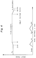
- the helix wave delay circuit has a uniform circuit period P0 portion having a uniform circuit period P0, a velocity taper portion where a circuit period varies from P0 to P1, a uniform circuit period P1 portion having a uniform circuit period P1 greater than P0, a velocity taper portion where the circuit period varies from P1 to P2, and a uniform circuit period P2 portion having a uniform circuit period P2 smaller than P1, as named from the side adjoining the high frequency input section.
- a difference ⁇ B between the two velocity coefficients B is selected to lie in a range of: 1.95 ⁇ ⁇ B ⁇ 2.1
- the uniform circuit period P0 portion and uniform circuit period P1 portion each has a particular length selected such that a small signal gain becomes maximum at a voltage satisfying the Eqs. (1)-(3).
- the TW tube has an electron gun 2, a collector 3, a wave attenuator (high frequency attenuator) 4, a wave input section (high frequency input section) 5, a wave output section (high frequency output section) 6, and a helix wave delay circuit 7.
- the wave input section 5 and wave output section 6 adjoin the electron gun 2 and collector 3, respectively.
- the wave delay circuit 7 is made up of two portions 8 and 9 terminating at the wave input section 5 and wave output section 6, respectively.
- the wave attenuator 4 is located at a position where the two portions 8 and 9 join each other.
- the wave delay circuit 7 has a circuit period configuration also shown in FIG. 1.
- the inlet portion 8 adjoining the wave input section 5 is implemented as a uniform circuit period P0 portion having a uniform circuit period P0.
- the uniform circuit period P0 portion merges into a uniform circuit period P1 portion having a uniform circuit period P1 via a velocity taper portion.
- the uniform circuit period P1 portion merges into a uniform circuit period P2 portion having a uniform circuit period P2 via another velocity taper portion.
- the circuit period P2 is shorter than the circuit period P1. While the two velocity taper portions are shown as being linear, they may, of course, be based on any preselected function.
- a velocity coefficient B (u0 - v0) / C ⁇ v0
- the velocity coefficient B is selected lie in the following range: -0.1 ⁇ B ⁇ 0.1
- the velocity coefficient B is confined in the following range: 1.95 ⁇ B ⁇ 2.05
- the difference ⁇ B between the above two velocity coefficients B is selected to lie in the following range: 1.95 ⁇ ⁇ B ⁇ 2.1
- the circuit period P0 portion and circuit period P1 portion each has a particular length selected such that a small signal gain becomes maximum at a voltage satisfying the above Eqs. (1)-(3), by a method which will be described later.
- the coupling impedance is determined by an electric field acting on an electron beam and is representative of the intensity of interaction between an electron beam and a high frequency.
- the previously mentioned DC velocity u0 of electrons refers to a velocity at which electrons are input to the helix wave delay circuit 7 when accelerated by a voltage applied to the circuit 7.
- the phase velocity v0 of the circuit wave is approximately equal to the velocity of light.
- the phase velocity refers to a velocity at which the high frequency propagating through the helix is decelerated to P/2a ⁇ .
- High frequency amplification by a helix delay circuit has a distribution against the DC velocity of electrons. Therefore, when the circuit period varies in the axial direction, the distribution accumulates for each circuit period.
- the circuit period P0 portion and P1 portion are respectively configured short and long. Conversely, when the above synchronous voltage is higher than the preselected voltage, the circuit period P0 portion and P1 portion are respectively configured long and short.
- a small signal is usually simulated on the basis of the small signal theory, and the simulation of this signal has already come to stay.
- computer simulation is not fully relied on because the phenomenon is not linear and involves many unclear portions.
- physical parameters are used in relation to the behavior of a great signal and combined with the small signal theory, thereby promoting easy design.
- the velocity coefficient B represented by the Eq. (0) is used to confine the velocity coefficients B of the circuit period P1 portion and P2 portion and their difference ⁇ B in the ranges represented by the Eqs. (1)-(3), respectively.
- the phase velocity v0 of the circuit wave is varied.
- the easiest way to vary the phase velocity v0 is to vary the circuit period. Therefore, the circuit periods of the circuit period P1 portion and P2 portion are so determined as to satisfy the Eqs. (1)-(3).
- a helix TW tube has a gain having a distribution against a helix voltage.
- the gain has three distributions except for the velocity taper portions, as shown in FIG. 2. Because the total gain of the entire circuit is the sum of the three distributions, increasing the length, i.e., gain of any one of the circuit period portions causes the distribution of the total gain to increase at a voltage of the circuit period.
- the length of each circuit period portion is set such that the gain becomes maximum at a preselected voltage.
- an electron beam E issuing from the electron gun 2 propagates through the helix wave delay circuit 7 while being modulated.
- the electromagnetic wave is substantially attenuated by the wave attenuator 4.
- the electromagnetic wave is again induced by the modulated beam E at the end of the output portion 9 of the circuit 7 adjoining the wave attenuator 4.
- the wave is amplified while advancing toward the collector 3 and interacting with the beam E.
- the amplified wave is output via the wave output section 6.
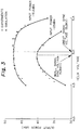
- FIG. 3 shows a relation between the helix voltage and the output voltage while FIG. 4 shows the overall configuration of the circuit periods.
- the TW tube had a helix voltage or operation voltage of 5 kV and produced a 12 GHz band 60 W output.
- the small signal synchronous voltage was determined to be 4.95 kV by both the computer simulation and the experiments.
- the great signal synchronous voltage was determined to be 5.0 V by both the computer simulation and the experiments. That is, the two voltages are substantially the same as each other.
- the velocity coefficients B of the circuit period P1 portion and P2 portion are respectively -0.0837 and 2.0063, and their difference ⁇ B is 2.0900, satisfying all the Eqs. (1)-(3). Therefore, the computer simulation and experiments proved the advantage available with the illustrative embodiment.
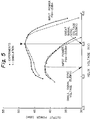
- FIG. 5 shows a relation between the helix voltage and the output power while FIG. 6 shows the overall configuration of the circuit periods.
- the small signal synchronous voltage is 5.15 kV while the great signal synchronous voltage is 5.52 V, so that a difference is as great as 370 V (6.7%).
- Such a difference brings about a corresponding decrease in gain and a corresponding variation in gain against the helix voltage. In this condition, as shown in FIG.
- the velocity coefficients B of the circuit period P1 portion and period P2 portion are respectively 0.052 and 2.005, and their difference ⁇ B is 1.953. Although such parameters satisfy the Eqs. (1)-(3), the lengths of the circuit period P0 portion and P2 portion are not adequate; the small signal synchronous voltage is far from the voltage (about 5.52 kV) that sets up the velocity coefficient B of 1.95 to 2.1 at the circuit period P2 portion.
- FIG. 7 shows a relation between the helix voltage and the output power while FIG. 8 shows the overall configuration of the circuit periods.
- the small signal synchronous voltage is 6.15 kV according to the simulation or 6.3 kV according to the experiments while the great signal synchronous voltage is 5.52 V, so that a difference is as great as 350 V to 500 V (6.7%).
- Such a difference brings about a corresponding decrease in gain and a corresponding variation in gain against the helix voltage. In this condition, as shown in FIG.
- the velocity coefficients B of the circuit period P1 portion and P2 portion are respectively -0.1459 and 2.0183 which do not satisfy the Eqs. (1)-(3). While the velocity taper portion between the circuit period P0 portion and the circuit period P1 portion is shifted to the input side, such a configuration cannot achieve the object alone, as determined by the experiments.
- a TW tube can be most effectively miniaturized if small signal synchronous and great signal synchronous signals are coincident.
- the circuit configurations shown in FIGS. 4 and 6 are based on substantially the same design parameters.
- the small signal gain is 65.5 d (for the helix voltage of 4.95 kV) while the great signal gain is about 58 dB (for the helix voltage of 5 kV), as shown in FIG. 3.
- the great signal gain is about 58 dB (for the helix voltage of 5 kV), as shown in FIG. 3.
- a uniform circuit period P0 portion and a uniform circuit period P1 portion are respectively configured short and long.
- the circuit period P0 portion and circuit period P1 portion are respectively configured long and short.
Landscapes
- Microwave Tubes (AREA)
- Microwave Amplifiers (AREA)
Applications Claiming Priority (2)
| Application Number | Priority Date | Filing Date | Title |
|---|---|---|---|
| JP7257868A JP2809155B2 (ja) | 1995-10-04 | 1995-10-04 | ヘリックス型進行波管 |
| JP257868/95 | 1995-10-04 |
Publications (2)
| Publication Number | Publication Date |
|---|---|
| EP0767480A2 true EP0767480A2 (de) | 1997-04-09 |
| EP0767480A3 EP0767480A3 (de) | 1998-12-30 |
Family
ID=17312297
Family Applications (1)
| Application Number | Title | Priority Date | Filing Date |
|---|---|---|---|
| EP96115837A Withdrawn EP0767480A3 (de) | 1995-10-04 | 1996-10-02 | Wendeltyp-Wanderfeldröhre |
Country Status (3)
| Country | Link |
|---|---|
| US (1) | US5723948A (de) |
| EP (1) | EP0767480A3 (de) |
| JP (1) | JP2809155B2 (de) |
Families Citing this family (6)
| Publication number | Priority date | Publication date | Assignee | Title |
|---|---|---|---|---|
| US6356023B1 (en) | 2000-07-07 | 2002-03-12 | Ampwave Tech, Llc | Traveling wave tube amplifier with reduced sever |
| US6356022B1 (en) | 2000-07-07 | 2002-03-12 | Ampwave Tech, Llc | Tapered traveling wave tube |
| JP6409296B2 (ja) * | 2014-03-19 | 2018-10-24 | 日本電気株式会社 | 送信機、レーダ装置及び送信電力制御方法 |
| CN105914116B (zh) * | 2016-05-10 | 2018-01-23 | 电子科技大学 | 一种超宽带微波管能量耦合结构 |
| CN106920722B (zh) * | 2016-11-24 | 2018-08-21 | 电子科技大学 | 一种基于螺距调整的空间行波管群时延的抑制方法 |
| CN106898533B (zh) * | 2016-11-24 | 2018-08-21 | 电子科技大学 | 一种基于螺旋线内径调整的空间行波管群时延的抑制方法 |
Family Cites Families (4)
| Publication number | Priority date | Publication date | Assignee | Title |
|---|---|---|---|---|
| US3324342A (en) * | 1963-07-12 | 1967-06-06 | Varian Associates | Traveling wave tube having maximum gain and power output at the same beam voltage |
| FR2463501A1 (fr) * | 1979-08-08 | 1981-02-20 | Nippon Electric Co | Tube a ondes progressives du type helicoidal |
| JPS57170440A (en) * | 1981-03-23 | 1982-10-20 | Litton Systems Inc | Travelling wave tube |
| US5162697A (en) * | 1990-08-06 | 1992-11-10 | Hughes Aircraft Company | Traveling wave tube with gain flattening slow wave structure |
-
1995
- 1995-10-04 JP JP7257868A patent/JP2809155B2/ja not_active Expired - Lifetime
-
1996
- 1996-10-02 EP EP96115837A patent/EP0767480A3/de not_active Withdrawn
- 1996-10-03 US US08/724,863 patent/US5723948A/en not_active Expired - Lifetime
Also Published As
| Publication number | Publication date |
|---|---|
| JP2809155B2 (ja) | 1998-10-08 |
| JPH09102284A (ja) | 1997-04-15 |
| US5723948A (en) | 1998-03-03 |
| EP0767480A3 (de) | 1998-12-30 |
Similar Documents
| Publication | Publication Date | Title |
|---|---|---|
| US6593695B2 (en) | Broadband, inverted slot mode, coupled cavity circuit | |
| US5469022A (en) | Extended interaction output circuit using modified disk-loaded waveguide | |
| US5723948A (en) | Helix travelling-wave tube with a maximum small signal gain at the operating voltage | |
| US4315194A (en) | Coupled cavity traveling wave tube with velocity tapering | |
| CN107452582B (zh) | 一种能够抑制谐波的宽带折叠波导行波管 | |
| US3761760A (en) | Circuit velocity step taper for suppression of backward wave oscillation in electron interaction devices | |
| US3902098A (en) | Linear beam microwave tube having means coupled to the beam upstream of input coupler and/or downstream of output coupler for varying amplitude and/or phase of r.f. component in the beam | |
| US5525864A (en) | RF source including slow wave tube with lateral outlet ports | |
| US3205398A (en) | Long-slot coupled wave propagating circuit | |
| US4149107A (en) | Backward wave oscillator tube for the production of microwave | |
| US5162697A (en) | Traveling wave tube with gain flattening slow wave structure | |
| US2824256A (en) | Backward wave tube | |
| US4378512A (en) | Helix type traveling wave tube | |
| JP3511293B2 (ja) | Tm01xモード(x>0)のクライストロン共鳴空洞 | |
| US3009078A (en) | Low noise amplifier | |
| US2911556A (en) | Backward travelling wave oscillators | |
| CA1086862A (en) | Lossless traveling wave booster tube | |
| CN116994929A (zh) | 一种行波管慢波电路设计方法、慢波电路及行波管 | |
| US4168451A (en) | Multi-cavity klystron amplifiers | |
| GB811116A (en) | Improvements in or relating to travelling wave velocity modulation devices | |
| US5059928A (en) | Mode transformer for microwave energy transmission circuit | |
| US4118671A (en) | Traveling wave tube circuit | |
| US4107572A (en) | Traveling-wave tube having phase velocity tapering means in a slow-wave circuit | |
| US3758811A (en) | Traveling wave tube linearity characteristics | |
| US6014387A (en) | Stable operating regime for traveling wave devices |
Legal Events
| Date | Code | Title | Description |
|---|---|---|---|
| PUAI | Public reference made under article 153(3) epc to a published international application that has entered the european phase |
Free format text: ORIGINAL CODE: 0009012 |
|
| AK | Designated contracting states |
Kind code of ref document: A2 Designated state(s): DE FR |
|
| PUAL | Search report despatched |
Free format text: ORIGINAL CODE: 0009013 |
|
| AK | Designated contracting states |
Kind code of ref document: A3 Designated state(s): DE FR |
|
| 17P | Request for examination filed |
Effective date: 19981124 |
|
| 17Q | First examination report despatched |
Effective date: 20010309 |
|
| RAP1 | Party data changed (applicant data changed or rights of an application transferred) |
Owner name: NEC MICROWAVE TUBE, LTD. |
|
| STAA | Information on the status of an ep patent application or granted ep patent |
Free format text: STATUS: THE APPLICATION HAS BEEN WITHDRAWN |
|
| 18W | Application withdrawn |
Effective date: 20100621 |