EP0758807A2 - Oberflächenkontaktierender elektrischer Stecker - Google Patents
Oberflächenkontaktierender elektrischer Stecker Download PDFInfo
- Publication number
- EP0758807A2 EP0758807A2 EP96305845A EP96305845A EP0758807A2 EP 0758807 A2 EP0758807 A2 EP 0758807A2 EP 96305845 A EP96305845 A EP 96305845A EP 96305845 A EP96305845 A EP 96305845A EP 0758807 A2 EP0758807 A2 EP 0758807A2
- Authority
- EP
- European Patent Office
- Prior art keywords
- buckling beam
- electrical connector
- beam element
- housing portion
- buckling
- Prior art date
- Legal status (The legal status is an assumption and is not a legal conclusion. Google has not performed a legal analysis and makes no representation as to the accuracy of the status listed.)
- Withdrawn
Links
Images


Classifications
-
- H—ELECTRICITY
- H01—ELECTRIC ELEMENTS
- H01R—ELECTRICALLY-CONDUCTIVE CONNECTIONS; STRUCTURAL ASSOCIATIONS OF A PLURALITY OF MUTUALLY-INSULATED ELECTRICAL CONNECTING ELEMENTS; COUPLING DEVICES; CURRENT COLLECTORS
- H01R13/00—Details of coupling devices of the kinds covered by groups H01R12/70 or H01R24/00 - H01R33/00
- H01R13/02—Contact members
- H01R13/193—Means for increasing contact pressure at the end of engagement of coupling part, e.g. zero insertion force or no friction
-
- G—PHYSICS
- G01—MEASURING; TESTING
- G01R—MEASURING ELECTRIC VARIABLES; MEASURING MAGNETIC VARIABLES
- G01R1/00—Details of instruments or arrangements of the types included in groups G01R5/00 - G01R13/00 and G01R31/00
- G01R1/02—General constructional details
- G01R1/06—Measuring leads; Measuring probes
- G01R1/067—Measuring probes
- G01R1/073—Multiple probes
- G01R1/07307—Multiple probes with individual probe elements, e.g. needles, cantilever beams or bump contacts, fixed in relation to each other, e.g. bed of nails fixture or probe card
- G01R1/07357—Multiple probes with individual probe elements, e.g. needles, cantilever beams or bump contacts, fixed in relation to each other, e.g. bed of nails fixture or probe card with flexible bodies, e.g. buckling beams
Definitions
- This invention generally relates to electrical connector assemblies. More particularly, the present invention relates to an improved electrical connector having buckling beam probes which are shielded to be protected from physical damage.
- Connectors for forming separable connections between electrical conductors are well known and useful. Most of these connectors employ a sliding fit between two mating, contact elements. Some connectors utilize the electrical conductors themselves, e.g. traces on a printed circuit board (PCB) or flexible wires, as one of the mating contacts. Such a design simplifies the connector assembly.
- PCB printed circuit board
- One type of contact element which has been advantageously used is described as a buckling beam test probe or contact.
- a buckling beam probe is formed with a length many times its cross-sectional area so that the probe buckles or deflects when a predetermined axial load is applied thereto.
- a long buckling beam provides a small force plus a relatively uniform force throughout its deflection or buckling range. This enables the same force to be exerted on each of a plurality of pads on a semiconductor chip regardless of the deflection of the probe produced by variations in the heights of the pads. The forces for contacting the pad must be kept small so that the pads are not damaged. Accordingly, a buckling beam contact or probe is made sufficiently long with respect to its cross-sectional area such that the force applied to the pads would be determined by the resistance to buckling of the beam.
- Buckling direction of a buckling beam contact or probe is typically controlled by accomplishing any one of the following techniques:
- a buckling beam probe or contact continues to bend without additional force.
- Such physical behavior under load is referred to as elastic instability, which typically is considered a structural failure.
- this physical behavior provides a spring contact with uniform force over a wide compliance range which is useful in high density electrical connectors.
- an active electrical connector comprises at least one electrically insulating first housing portion and at least one elongated flexible metal buckling beam element having a predetermined length and width dimension. The length dimension of the buckling beam element is greater than the width dimension.
- the at least one buckling beam element is positioned in a predetermined location on the first housing portion. Each at least one buckling beam element has a contact end and an opposed termination end.
- a preshaping or preloading member applies a predetermined load to the at least one buckling beam element in a direction substantially perpendicular to the length dimension of the buckling beam to ensure that the at least one buckling beam element will predictably bend in a predetermined direction.
- An electrically insulating second housing portion at least partially encloses the at least one first housing portion, the at least one buckling beam element, and the preloading or preshaping member.
- the second housing portion has a facing surface portion having formed therethrough at least one aperture for permitting extension of the at least one buckling beam element therethrough.
- the second housing portion is moveable, back and forth, in a direction substantially parallel to the at least one buckling beam, from a first position wherein the second housing portion protectably encloses the contact ends of the at least one buckling beam element, to a second position wherein the contact end of the at least one buckling beam element extends through the aperture.
- a mating passive electrical connector housing may be used in conjunction with the active electrical connector.
- the mating passive electrical connector housing has at least one mating electrical conductor with a surface perpendicular to and aligned with the contact end of the at least one buckling beam.
- the contact end of the at least one buckling beam electrically communicates with the at least one mating electrical conductor when mating of the active electrical connector and the passive electrical connector causes the second housing portion of the active electrical connector member to be disposed in the second position.
- an active electrical connector comprises an electrically insulating housing having a facing surface portion having formed therethrough at least one aperture.
- At least one elongated flexible metal buckling beam element has a predetermined length and width dimension. The length dimension is greater than the width dimension.
- the at least one buckling beam element is positioned in a predetermined location on the housing portion.
- Each at least one buckling beam element has a contact end and an opposed termination end.
- a retractor is operable to selectably retract the at least one buckling beam element within the electrically insulating housing.
- the retractor is moveable, back and forth, from a first position wherein the at least one buckling beam element is disposed within the housing thereby protecting the contact end of the at least one buckling beam element, to a second position wherein the contact end of the at least one buckling beam element extends through the aperture of the housing.
- a mating passive electrical connector housing also may be used in conjunction with the active electrical connector of the alternate embodiment.
- Yet another purpose of the present invention is to provide a large scale connector assembled of modular, simple components which can be readily arranged into various configurations.
- the active electrical connector 10 may be useful in providing a separable electrical connection between connectors, such as but not limited to other active or passive electrical connectors, printed circuit boards, coaxial cable assemblies, multichip modules, integrated circuits, or generally planar conductive surfaces.
- the term active electrical connector shall mean an electrical connector comprised of one or more buckling beam contacts, housings and structure therefor.
- the term passive electrical connector shall mean any electrical conductor portions, housings or structures to which the active electrical connector mates.
- one embodiment of the active electrical connector 10 comprises a housing 12 having a preloading or preshaping member 16 and at least one elongated, flexible metal conductive buckling beam element 14.
- the housing 12 comprises first and second housing portions 12a and 12b, respectively.
- the housing portions 12a and 12b are made from an electrically insulating material, such as a thermoplastic material, for example.
- thermoplastic materials include, but are not limited to polyphenylene sulfide, polyamide, acetylene-butadiene-styrene terpolymer, polytetrafluoroethylene, polyvinyl chloride, polypropylene, polyethylene, liquid crystal polymer, polyethylene imide, or other suitable engineering grade thermoplastic materials.
- the first housing portion 12a fixedly locates at least one buckling beam element 14 in a predetermined location.
- the first housing portion 12a fixedly locates a plurality of buckling beam elements in a predetermined linear array or pattern.
- the buckling beam elements may be fixedly located on the first housing portion 12a by any suitable means, such as by way of a tight fit with a shaped portion 20 of the housing 12, for example.
- a means for aligning the buckling beam elements is provided, which is illustrated as a suitably dimensioned groove or channel 22.
- the preloading or preshaping member 16 may be formed on the first housing portion 12a.
- the preloading member 16 is shown as an elongated protuberance formed integrally with the first housing portion 12a, the preloading member 16 may be any member which applies a predetermined load to each buckling beam element, in a direction substantially perpendicular to the length of each buckling beam element, such that each buckling beam element bends predictably in a predetermined direction.
- the first housing portion 12a may have formed therethrough apertures 24 for receiving threaded fasteners 26.
- the first housing portion 12a may be constructed of several separate shaped pieces of insulating material to facilitate its manufacture.
- Each buckling beam element 14 has a contact end 30 and a termination end 32.
- each termination end 32 is illustrated electrically terminated to a respective conductive trace 19 of a printed circuit board 18.
- each termination end 32 is illustrated electrically terminated to a respective coaxial cable comprising a signal wire 47 and a ground wire 48.
- each buckling beam element 14 has a length dimension which is greater than the width dimension of the buckling beam.
- the buckling beam elements 14 are formed of a suitable material which will continue to deflect over a predetermined range when a predetermined force is applied. Suitable materials include, but are not limited to, BeNi, BeCU or tungsten.
- each buckling beam element 14 causes longitudinal movement of the contact end 30 of each buckling beam element 14, as well as a small transverse movement which provides a wiping action that cleans and removes any oxide or material from the surface of the conductive element.
- That force is transmitted to the shaped portion 20 of the housing 12.
- the second housing portion 12b at least partially encloses the first housing portion 12a, the buckling beam elements 14, and the preloading means 16.
- the second housing portion has a facing surface 34 which has formed therethrough apertures 36.
- the apertures 36 are arranged in a linear pattern which mirrors the pattern of the positioned buckling beam elements 14.
- the apertures 36 are suitably dimensioned to permit extension of the buckling beam elements therethrough.
- the second housing portion 12b is moveable, back and forth along a path or travel, in a direction substantially parallel to the buckling beam elements, as indicated by the arrow 38.
- the second housing portion 12b is moveable from a first position wherein the second housing portion protectably encloses the contact ends 30 of the buckling beam elements, to a second position, wherein the contact ends of the buckling beam elements extend through the apertures 36.
- a biasing means may be employed to bias the second housing portion 12b into the first position.
- Any suitable biasing means may be employed including a spring element, or as illustrated in Figures 5, 6, and 7, predetermined buckling beam elements 40 may serve as the biasing means.
- the biasing buckling beam elements 40 may be positioned at each lateral end of the array of buckling beam elements to achieve a balanced biasing force upon the second housing portion 12b.
- These biasing buckling beam elements exert a biasing force on an interior portion of the facing surface 34 of the second housing portion. This can be easily achieved by elimination of the apertures 36 for selected buckling beams.
- the active electrical connector 10 may include a range of motion limiting member 42 to limit the back and forth travel of the second housing portion 12b.
- the active electrical connector 10 of Figures 1, 2, 3, 10 and 11 is shown electrically terminated to a plurality of coaxial cables 46.
- the active electrical connector 10 of Figures 1, 2, 3, 10 and 11 differs from the active electrical connector of Figures 5, 6, and 7 in that the termination ends 32 of the buckling beams 14 are typically shorter and contained completely within the housing 12.
- One embodiment of the active electrical connector 10 of Figures 1, 2, 3, 10 and 11 utilizes separate contacts for each signal wire 47 and for each ground wire 48.
- higher signal density in the connector can be attained by terminating more than one ground wire to one contact. This technique is known as ground commoning.
- An additional requirement for such an embodiment of the active electrical connector 10 is to provide good strain relief to transfer any load applied to a cable to the housing 12. Potting, molding, clamping, or other suitable means can be used for strain relief.
- Figure 1 is a perspective view of the active electrical connector 10 of Figure 2.
- Figure 1 illustrates the active electrical connector 10 readied for electrical connection to an electrical device 44 by use of a passive electrical connector 50.
- the passive electrical connector is a structural part which guides the active electrical connector 10 to the appropriate position as it is forced against the electrical device 44 so that the contact end 30 of each buckling beam is forced against an appropriate conductive element 49 on the electrical device 44.
- the threaded fasteners 26 are operable to screwthreadably engage threaded fixtures 28 to removably anchor the active electrical connector 10 in electrical communication with the electrical device 44. Additionally, other means than threaded fasteners 26, such as latches, clips, or detents may be employed to secure the active electrical connector 10 to the electrical device 44, or the passive electrical connector 50.
- FIGS 3, 10 and 11 illustrate an alternate embodiment of the active electrical connector 10 of the present invention.
- This embodiment includes an electrically insulating housing 12 having a facing surface 34, which has formed therethrough at least one aperture 36. At least one buckling beam element is provided which has been described in detail hereinabove.
- the active electrical connector 10 of Figures 3, 10 and 11 is shown electrically connected to a plurality of coaxial cables 46, it should be understood the active electrical connector 10 may be terminated to any suitable electrical conductor, such as but not limited to other electrical connectors, a printed circuit board, a multichip module, an integrated circuit, or any other suitable electrically conductive planar array.
- the housing 12 of the active electrical connector of Figures 3, 10 and 11 is not moveable to expose the contact ends 30 of the buckling beam elements 14.
- the active electrical connector of Figures 3, 10, and 11 comprises a means for selectably retracting the buckling beam elements 14 within the electrically insulating housing.
- FIG 3 illustrates one embodiment of an active electrical connector having a means for selectably retracting the buckling beam elements 14 within the electrically insulating housing 12.
- the selectable buckling beam retracting means may comprise a sliding cam type assembly which is illustrated at 70.
- each sliding cam assembly 70 includes a series of identically shaped cam ramps 51 which are slidable back and forth within the housing from a first position ( Figure 18), wherein the cam ramps engage respective buckling beam elements such that the buckling beam elements are retracted within the housing 12, to a second position ( Figure 19), wherein the cam ramps disengage the respective buckling beam elements such that the buckling beam elements extend through the housing 12.
- the sliding cam assembly 70 may function in conjunction with suitable features (not shown) of a passive electrical connector 50 to move in a predetermined direction during mating and unmating of the active electrical connector 10 with the passive electrical connector 50.
- suitable features not shown
- the cam assembly 70 slides to the second position (cam ramps disengaged).
- the cam assembly 70 slides to the first position (cam ramps engaged).
- buckling beam retracting means include, but are not limited to, a rotary cam assembly 80, such as that illustrated in Figures 10-17, for example.
- the rotary cam assembly 80 is suitable for selectably retracting the buckling beam elements 14 within the housing 12.
- the rotary cam system comprises a shaft 82 supported within the housing 12, cams 84, and at least one pair of opposed levers 86. As best illustrated by Figures 10 and 11, the opposed levers 86 are offset 90°, as will be explained in further detail hereinafter.
- first levers 88 are pushed by a beam 89 extending from the passive electrical connector.
- the cam shaft 82 rotates the cams 84 to permit the buckling beam elements 14 to extend through the apertures 36, from the housing 12, toward electrical conductors 49 of the passive electrical connector 50.
- second levers 90 rotate the cam shaft 82 back to its original position by action of a beam 92. Beam 92 does not engage the second levers 90 during mating.
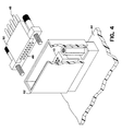
- Figure 4 illustrates an electrical connection which is comprised of an active electrical connector 10, a passive electrical connector 50, and an electrical shield housing 62.
- the shield housing 62 may be comprised of either a conductive or insulative structural material.
- a conductive material such as a metal
- both structural protection and electrical shielding can be achieved.
- an insulative material such as an insulative material of the type for housing 12, structural protection is afforded along with protection against unwanted electrical connections during handling of respective components.
- the active electrical connector 10 illustrated in Figure 5 is prepared for through hole mounting to a printed circuit board. This preparation primarily consists of positioning the termination ends 32 of the buckling beam elements 14 substantially parallel to the buckling beam elements with suitable adjustment to the spacing so that they will align and protrude through an array of apertures in the printed circuit board to which the connector will be mounted. These apertures are often plated through holes suitable for connection to the termination ends 32 by soldering.
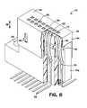
- the active electrical connector 10 illustrated in Figure 6 is prepared for vertical surface mounting to a printed circuit board. This preparation primarily consists of positioning the termination ends 32 of the buckling beams 14 at outward pointing right angles to the buckling beam elements.
- FIG 8 is a perspective view of an embodiment of a passive electrical connector 50 of the present invention as applied to coaxial cables.
- each coaxial cable signal wire 47 is formed to provide a flat, circular conductive contact element 49.
- These conductive contact elements are accurately positioned within a housing assembly 52 to form a predetermined array on a face 53.
- the housing assembly 52 is formed of a structural insulating material, such as the type of materials described for the housing 12, for example.
- Figure 9 is a perspective view of an alternate embodiment of the passive electrical connector 50 of Figure 8.
- the wires are formed into flat, square contacts.
Landscapes
- Coupling Device And Connection With Printed Circuit (AREA)
- Connector Housings Or Holding Contact Members (AREA)
- Details Of Connecting Devices For Male And Female Coupling (AREA)
Applications Claiming Priority (2)
| Application Number | Priority Date | Filing Date | Title |
|---|---|---|---|
| US514335 | 1995-08-11 | ||
| US08/514,335 US5597317A (en) | 1995-08-11 | 1995-08-11 | Surface mating electrical connector |
Publications (2)
| Publication Number | Publication Date |
|---|---|
| EP0758807A2 true EP0758807A2 (de) | 1997-02-19 |
| EP0758807A3 EP0758807A3 (de) | 1998-11-18 |
Family
ID=24046740
Family Applications (1)
| Application Number | Title | Priority Date | Filing Date |
|---|---|---|---|
| EP96305845A Withdrawn EP0758807A3 (de) | 1995-08-11 | 1996-08-09 | Oberflächenkontaktierender elektrischer Stecker |
Country Status (3)
| Country | Link |
|---|---|
| US (1) | US5597317A (de) |
| EP (1) | EP0758807A3 (de) |
| JP (1) | JPH09237661A (de) |
Families Citing this family (9)
| Publication number | Priority date | Publication date | Assignee | Title |
|---|---|---|---|---|
| JP2717376B2 (ja) * | 1995-03-09 | 1998-02-18 | 日本航空電子工業株式会社 | Zifコネクタ |
| US5885095A (en) * | 1996-05-28 | 1999-03-23 | Teradyne, Inc. | Electrical connector assembly with mounting hardware and protective cover |
| US6024579A (en) * | 1998-05-29 | 2000-02-15 | The Whitaker Corporation | Electrical connector having buckling beam contacts |
| US6524123B2 (en) * | 2001-01-19 | 2003-02-25 | Agilent Technologies, Inc. | Self-aligning, quick-release connector |
| US7598727B1 (en) * | 2006-09-12 | 2009-10-06 | Xilinx, Inc. | Probe card head protection device for wafer sort set up |
| US8635798B2 (en) | 2011-08-23 | 2014-01-28 | Tyco Electronics Corporation | Communication connector system for a weapon |
| US8721355B2 (en) * | 2012-02-01 | 2014-05-13 | Tyco Electronics Corporation | Electrical connector with hood |
| JP5947640B2 (ja) * | 2012-07-03 | 2016-07-06 | 矢崎総業株式会社 | 端子金具と基板の接続構造 |
| US10644458B2 (en) * | 2017-03-31 | 2020-05-05 | Intel Corporation | Shielded interconnect array |
Family Cites Families (30)
| Publication number | Priority date | Publication date | Assignee | Title |
|---|---|---|---|---|
| US3193793A (en) * | 1963-03-14 | 1965-07-06 | Kenneth W Plunkett | Electronic connector |
| US3441898A (en) * | 1967-04-06 | 1969-04-29 | Nils Ingvar Nodfelt | Connection device for electric cables |
| US3731258A (en) * | 1971-09-22 | 1973-05-01 | Int Standard Electric Corp | Underwater connection |
| US3911361A (en) * | 1974-06-28 | 1975-10-07 | Ibm | Coaxial array space transformer |
| US3806801A (en) * | 1972-12-26 | 1974-04-23 | Ibm | Probe contactor having buckling beam probes |
| US4038599A (en) * | 1974-12-30 | 1977-07-26 | International Business Machines Corporation | High density wafer contacting and test system |
| US3963986A (en) * | 1975-02-10 | 1976-06-15 | International Business Machines Corporation | Programmable interface contactor structure |
| US4027935A (en) * | 1976-06-21 | 1977-06-07 | International Business Machines Corporation | Contact for an electrical contactor assembly |
| US4066312A (en) * | 1976-06-28 | 1978-01-03 | International Business Machines Corporation | High density cable connector |
| US4227149A (en) * | 1978-05-30 | 1980-10-07 | International Business Machines Corporation | Sensing probe for determining location of conductive features |
| US4554506A (en) * | 1981-06-30 | 1985-11-19 | International Business Machines Corporation | Modular test probe |
| US4506215A (en) * | 1981-06-30 | 1985-03-19 | International Business Machines Corporation | Modular test probe |
| US4518910A (en) * | 1983-06-30 | 1985-05-21 | International Business Machines Corporation | Buckling beam twist probe contactor assembly with spring biased stripper plate |
| US4622514A (en) * | 1984-06-15 | 1986-11-11 | Ibm | Multiple mode buckling beam probe assembly |
| DE3473651D1 (en) * | 1984-06-22 | 1988-09-29 | Ibm Deutschland | Buckling beam test probe assembly |
| US4734046A (en) * | 1984-09-21 | 1988-03-29 | International Business Machines Corporation | Coaxial converter with resilient terminal |
| US4816754A (en) * | 1986-04-29 | 1989-03-28 | International Business Machines Corporation | Contactor and probe assembly for electrical test apparatus |
| DE3773904D1 (de) * | 1987-03-27 | 1991-11-21 | Ibm Deutschland | Kontaktsonden-anordnung zur elektrischen verbindung einer pruefeinrichtung mit den kreisfoermigen anschlussflaechen eines prueflings. |
| US4963822A (en) * | 1988-06-01 | 1990-10-16 | Manfred Prokopp | Method of testing circuit boards and the like |
| US5137461A (en) * | 1988-06-21 | 1992-08-11 | International Business Machines Corporation | Separable electrical connection technology |
| US4901013A (en) * | 1988-08-19 | 1990-02-13 | American Telephone And Telegraph Company, At&T Bell Laboratories | Apparatus having a buckling beam probe assembly |
| DE3903060A1 (de) * | 1989-02-02 | 1990-08-09 | Minnesota Mining & Mfg | Vorrichtung zum pruefen von integrierten schaltungsanordnungen |
| US4966556A (en) * | 1989-06-13 | 1990-10-30 | General Datacomm, Inc. | Electrical connector for direct connection to plated through holes in circuit board |
| US5256073A (en) * | 1989-06-13 | 1993-10-26 | General Datacomm, Inc. | Electrical connectors for direct connection to plated through holes in circuit board |
| US5015946A (en) * | 1990-02-26 | 1991-05-14 | Tektronix, Inc. | High density probe |
| US5061192A (en) * | 1990-12-17 | 1991-10-29 | International Business Machines Corporation | High density connector |
| US5225777A (en) * | 1992-02-04 | 1993-07-06 | International Business Machines Corporation | High density probe |
| US5248262A (en) * | 1992-06-19 | 1993-09-28 | International Business Machines Corporation | High density connector |
| US5259781A (en) * | 1992-11-18 | 1993-11-09 | International Business Machines Corporation | Electrical connector alignment and actuation assembly |
| US5281150A (en) * | 1993-01-05 | 1994-01-25 | International Business Machines Corporation | Method and apparatus for connecting cable to the surface of printed circuit boards or the like |
-
1995
- 1995-08-11 US US08/514,335 patent/US5597317A/en not_active Expired - Lifetime
-
1996
- 1996-08-08 JP JP20973196A patent/JPH09237661A/ja active Pending
- 1996-08-09 EP EP96305845A patent/EP0758807A3/de not_active Withdrawn
Also Published As
| Publication number | Publication date |
|---|---|
| US5597317A (en) | 1997-01-28 |
| JPH09237661A (ja) | 1997-09-09 |
| EP0758807A3 (de) | 1998-11-18 |
Similar Documents
| Publication | Publication Date | Title |
|---|---|---|
| EP0498530B1 (de) | System zur Durchschaltung von elektrischen Kontakten | |
| US5634801A (en) | Electrical interconnect contact system | |
| US5358411A (en) | Duplex plated epsilon compliant beam contact and interposer | |
| US5308252A (en) | Interposer connector and contact element therefore | |
| US3915537A (en) | Universal electrical connector | |
| US6592407B2 (en) | High-speed card edge connector | |
| US6039590A (en) | Electrical connector with relatively movable two-part housing | |
| US20070287336A1 (en) | Electrical connectors with alignment guides | |
| EP0514134A2 (de) | Modularer elektrischer Verbinder | |
| EP0540260B1 (de) | Elektrischer Verbinder zur Verbindung einer Leiterplatte mit einem Kabel | |
| US8007308B2 (en) | Electrical connector assembly | |
| US5388996A (en) | Electrical interconnect contact system | |
| US5002494A (en) | Printed circuit board edge connector | |
| US5174764A (en) | Connector assembly having surface mounted terminals | |
| KR100344048B1 (ko) | Pga 패키지용의 점검 가능한 전기 커넥터 | |
| US20050064737A1 (en) | Method for interconnecting multiple printed circuit boards | |
| US12424785B2 (en) | Receptacle connector | |
| EP0003435B1 (de) | Elektrischer Steckverbinder für die Herstellung von Verbindungen zwischen einem flachen flexiblen Kabel und einem weiteren Steckverbinder | |
| JP3325050B2 (ja) | コネクタ組立体 | |
| US5597317A (en) | Surface mating electrical connector | |
| WO2009105380A2 (en) | Electrical termination device | |
| US5597320A (en) | Zero insertion force electrical connector and terminal | |
| KR19990007851A (ko) | 전기 커넥터 및 커넥터 어셈블리 | |
| US6923655B2 (en) | Electrical connector for interconnecting two intersected printed circuit boards | |
| US5697794A (en) | High density connector assembly |
Legal Events
| Date | Code | Title | Description |
|---|---|---|---|
| PUAI | Public reference made under article 153(3) epc to a published international application that has entered the european phase |
Free format text: ORIGINAL CODE: 0009012 |
|
| AK | Designated contracting states |
Kind code of ref document: A2 Designated state(s): DE ES FR GB IT SE |
|
| PUAL | Search report despatched |
Free format text: ORIGINAL CODE: 0009013 |
|
| AK | Designated contracting states |
Kind code of ref document: A3 Designated state(s): DE ES FR GB IT SE |
|
| 17P | Request for examination filed |
Effective date: 19990506 |
|
| 17Q | First examination report despatched |
Effective date: 19990830 |
|
| STAA | Information on the status of an ep patent application or granted ep patent |
Free format text: STATUS: THE APPLICATION IS DEEMED TO BE WITHDRAWN |
|
| 18D | Application deemed to be withdrawn |
Effective date: 20010301 |