EP0758772B1 - Mehrprozessoranordnung und Verfahren zur Synchronisierung zwischen Prozessoren - Google Patents
Mehrprozessoranordnung und Verfahren zur Synchronisierung zwischen Prozessoren Download PDFInfo
- Publication number
- EP0758772B1 EP0758772B1 EP96250170A EP96250170A EP0758772B1 EP 0758772 B1 EP0758772 B1 EP 0758772B1 EP 96250170 A EP96250170 A EP 96250170A EP 96250170 A EP96250170 A EP 96250170A EP 0758772 B1 EP0758772 B1 EP 0758772B1
- Authority
- EP
- European Patent Office
- Prior art keywords
- state
- cache
- memory
- processor system
- processing units
- Prior art date
- Legal status (The legal status is an assumption and is not a legal conclusion. Google has not performed a legal analysis and makes no representation as to the accuracy of the status listed.)
- Expired - Lifetime
Links
Images


Classifications
-
- G—PHYSICS
- G06—COMPUTING OR CALCULATING; COUNTING
- G06F—ELECTRIC DIGITAL DATA PROCESSING
- G06F12/00—Accessing, addressing or allocating within memory systems or architectures
- G06F12/02—Addressing or allocation; Relocation
- G06F12/08—Addressing or allocation; Relocation in hierarchically structured memory systems, e.g. virtual memory systems
- G06F12/0802—Addressing of a memory level in which the access to the desired data or data block requires associative addressing means, e.g. caches
- G06F12/0806—Multiuser, multiprocessor or multiprocessing cache systems
- G06F12/0815—Cache consistency protocols
Definitions
- the present invention relates to a multi-processor system and a method for synchronizing among a plurality of processors, and more particularly to a multi-processor system and a method for synchronizing among a plurality of processors with a simplified cache protocol.
- a cache memory state of the entry having the variable "X” is referred to as a "shared” state.
- the state of the corresponding entry of the processing unit #2 becomes an "invalid” state
- the state of this entry of the processing unit #1 becomes an "update” state.
- variable "X" When the variable "X" is subsequently read by the processing unit #2, after the entry of the cache memory of the processing unit #1 is again written into the shared memory, this entry is transferred to the cache memory of the processing unit #2, and the state of the entries of both processing units #1 and #2 becomes the "shared" state.
- variable "Y" is included in the same entry as the above-described variable "X"
- the entry of the processing unit #2 is invalidated. Accordingly, the data of the variable "X" would also be deleted from the cache memory.
- an object of the present invention is to simplify a cache protocol in a multi-processor system to realize a high-speed operation.
- a multi-processor system having a plurality of processing units, at least one of the processing units comprises a cache memory for storing entries, each being a copy of an entry in at least one memory module; and a state memory which stores a cache state table for storing a synchronization state of the cache memory with regard to the copies in other cache memories of the processing units of the multi-processor system, and a cache state for each entry in the cache memory wherein the cache memory is available for access if the synchronization state indicates a most recent state, and wherein the cache state indicates one of a plurality of states, the plurality of states including an invalid state for indicating that any data has ever been loaded from the at least one memory module, but that none of the data remains valid; a valid state for indicating that a data is valid said multi-processor characterized in that the plurality of states further includes a reset state for indicating that no data has ever been loaded from the at least one memory module to the cache memory, wherein said cache memory is available for access
- a cache memory is controlled with a simplified cache protocol, and intermediate cache states are omitted.
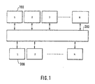
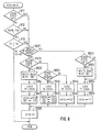
- a multi-processor system according to an embodiment of the present invention comprises N (where N is an integer) processing units 100, M (where M is an integer and M can be less than, equal to, or greater than N according to the designer's requirements) memory modules 300, and a network 200 coupling together the processing units 100 and memory modules 300.
- the network 200 allows each processing unit 100 to communicate with any of the memory modules 300.
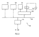
- the processing unit 100 in the multi-processor system of the present invention comprises a processor 110, a cache memory 120, a cache state table 130, a synchronization counter 140, a state updater 150, a local bus 160, and a network interface 170.
- the processor 110 and the cache memory 120 are connected via the local bus 160.
- the processing unit 100 is connected to the network 200 via the network interface 170.
- the cache state table 130 holds a cache state of each of the entries in a cache memory 120.
- the synchronization counter 140 counts every time a synchronization instruction (command) is executed.
- the cache state table 130 is updated by the state updater 150 connected to the local bus 160.
- the cache memory 120 includes a data memory (not shown) and an address tag memory (not shown) for managing addresses of data stored in the cache memory 120.
- a synchronization instruction is executed every time an entry in the cache memory 120 is modified by other processing units.
- the synchronization counter 140 (abbreviated as "SC” in the drawings) is incremented every time the synchronization instruction is executed in the processor 110.
- the sync instruction is executed when an entry in the cache memory 120 is modified as discussed below.
- the sync counter 140 provides a value representing the present synchronization level of the processing unit 100.
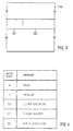
- the cache state table 130 stores a cache state 131 and a cache synchronization count 132 (abbreviated as "CC" in the drawings) in correspondence with the respective entries of the cache memory 120.
- the cache state 131 indicates the state of a corresponding entry of the cache memory 130.
- the cache state 131 has various states such as an "invalid” state and a "shared” state, as described below.
- the cache synchronization count 132 shows the synchronization level of the data of the respective entry. Thus, the value of the synchronization counter 140 when the respective entry is loaded in the cache memory 120 is stored into the cache synchronization count 132.
- the cache memory 120 according to a first embodiment of the present invention has five kinds of states for representing the cache state.
- the "R (Reset)” state indicates an initial state, and implies that since no data is loaded from the memory modules 300 after the system is initiated, the content of the data cannot be assured.
- the "I (Invalid)” state denotes an invalid state, and represents such an invalidated (e.g., updated) state after the valid data has been loaded once.
- the "CE (Clean Exclusive)” state denotes that only a specific cache memory 120 has a copy of the memory module 300, and also that the copy coincides with the content of the memory module 300.
- the "CS (Clean Shared)” state represents that other cache memories 120 also have copies of the memory modules 300, and also that these copies coincide with the content of the memory module 300.
- the "DE (Dirty Exclusive)” state indicates that only a specific cache memory 120 has a copy of the memory module 300, and also that this copy does not coincide with the content of the memory module 300.
- each state of all entries has an "R” state.
- each state of the respective entries becomes either the "CE” state or the "CS" state.
- the data is invalid and thus cannot be read in the conventional cache protocol.
- the data is forcibly read in a predetermined case even under the "I" state.
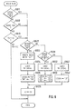
- cache state 131 of the cache memory 120 (e.g., of the local processor) is checked to determine whether the cache state 131 is under the "CS" state (step S511). If the cache state 131 of the cache memory is under the "CS" state, then other cache memories of the multi-processor system are invalidated (step S512). Each cache state 131 of the other cache memories becomes the "I" state after step S512.
- the data is written into the cache memory 120 (step S513).
- the cache synchronization count 132 of a corresponding entry in the cache state table 130 is set to have the value of the synchronization counter 140 (step S514).
- the cache state 131 becomes the "DE" state (step S515).
- cache state 131 of the cache memory 120 (e.g., of the local processor) is checked to determine whether the cache state 131 is under "R" state (step S611).
- step S611 if cache state 131 is under "R” state, then operations beginning at step S622 are executed, because the correct (e.g., most recent) data has not yet been entered. Conversely, if cache state 131 is not under "R” state, then an address tag in the tag memory (not illustrated) is checked to determine whether an address to be accessed matches the address tag (step S612), because there is a probability that the correct (latest) data is entered.
- step S612 if the address tag does not match, then operations beginning at step S622 are executed, because the required data is not left in the cache memory. If the address tag matches, then the cache synchronization count 132 and the value of the synchronization counter 140 are compared (step S613), because there may be an invalidated data in the cache memory.
- step S613 if the cache synchronization count 132 (CC) is smaller than the value (SC) of the synchronization counter 140, then the operations beginning at step S622 are executed, because the data in the cache memory is non-synchronized data. If the cache synchronization count 132 is equal to the value of the synchronization counter 140, then the data is directly read without conventional cache protocol operations, because the data in the cache memory is synchronized data.
- Such a read operation with a simplified cache protocol is one of the features of the first embodiment.
- step S622 The operations beginning at step S622 are similar to those of the conventional copy-back cache protocol. That is, when any of the cache states in the cache memories of other processing units is in the "DE" state, after the entry with the "DE” state is written back to the memory module 300 (step S623), this entry is loaded from the memory module 300 into the cache memory 120 of its own (e.g., the local) processing unit (step S624).
- the cache state 131 With respect to the entry loaded on its own processing unit (e.g., the local processing unit) and the entry with the "DE” state among other processing units, the cache state 131 becomes the "CS" state (step S625), and the cache synchronization count 132 (CC) becomes the value (SC) of the synchronization counter 140 (step S626).
- a write operation on a cache miss-hit (e.g., a "miss")
- the operations are performed by the read operation on a cache miss-hit and the write operation on a cache-hit.
- variable "Y" belongs to the same entry as the variable "X”.
- the cache state of the processing unit #2 becomes the "I” state (step S512 of FIG. 5)
- the cache state of the processing unit #1 becomes the "DE” state (step S515 of FIG. 5).
- the cache synchronization count 132 (CC) is equal to the value (SC) of the synchronization counter 140, synchronization is assured (step S613 of FIG. 6). Consequently, the variable "X" can be read from the entry whose cache state is under the "I” state. Furthermore, when the processing unit refers to the variable "Y”, the variable can also be read from the entry under the "DE” state.
- the "R" state indicative of the initial state is newly provided as the cache state. Furthermore, the synchronization counter 140 is employed which is incremented every time the synchronization instruction is executed.
- the cache synchronization count 132 stores the value of the synchronization counter 140. If (1) the cache state is not under the "R" state, (2) the tags match, and (3) the cache synchronization count 132 is equal to the value of the synchronization counter 140, then the cache memory can be accessed with the simplified cache protocol.
- step S621 an operation similar to that of the first embodiment is executed except for the following. That is, in such an entry which is updated immediately after a read operation on a cache miss-hit (step S621), the corresponding data is loaded from the memory module (step S654), and then the cache state (e.g., of the local cache) becomes the "I" state (step S655).
- the cache state e.g., of the local cache
- step S655 e.g., a write operation on both a cache-hit and a cache miss-hit, and a read operation on a cache-hit are similar to those of the first embodiment.
- the judgement as to "whether or not the entry is updated immediately after" may be clearly defined in the program, or may be analyzed by a compiler.
- the cache state of the processing unit #2 is set to the "I" state (step S655 of FIG. 8). This is because the operation may be processed at high-speed by omitting the intermediate state required by the conventional system as shown in FIG. 12.
- this entry in addition to the first embodiment, as to an entry which may be previously updated by other processing units after the next synchronization instruction is executed, this entry becomes the "I" state during the loading of the data.
- the intermediate cache state required by the conventional system may be omitted, and therefore the operation can be further executed at high-speed.
- the network 200 is assumed to function such that a change of cache state can be instructed from a respective processing unit to all of the remaining processing units at the same time.
- a common bus and the like may correspond to this sort of network.
- a block copy table 310 as illustrated in FIG. 10 may be provided with respect to each of the memory modules 300.
- the block copy table 310 is coupled to each processing unit 100, and stores therein a copy state 311 indicating which cache memory of the processing unit has a copy of the memory module 300 corresponding to each of the entries in the cache memory 120.
- the copy state #1 when the copy state #1 is equal to "1", this implies that there is a copy in the cache memory within the processing unit #1.
- the copy state #2 is equal to "0", it implies that there is no copy in the cache memory within the processing unit #2.
- the processing unit having the copy of the memory module can be specified with reference to the block copy table 310, and the cache protocol operations can be individually controlled.
- the initial state "R" is newly provided as the cache state and the synchronization counter which is incremented every time the synchronization instruction is executed, it is possible to access the cache memory with a simplified cache protocol.
- this entry As to an entry which is previously recognized to be updated by the other processing units after the next synchronization instruction is executed, this entry is set under an invalid state when the entry is loaded. Consequently, the intermediate cache state may be omitted and a high-speed operation with greater reliability may be achieved.
Landscapes
- Engineering & Computer Science (AREA)
- Theoretical Computer Science (AREA)
- Physics & Mathematics (AREA)
- General Engineering & Computer Science (AREA)
- General Physics & Mathematics (AREA)
- Memory System Of A Hierarchy Structure (AREA)
- Multi Processors (AREA)
Claims (13)
- Ein Mehrprozessorsystem mit einer Mehrzahl Prozeß- oder Verarbeitungseinheiten, mindestens einem Speichermodul und einem Netzwerk, das die Verarbeitungseinheiten und mindestens ein Speichermodul verbindet, wobei mindestens eine der Verarbeitungseinheiten umfaßt:einen Cache-Speicher zum Speichern von Eingaben, von denen jede eine Kopie einer Eingabe in mindestens einem Speichermodul ist, undeinen Zustandsspeicher, der eine Cache-Zustandstabelle zum Speichern eines Synchronisationszustands des Cache-Speichers in Bezug auf die Kopien in anderen Cache-Speichern der Verarbeitungseinheiten des Mehrprozessorsystems und einen Cache-Zustand für jede Eingabe in dem Cache-Speicher speichert,wobei der Cache-Speicher für einen Zugriff verfügbar ist, wenn der Synchronisationszustand den neuesten Zustand angibt,und wobei der Cache-Zustand einen einer Mehrzahl Zustände angibt, wobei die Mehrzahl Zustände umfaßt:einen ungültigen Zustand zum Angeben, daß irgendwelche Daten überhaupt von dem mindestens einen Speichermodul ausgeladen worden sind, jedoch keines der Daten gültig bleibt,einen gültigen Zustand zum Angeben, daß Daten gültig sind,wobei besagtes Mehrprozessorsystem dadurch gekennzeichnet ist, daß die Mehrzahl Zustände außerdem einen zurückgesetzten Zustand zum Angeben umfaßt, daß keinerlei Daten überhaupt je von dem mindestens einen Speichermodul her in den Cache-Speicher geladen worden sind, wobei der Cache-Speicher zum Zugriff verfügbar ist, wenn zusätzlich der Cache-Zustand einen anderen Zustand als den zurückgesetzten Zustand angibt.
- Das Mehrprozessorsystem nach Anspruch 1, bei dem die mindestens eine der Verarbeitungseinheiten außerdem umfaßt:
einen Synchronisationszähler zum Synchronisationszählen unter den Verarbeitungseinheiten. - Das Mehrprozessorsystem nach Anspruch 2, bei dem der Synchronisationszähler einen Wert zum Einstellen des Synchronisationszustands in der Cache-Zustandstabelle bereitstellt, wenn entsprechende Daten von dem mindestens einen Speichermodul her geladen worden sind.
- Das Mehrprozessorsystem nach Anspruch 3, bei dem der Cache-Speicher für einen Zugriff verfügbar ist, wenn der Synchronisationszustand mit dem Wert des Synchronisationszählers übereinstimmt.
- Das Mehrprozessorsystem nach Anspruch 1, bei dem der gültige Zustand umfaßt:einen reinen, exklusiven Zustand zum Angeben, daß nur der Cache-Speicher einer jeweiligen der mindestens einen Verarbeitungseinheit in dem Mehrprozessorsystem eine Kopie des mindestens einen Speichermoduls aufweist und daß die Kopie mit dem Inhalt des mindestens einen Speichermoduls übereinstimmt,einen reinen, geteilten Zustand zum Angeben, daß andere Cache-Speicher der Prozessoren des Mehrprozessorsystems Kopien des mindestens einen Speichers aufweisen und die Kopien mit dem Inhalt des mindestens einen Speichermoduls übereinstimmen, undeinen unreinen, exklusiven Zustand zum Angeben, daß nur der Cache-Speicher der jeweiligen mindestens einen der Verarbeitungseinheiten in dem Mehrprozessorsystem eine Kopie des mindestens einen Speichermoduls aufweist und daß die Kopie nicht mit dem Inhalt des mindestens einen Speichermoduls übereinstimmt.
- Das Mehrprozessorsystem nach Anspruch 2, bei dem der Cache-Speicher für einen Zugriff verfügbar ist, wenn der Synchronisationszustand mit dem Wert des Synchronisationszählers übereinstimmt und der Cache-Zustand einen anderen Zustand als den zurückgesetzten Zustand angibt.
- Das Mehrprozessorsystem nach Anspruch 1, das weiterhin Mittel umfaßt, um im voraus zu beurteilen, ob der Cache-Zustand durch einen nachfolgenden Betriebsvorgang derselben mindestens einen der Verarbeitungseinheiten ungültig gemacht wird.
- Das Mehrprozessorsystem nach Anspruch 2, das weiterhin Mittel umfaßt, um im voraus zu beurteilen, ob ein Cache-Zustand einer der mindestens einen der Verarbeitungseinheiten durch einen nachfolgenden Betriebsvorgang einer anderen Verarbeitungseinheit ungültig gemacht wird.
- Das Mehrprozessorsystem nach Anspruch 1, wobei das Netzwerk einen gemeinsamen Bus aufweist.
- Das Mehrprozessorsystem nach Anspruch 1, bei dem mindestens eine der Verarbeitungseinheiten außerdem umfaßt:
eine Block-Kopietabelle, die mit der mindestens einen der Verarbeitungseinheiten verbunden und in Bezug auf jedes Speichermodul des mindestens einen Speichermoduls vorgesehen ist, zum Speichern eines Kopierzustands, der angibt, welcher Cache-Speicher anderer jeweiliger Verarbeitungseinheiten eine Kopie des mindestens einen Speichermoduls aufweist, die jeder der Eingaben in dem Cache-Speicher entspricht. - Das Mehrprozessorsystem nach Anspruch 1, bei dem jede Eingabe in dem Cache-Speicher eine Mehrzahl Wörter enthält.
- Das Mehrprozessorsystem nach Anspruch 2, bei dem ein Cache-Synchronisationszählwert gültig ist, selbst wenn der Cache-Zustand den ungültigen Zustand hat.
- Das Mehrprozessorsystem nach Anspruch 1, bei dem eine Eingabe eine Mehrzahl Variable umfaßt.
Applications Claiming Priority (3)
| Application Number | Priority Date | Filing Date | Title |
|---|---|---|---|
| JP204148/95 | 1995-08-10 | ||
| JP20414895 | 1995-08-10 | ||
| JP7204148A JPH0950400A (ja) | 1995-08-10 | 1995-08-10 | マルチプロセッサシステム |
Publications (3)
| Publication Number | Publication Date |
|---|---|
| EP0758772A2 EP0758772A2 (de) | 1997-02-19 |
| EP0758772A3 EP0758772A3 (de) | 1998-02-11 |
| EP0758772B1 true EP0758772B1 (de) | 2001-11-14 |
Family
ID=16485637
Family Applications (1)
| Application Number | Title | Priority Date | Filing Date |
|---|---|---|---|
| EP96250170A Expired - Lifetime EP0758772B1 (de) | 1995-08-10 | 1996-08-09 | Mehrprozessoranordnung und Verfahren zur Synchronisierung zwischen Prozessoren |
Country Status (5)
| Country | Link |
|---|---|
| US (1) | US5923855A (de) |
| EP (1) | EP0758772B1 (de) |
| JP (1) | JPH0950400A (de) |
| CA (1) | CA2182841C (de) |
| DE (1) | DE69616903T2 (de) |
Families Citing this family (19)
| Publication number | Priority date | Publication date | Assignee | Title |
|---|---|---|---|---|
| JPH09204403A (ja) * | 1996-01-26 | 1997-08-05 | Hitachi Ltd | 並列計算機 |
| US6314495B1 (en) * | 1998-01-07 | 2001-11-06 | International Business Machines Corporation | Method and apparatus for executing multiply-initiated, multiply-sourced variable delay system bus operations |
| US6272593B1 (en) | 1998-04-10 | 2001-08-07 | Microsoft Corporation | Dynamic network cache directories |
| US8028318B2 (en) | 1999-07-21 | 2011-09-27 | Touchtunes Music Corporation | Remote control unit for activating and deactivating means for payment and for displaying payment status |
| US6526480B1 (en) | 1998-12-10 | 2003-02-25 | Fujitsu Limited | Cache apparatus and control method allowing speculative processing of data |
| US6286082B1 (en) * | 1999-04-19 | 2001-09-04 | Sun Mocrosystems, Inc. | Apparatus and method to prevent overwriting of modified cache entries prior to write back |
| US6553409B1 (en) * | 1999-07-09 | 2003-04-22 | Microsoft Corporation | Background cache synchronization |
| US7181539B1 (en) * | 1999-09-01 | 2007-02-20 | Microsoft Corporation | System and method for data synchronization |
| CN1264091C (zh) * | 1999-11-22 | 2006-07-12 | 阿茨达科姆公司 | 分布式高速缓存同步协议 |
| KR100394827B1 (ko) * | 1999-12-22 | 2003-08-21 | 엘지전자 주식회사 | 이동통신교환기의 프로세서 재시동을 위한 프로그램 및데이터 적재방법 |
| US6615281B1 (en) * | 2000-05-05 | 2003-09-02 | International Business Machines Corporation | Multi-node synchronization using global timing source and interrupts following anticipatory wait state |
| US6651145B1 (en) * | 2000-09-29 | 2003-11-18 | Intel Corporation | Method and apparatus for scalable disambiguated coherence in shared storage hierarchies |
| JP4085389B2 (ja) * | 2003-12-24 | 2008-05-14 | 日本電気株式会社 | マルチプロセッサシステム、マルチプロセッサシステムにおける一貫性制御装置及び一貫性制御方法 |
| TW200717246A (en) * | 2005-06-24 | 2007-05-01 | Koninkl Philips Electronics Nv | Self-synchronizing data streaming between address-based producer and consumer circuits |
| US7555607B2 (en) * | 2005-11-10 | 2009-06-30 | Hewlett-Packard Development Company, L.P. | Program thread syncronization for instruction cachelines |
| US7587555B2 (en) * | 2005-11-10 | 2009-09-08 | Hewlett-Packard Development Company, L.P. | Program thread synchronization |
| US20090319804A1 (en) * | 2007-07-05 | 2009-12-24 | Broadcom Corporation | Scalable and Extensible Architecture for Asymmetrical Cryptographic Acceleration |
| US8943058B1 (en) * | 2009-12-14 | 2015-01-27 | Teradata Us, Inc. | Calculating aggregates of multiple combinations of a given set of columns |
| US8438335B2 (en) * | 2010-09-28 | 2013-05-07 | Intel Corporation | Probe speculative address file |
Family Cites Families (2)
| Publication number | Priority date | Publication date | Assignee | Title |
|---|---|---|---|---|
| US5018063A (en) * | 1988-12-05 | 1991-05-21 | International Business Machines Corporation | Method for reducing cross-interrogate delays in a multiprocessor system |
| US5680576A (en) * | 1995-05-05 | 1997-10-21 | Silicon Graphics, Inc. | Directory-based coherence protocol allowing efficient dropping of clean-exclusive data |
-
1995
- 1995-08-10 JP JP7204148A patent/JPH0950400A/ja active Pending
-
1996
- 1996-08-05 US US08/692,346 patent/US5923855A/en not_active Expired - Fee Related
- 1996-08-07 CA CA002182841A patent/CA2182841C/en not_active Expired - Fee Related
- 1996-08-09 DE DE69616903T patent/DE69616903T2/de not_active Expired - Fee Related
- 1996-08-09 EP EP96250170A patent/EP0758772B1/de not_active Expired - Lifetime
Also Published As
| Publication number | Publication date |
|---|---|
| JPH0950400A (ja) | 1997-02-18 |
| EP0758772A2 (de) | 1997-02-19 |
| DE69616903T2 (de) | 2002-07-18 |
| US5923855A (en) | 1999-07-13 |
| CA2182841C (en) | 2000-05-16 |
| CA2182841A1 (en) | 1997-02-11 |
| EP0758772A3 (de) | 1998-02-11 |
| DE69616903D1 (de) | 2001-12-20 |
Similar Documents
| Publication | Publication Date | Title |
|---|---|---|
| EP0758772B1 (de) | Mehrprozessoranordnung und Verfahren zur Synchronisierung zwischen Prozessoren | |
| US5740400A (en) | Reducing cache snooping overhead in a multilevel cache system with multiple bus masters and a shared level two cache by using an inclusion field | |
| EP0833248B1 (de) | Rechnersystem mit Speicherung der Speicheraktualisierungsgeschichte | |
| US5274787A (en) | Method of copy-back cache coherence control and tightly coupled multi-processor system with split transfer system bus | |
| EP0828217B1 (de) | Cachespeicherräumungsvorrichtung und hiermit versehenes Rechnersystem | |
| US4959777A (en) | Write-shared cache circuit for multiprocessor system | |
| US6839810B2 (en) | Consistency control device merging updated memory blocks | |
| JP2566701B2 (ja) | 共有キャッシュ内のデータ・ユニットに対する所有権の変更制御装置 | |
| US6272602B1 (en) | Multiprocessing system employing pending tags to maintain cache coherence | |
| US5146603A (en) | Copy-back cache system having a plurality of context tags and setting all the context tags to a predetermined value for flushing operation thereof | |
| US6625698B2 (en) | Method and apparatus for controlling memory storage locks based on cache line ownership | |
| JP2002163148A (ja) | キャッシュメモリー付マルチ処理システム | |
| US6341339B1 (en) | Apparatus and method for maintaining data coherence within a cluster of symmetric multiprocessors | |
| JP2002197073A (ja) | キャッシュ一致制御装置 | |
| JP2746530B2 (ja) | 共有メモリマルチプロセッサ | |
| WO1997004392A1 (en) | Shared cache memory device | |
| JP2000512050A (ja) | マイクロプロセッサキャッシュの一貫性 | |
| US6061766A (en) | Non-inclusive cache method using pipelined snoop bus | |
| EP0153109B1 (de) | Cache-Kohärenz-Anordnung | |
| CN119292963B (zh) | 一种多处理器的数据访问控制架构及控制方法 | |
| JPH08263374A (ja) | キャッシュ制御方法およびそれを用いたマルチプロセッサシステム | |
| JPH06208507A (ja) | キャッシュメモリシステム | |
| JP2593222B2 (ja) | マルチプロセッサシステムのインタロック方式 | |
| JPH0127455B2 (de) | ||
| JPH10149307A (ja) | チェックポイント処理方法及び記録媒体 |
Legal Events
| Date | Code | Title | Description |
|---|---|---|---|
| PUAI | Public reference made under article 153(3) epc to a published international application that has entered the european phase |
Free format text: ORIGINAL CODE: 0009012 |
|
| AK | Designated contracting states |
Kind code of ref document: A2 Designated state(s): DE FR GB NL |
|
| PUAL | Search report despatched |
Free format text: ORIGINAL CODE: 0009013 |
|
| AK | Designated contracting states |
Kind code of ref document: A3 Designated state(s): DE FR GB NL |
|
| 17P | Request for examination filed |
Effective date: 19980219 |
|
| 17Q | First examination report despatched |
Effective date: 19990324 |
|
| GRAG | Despatch of communication of intention to grant |
Free format text: ORIGINAL CODE: EPIDOS AGRA |
|
| GRAG | Despatch of communication of intention to grant |
Free format text: ORIGINAL CODE: EPIDOS AGRA |
|
| GRAG | Despatch of communication of intention to grant |
Free format text: ORIGINAL CODE: EPIDOS AGRA |
|
| GRAH | Despatch of communication of intention to grant a patent |
Free format text: ORIGINAL CODE: EPIDOS IGRA |
|
| GRAH | Despatch of communication of intention to grant a patent |
Free format text: ORIGINAL CODE: EPIDOS IGRA |
|
| GRAA | (expected) grant |
Free format text: ORIGINAL CODE: 0009210 |
|
| AK | Designated contracting states |
Kind code of ref document: B1 Designated state(s): DE FR GB NL |
|
| REF | Corresponds to: |
Ref document number: 69616903 Country of ref document: DE Date of ref document: 20011220 |
|
| REG | Reference to a national code |
Ref country code: GB Ref legal event code: IF02 |
|
| ET | Fr: translation filed | ||
| PLBE | No opposition filed within time limit |
Free format text: ORIGINAL CODE: 0009261 |
|
| STAA | Information on the status of an ep patent application or granted ep patent |
Free format text: STATUS: NO OPPOSITION FILED WITHIN TIME LIMIT |
|
| 26N | No opposition filed | ||
| PGFP | Annual fee paid to national office [announced via postgrant information from national office to epo] |
Ref country code: GB Payment date: 20050803 Year of fee payment: 10 |
|
| PGFP | Annual fee paid to national office [announced via postgrant information from national office to epo] |
Ref country code: DE Payment date: 20050804 Year of fee payment: 10 |
|
| PGFP | Annual fee paid to national office [announced via postgrant information from national office to epo] |
Ref country code: FR Payment date: 20050809 Year of fee payment: 10 |
|
| PGFP | Annual fee paid to national office [announced via postgrant information from national office to epo] |
Ref country code: NL Payment date: 20050815 Year of fee payment: 10 |
|
| PG25 | Lapsed in a contracting state [announced via postgrant information from national office to epo] |
Ref country code: NL Free format text: LAPSE BECAUSE OF NON-PAYMENT OF DUE FEES Effective date: 20070301 Ref country code: DE Free format text: LAPSE BECAUSE OF NON-PAYMENT OF DUE FEES Effective date: 20070301 |
|
| GBPC | Gb: european patent ceased through non-payment of renewal fee |
Effective date: 20060809 |
|
| NLV4 | Nl: lapsed or anulled due to non-payment of the annual fee |
Effective date: 20070301 |
|
| REG | Reference to a national code |
Ref country code: FR Ref legal event code: ST Effective date: 20070430 |
|
| PG25 | Lapsed in a contracting state [announced via postgrant information from national office to epo] |
Ref country code: GB Free format text: LAPSE BECAUSE OF NON-PAYMENT OF DUE FEES Effective date: 20060809 |
|
| PG25 | Lapsed in a contracting state [announced via postgrant information from national office to epo] |
Ref country code: FR Free format text: LAPSE BECAUSE OF NON-PAYMENT OF DUE FEES Effective date: 20060831 |