EP0750268B1 - Réseau de diffusion pseudo-axonique permettant de créer des champs récepteurs variables - Google Patents
Réseau de diffusion pseudo-axonique permettant de créer des champs récepteurs variables Download PDFInfo
- Publication number
- EP0750268B1 EP0750268B1 EP96401358A EP96401358A EP0750268B1 EP 0750268 B1 EP0750268 B1 EP 0750268B1 EP 96401358 A EP96401358 A EP 96401358A EP 96401358 A EP96401358 A EP 96401358A EP 0750268 B1 EP0750268 B1 EP 0750268B1
- Authority
- EP
- European Patent Office
- Prior art keywords
- cell
- network
- cells
- output
- comparator
- Prior art date
- Legal status (The legal status is an assumption and is not a legal conclusion. Google has not performed a legal analysis and makes no representation as to the accuracy of the status listed.)
- Expired - Lifetime
Links
Images



Classifications
-
- G—PHYSICS
- G06—COMPUTING OR CALCULATING; COUNTING
- G06N—COMPUTING ARRANGEMENTS BASED ON SPECIFIC COMPUTATIONAL MODELS
- G06N3/00—Computing arrangements based on biological models
- G06N3/02—Neural networks
- G06N3/06—Physical realisation, i.e. hardware implementation of neural networks, neurons or parts of neurons
- G06N3/063—Physical realisation, i.e. hardware implementation of neural networks, neurons or parts of neurons using electronic means
- G06N3/065—Analogue means
Definitions
- the present invention relates to networks electronic mail to create fields receivers or projectors, according to a principle that tries to mimic what is going on in the nervous system of sentient beings living. This is why sometimes the specialists of this domain call these networks "pseudo-axonic trees".
- Such networks are used to create systems in which each cell of an axon tree allows to communicate with a large number of selected cells from another group (or "layer"), the number of cells in this other layer of cells being determined by the very topology of this axon tree.
- a field of application of such networks using of axon pseudo-neuronal trees, is that of the character recognition.
- the network examined in this document includes layers composed of cells which in each layer are laterally connected to each other by through so-called "RG" connecting elements (for resistance-conductance) preferably having a nonlinear conduction characteristic, and which are typically transistors.
- RG resistance-conductance
- Each cell has a connection node in which can be injected with a current which can propagate laterally in the layer towards neighboring cells at through the corresponding RG elements.
- Cells as well achieved by this command pulse form in the layer a circular shape configuration called "bubble" by specialists.
- each cell in an emitting layer can be connected by its own axon tree to cells of a receiving layer and propagate information materialized from the currents injected into the cells through the conduction elements.
- the extent of a bubble in the layer depends on first place of the intensity of the injected current.
- the object of the invention is to provide a network of distribution of the "pseudo-axon neuronic tree" type which, based on the principles set out in the abovementioned document by P. Heim, presents a simple structure and effective, while presenting better performances, in particular that allowing to generate bubbles of non-uniform dimensions.
- the invention therefore relates to a pseudo-axonic network information dissemination including a plurality of cells connected together for the transmission of information by connecting elements, preferably with a conduction characteristic not linear, each cell comprising a connection node whose potential is representative of the excited state of said cell and to which at least one of said is connected connecting elements, said connection node of each cell also being inserted in a serial circuit comprising a current source and an element current consumer to fix said potential, said network being characterized in that each cell comprises also a switching element between said source of current and said connection node, each element switch can be closed selectively by activation pulses, as well as a comparator for compare said potential of the connection node to a threshold voltage, the output of said comparator forming the leaving said cell and delivering information of representative output of the excitation rate of this cell resulting from activations of one or more any cells in said network.
- the information elementary to be processed by the cell can be a command or activation pulse which by closing the switching element, causes the temporary injection of a current in the connection node of the cell, to communicate the information represented by said activation pulse to cell nodes preselected neighbors of the network, in the form of temporary currents flowing through the connecting elements between these cells and taken from the injected current.
- the information to be disseminated not only a quantitative aspect by the intensity of the injected current, but also a temporal aspect, last being represented either by the duration of the pulse even more advantageously by the frequency of control pulses applied to a cell considered.
- the information provided by a given cell can be formed by a accumulation of basic information provided respectively on each appearance somewhere in the network of a command pulse capable of causing the excitation of the cell under consideration.
- the document EP 0 517 097 describes a network having cells whose connection nodes can receive different potentials under the action of a signal collective selection which acts on the whole of a row of cells.
- This selection signal allows activate amplifiers in each cell operational authorizing the application of potentials to another operational amplifier whose output is connected to the cell connection node.
- no switch element is provided to allow selective injection on the plane spatial of a current in the connection node of every cell let alone such an injection which either time-selective.
- comparator 7n The inverting input of comparator 7n is connected to a source 9 delivering a threshold voltage Vth.
- the elements RG 8n, 8rn and 8sn can be simple ohmic resistors but as shown they are preferably formed by MOS transistors allowing to generate non-circular bubbles in the network.
- the voltages Vr1, Vr2 and Vr3 applied respectively on the grids of the MOS transistors 8n, 8rn and 8sn can be different from each other. So, we can choose the direction of propagation of the currents according to the three possible directions defined by the network.
- the comparator 7n delivers a signal on the output 10n of the cell according to the result of the comparison between the threshold voltage Vth and the potential of node 1n.
- this output can be connected to one or more other cells of the network constituting with the cell Cn a pseudo-axonic tree, for example.
- a usage circuit (not shown), such as a charge accumulation device, a counter pulse or a frequency / voltage converter or current delivering a useful signal which is representative of the temporal behavior of the cell in question.
- configurations two-dimensional can form groups of cells that we can imagine constituting layers, connected to neighboring layers via connections between the outputs and the nodes of the cells.
- layer should not be understood as if the cells were actually arranged in physically superimposed layers, only the electrical connections between the nodes of the cells and the outputs of these can translate this notion.
- a complex network with several layers can therefore physically be planar and be realized in the form of a single or multiple integrated circuit chips, per example.
- the cell node 1n Cn is connected to the source of current 3n through switch 2n, the latter being ordered via an lln command line at which can be applied an activation signal In of the cell in the form of a current pulse or several successive current pulses depending on the information that we want to distribute in the network. This point will be explained in more detail later in the description.
- Figure 2 represents a concrete example of a cell according to the invention.
- the cell includes a first connected serial circuit between power source 4 and ground 6.
- this series circuit are inserted three transistors M1, M2 and M3.
- the transistor M1 forms the current source 3n. His tension grid is applied to it by a command line 12.
- the transistor M2 determines the potential of the node 1n, a Vu voltage being applied for this purpose to its grid at through a command line 13.
- the transistor M3 constitutes the switch 2n, its grid being connected to the 11n command line.
- the cell also includes a second series circuit in which the transistors M4 and M5 are inserted together constituting the comparator 7n.
- the 10n outlet of the cell is taken from the node between these two transistors.
- the threshold voltage Vth is applied to the gate of transistor M4 via a line 14.
- the gate of transistor M5 is connected to node 1n.
- the elements 8n, 8rn and 8sn are formed by respective transistors M6a, M6b and M6c whose circuits source-drain are inserted between the 1n node of the cell considered and the equivalent transistors of three cells neighbors.
- the gates of these transistors M6a, M6b and M6c are connected to respective control lines 15a, 15b and 15c on which are applied the voltages of command Vr1, Vr2 and Vr3 whose role will appear by the after.
- Figure 3 shows in more detail part of a hexagonal diffusion network, each cell of this network being surrounded by a symbolic circle which delimits it by compared to other cells. So the figure represents Cn, Cn-1, Cn + 1, Rn, Sn, Tn and Un cells. These cells are connected to each other by RG elements, such as 8n, 8n-1, 8rn and 8sn for example belonging respectively to two contiguous cells. In this configuration, the cells are therefore rigorously identical. It will be noted that the control voltages applied to these RG elements are the same according to diagonals of the network.
- the transistors which connect the cells Cn-1, Cn and Cn + 1, Tn and Rn cells and Un and Sn cells respectively, are controlled by the same voltage Vr1, while the transistors which connect cells Un, Cn and Sn, Cn-1 and Un cells and Rn and Cn + 1 cells are controlled by the voltage Vr2 respectively, etc.
- Figure 4 shows the diagram of Figure 3 in multiplying to illustrate the construction of a part of a two-dimensional hexagonal network of very large dimensions, only cell Cn being detailed separately in the circle designated by 19. This part includes 45 cells. In practice, such a network may include several thousand cells.
- the hexagonal layout has an important technological advantage in that it allows a density of maximum cells without the need to provide crossings of cell interconnections.
- Figure 5 shows a broadcast network one-dimensional according to the invention and produced using cells such as that shown in Figures 1 and 2 except that they are simplified by not comprising only one RG element leading to the neighboring cell and well heard therefore that only one command line for application the control voltage.
- This figure 5 shows nine cells referenced Cn-5 to Cn + 3, cell Cn being assumed to receive a pulse In command line on its 11n command line.
- the ratio of the currents Iinj and Iu (see figure 1) circulating on both sides of node 1n first determines the number of cells that will be activated on each side of the receiving Cn cell the activation pulse In. In other words, this ratio determines the number of cells in which the current injected into node 1n could generate a potential sufficient to trigger the comparator of a cell. In the case shown, it has been assumed that this ratio is equal to seven, since, as can be seen in the figure 5, cells Cn-4 to Cn + 2 produce an impulse at their exit. We therefore consider here that the "bubble" on which disseminates the information represented by the applied pulse on cell Cn, has a range of seven cells. As this range depends on the current ratio Iinj / Iu, we can notice that it is determined in reality and first place by the ratio of the applied voltages respectively on lines 12 and 14 (see Figure 2).
- Figure 6 shows a one-dimensional network composed of simplified cells according to the invention, this network also being provided with means for determining the direction of the propagation of information in the network.
- this network can, as desired, be made unidirectional in each direction in terms of propagation some information.
- the control grid of this switch element is connected to the line .... 11n-1, 11n, 11n + 1 .... of the corresponding cell by through an inverter .... 17n-1, 17n, 17n + 1 .
- this network has 100 cells, if the cell comparators 7n switch for a voltage of node 1n corresponding to a current Iu of 2 nA and if the current injected into the node of the cell receiving the command pulse is 100 nA, the "bubble" will span fifty cells in the network.
- Figure 6 highlights another characteristic advantageous according to the invention which consists of possibility of not showing a signal at the output that of the last cell that must be activated for the dissemination of information.
- each cell is equipped with a door NAND .... 18n-1, 18n, 18n + 1 with one of the inputs connected to the output 10n-1, 10n, 10n + 1 .... of the corresponding cell and at the other entrance to the NAND gate from the previous cell.
- a signal does not appear at the output of a cell only if it is itself activated, at the same time as the previous cell. This amounts to a single signal appears at the exit of the network (in this case at the exit of cell Cn + 3).
- FIG 7A shows a concrete example a simplified cell used in the network according to the Figure 6, the diagram of the NAND gate 18n not being there represented.
- This cell has only one transistor M6 forming element RS, since it is intended to be part of a one-dimensional network.
- the switching transistor 16n and the inverter 17n in Figure 6 are made using transistors respective M7, M8 and M9.
- FIG. 7B shows a similar diagram for a cell intended for a two-dimensional network with possibility of blocking the dissemination of information in a given broadcast direction.
- Figure 8 symbolically represents an example of a combination of one-dimensional networks unidirectional on the one hand and bidirectional networks on the other hand, which have just been described above. he is a broadcasting system with two networks R1x and R2x for direction X and two networks R1y, R2y for direction Y, respectively, these networks being constructed according to the diagram in Figure 6. In addition, the system has two two-dimensional networks CR1 and CR2 according to Figures 3 and 4.
- This system can include a very large number of cells, for example several thousand to fix the ideas.
- the assembly represented thus constitutes a system of diffusion making it possible to generate receptive fields in function of cell activation in each network two-dimensional, one of which can be exciting and the other inhibitor.
- the four one-dimensional networks R1x, R2x, R1y and R2y are capable of generating a shift between the position of a target cell Cn and the center of the part excitatory or inhibitory of the receptive field.
- the system of Figure 8 is capable to generate receptive fields comparable to those of cells of the visual cortex including cells simple, complex and hypercomplex cells and contour cells.
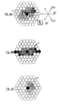
- FIGS. 9A to 9E illustrate the operation of a two-dimensional diffusion network of the type described above Figures 3 and 4 and implementing the features of the invention.
- each cell is represented by a circle. Furthermore, in FIG. 9A, there are indicated by voltage vectors Vr1, Vr2 and Vr3, the directions in which act these voltages in the network by activating the communication transistors with the cells neighbors.
- a CC injection cell of the network is activated by a current pulse.
- this cell may (or may not) be different for each activation pulse depending on the place where this pulse is applied to the network.
- the ratio Iinj / Ii applied to the CC injection cell is for example equal to 21, a value which is here chosen only as an example.
- the voltages Vr1 and Vr2 are chosen to equal values, while the voltage Vr3 is equal to zero.
- the current pulse spreads through the network to from the injection cell and activates all surrounding cells for which the control voltages have authorized communication with neighboring cells respective and for which at the same time the current corresponding to the part (s) of the impulse activation (nen) t, is (are) sufficient (s) to trigger their comparator 7n.
- the shape of the "bubble" the configuration of all activated cells in this two-dimensional network
- the cell CC1 is activated by the voltage Vr1 by taking its share of the current pulse that comes directly to it from the CC injection cell.
- Cell D4 for example is activated by current shares which reach it neighboring cells due to the presence of Vrl voltages and Vr2 at the same time.
- each 10n output of a cell can be connected to an operating circuit already mentioned above, such as a device for accumulating charges of the capacitor type for example, shown schematically in 20 in Figure 9A for one of the D5 cells of the network.
- the quantity of charges stored in these devices of charge accumulation can thus correspond to the number successive excitations of these cells by train successive activation pulses applied to cells network injection.
- the data provided by each of cells will therefore have a "weight" all the more important as the number of times the current pulses reaching activate it will be larger.
- the invention makes it possible to create a true network of pseudo-axonic trees capable of process pieces of information by combining them according to rules dictated by the application of the parameters of order cells. More specifically, thanks to connection transistors between cells (such as transistors 8n, 8rn and 8sn of figure 1), we can conveniently determine the scattering distance between cells and thus form information "bubbles" of very diverse forms.
- the invention allows to program the receiver field parameters in a distribution network by the simple determination of current reports in each cell of it.
- the proposed circuit for each cell in its simplest version contains only ten transistors so that, thanks to the invention, a single usual size integrated circuit chip can house a network comprising a very large number of cells.
Landscapes
- Engineering & Computer Science (AREA)
- Physics & Mathematics (AREA)
- Health & Medical Sciences (AREA)
- Life Sciences & Earth Sciences (AREA)
- Biomedical Technology (AREA)
- Biophysics (AREA)
- Theoretical Computer Science (AREA)
- Evolutionary Computation (AREA)
- General Engineering & Computer Science (AREA)
- Data Mining & Analysis (AREA)
- Artificial Intelligence (AREA)
- General Health & Medical Sciences (AREA)
- Molecular Biology (AREA)
- Computing Systems (AREA)
- Computational Linguistics (AREA)
- General Physics & Mathematics (AREA)
- Mathematical Physics (AREA)
- Software Systems (AREA)
- Neurology (AREA)
- Data Exchanges In Wide-Area Networks (AREA)
- Image Analysis (AREA)
- Design And Manufacture Of Integrated Circuits (AREA)
Description
- la figure 1 est un schéma fonctionnel d'une cellule pour un réseau bidimensionnel de diffusion pseudo-axonique, conçu selon l'invention;
- la figure 2 est le schéma d'un exemple de réalisation concret d'une cellule de réseau selon la figure 1;
- la figure 3 est un schéma de quelques cellules d'un réseau bidimensionnel selon l'invention, composé de cellules telles que celles représentées sur les figures 1 et 2;
- la figure 4 représente très symboliquement une partie d'un réseau, du type hexagonal de grandes dimensions, construit selon l'invention, à partir du schéma de base représentée sur la figure 3;
- la figure 5 représente le schéma d'un réseau unidimensionnel utilisant des cellules simplifiées selon l'invention;
- la figure 6 représente le schéma d'un réseau unidimensionnel et unidirectionnel utilisant également des cellules simplifiées selon l'invention;
- la figure 7A montre le schéma d'un exemple de réalisation concret d'une cellule utilisée dans le réseau de la figure 6;
- la figure 7B montre le schéma concret d'un exemple de cellule pour un réseau hexagonal du type des figures 2 et 3 et comportant des moyens pour permettre le blocage de la diffusion dans une direction de diffusion donnée;
- la figure 8 représente symboliquement le schéma très simplifié d'un système de diffusion réalisé à l'aide de réseaux de cellules conçus selon l'invention; et
- les figures 9A à 9E montrent, à titre d'exemple, plusieurs illustrations du fonctionnement d'une partie d'un réseau bidimensionnel suivant l'invention.
- un interrupteur 2n relié par ailleurs à travers une source de courant 3n à une ligne 4 raccordée à une source d'alimentation (non représentée);
- un transistor 5n relié à la masse 6 qui est l'autre pôle de la source d'alimentation, ce transistor étant un élément consommateur qui assure la polarisation du noeud 1n;
- l'entrée non-inverseuse d'un comparateur 7n; et
- les bornes respectives de trois éléments de liaison 8n, 8rn et 8sn, de type RG, (résistance/conductance) appartenant respectivement à la cellule n considérée et destinés à être connectés à des cellules voisines du réseau. Par exemple, l'élément RG 8n est connecté au noeud 1n-1 de la cellule Cn-1.
Claims (10)
- Réseau pseudo-axonique de diffusion d'information comprenant une pluralité de cellules (Cn) connectées entre elles pour la transmission de l'information par des éléments de liaison (8n, 8rn, 8sn), de préférence à caractéristique de conduction non linéaire, chaque cellule comportant un noeud de connexion (1n) dont le potentiel est représentatif de l'état excité de ladite cellule et auquel est relié au moins un desdits éléments de liaison (8n, 8rn, 8sn), ledit noeud de connexion (1n) de chaque cellule étant également inséré dans un circuit série comportant une source de courant (3n) et un élément consommateur de courant (5n) pour fixer ledit potentiel, ledit réseau étant caractérisé en ce que chaque cellule (Cn) comporte également un élément interrupteur (2n) entre ladite source de courant (3n) et ledit noeud de connexion (1n), chaque élément interrupteur pouvant être fermé sélectivement par des impulsions d'activation, ainsi qu'un comparateur (7n) pour comparer ledit potentiel du noeud de connexion à une tension de seuil (Vth), la sortie dudit comparateur formant la sortie de ladite cellule et délivrant une information de sortie représentative du taux d'excitation de cette cellule résultant d'activations d'une ou de plusieurs cellules quelconques dudit réseau.
- Réseau suivant la revendication 1 réalisé avec des transistors CMOS, caractérisé en ce que ledit élément interrupteur (2n) est un transistor (M3) dont la grille est reliée à une ligne de commande (lln) pour la réception desdites impulsions d'activation.
- Réseau suivant les revendications 1 et 2, caractérisé en ce que chaque cellule comporte également des moyens de blocage (16n, 17n) montés en série avec ledit élément de liaison (8n, 8rn, 8sn) et connectés à ladite ligne de commande (11n) de telle manière qu'ils bloquent la connexion avec une cellule voisine (Cn-1) simultanément à la fermeture dudit élément interrupteur (2n).
- Réseau suivant la revendication 3, caractérisé en ce que lesdits moyens de blocage sont formés par un transistor (CMOS) inséré en série avec ledit élément de liaison (8n, 8rn, 8sn) et dont la grille est connectée à ladite ligne de commande (11n).
- Réseau suivant l'une quelconque des revendications 1 à 4, caractérisé en ce que chaque cellule comporte également une porte logique (18n) raccordée par l'une de ses entrées à la sortie dudit comparateur (7n) et par une autre entrée à la sortie d'une cellule voisine (Cn+1) et dont la sortie constitue la sortie de ladite cellule (Cn).
- Réseau suivant la revendication 5, caractérisé en ce que la sortie dudit comparateur (7n) est connectée à un circuit d'exploitation (20) destiné à délivrer un signal utile réprésentatif du comportement temporel de la cellule considérée.
- Réseau suivant la revendication 6, caractérisé en ce que ledit circuit d'exploitation est un dispositif d'accumulation de charges, un compteur ou analogue.
- Réseau suivant l'une quelconque des revendications 1 à 7, caractérisé en ce qu'il est de type hexagonal, chaque cellule comportant six éléments de liaison (8n, 8rn, 8sn).
- Réseau suivant la revendication 8, caractérisé en ce que lesdits éléments de liaison (8n, 8rn, 8sn) sont commandés par des tensions de commande (Vr1, Vr2, Vr3) communes selon des diagonales dudit réseau.
- Réseau suivant l'une quelconque des revendications 4 à 6, caractérisé en ce qu'il comporte des rangées de cellules (R1x, R2x, R1y, R2y) disposées par paires selon des axes perpendiculaires, les rangées correspondant à un même axe comportant des moyens de blocage agissant respectivement dans des sens opposés.
Applications Claiming Priority (2)
| Application Number | Priority Date | Filing Date | Title |
|---|---|---|---|
| FR9507578 | 1995-06-23 | ||
| FR9507578A FR2735890B1 (fr) | 1995-06-23 | 1995-06-23 | Cellule pour reseau electronique de diffusion permettant de creer des champs recepteurs dans des reseaux pseudo-axonique et reseau en comportant application |
Publications (2)
| Publication Number | Publication Date |
|---|---|
| EP0750268A1 EP0750268A1 (fr) | 1996-12-27 |
| EP0750268B1 true EP0750268B1 (fr) | 2000-01-19 |
Family
ID=9480338
Family Applications (1)
| Application Number | Title | Priority Date | Filing Date |
|---|---|---|---|
| EP96401358A Expired - Lifetime EP0750268B1 (fr) | 1995-06-23 | 1996-06-20 | Réseau de diffusion pseudo-axonique permettant de créer des champs récepteurs variables |
Country Status (4)
| Country | Link |
|---|---|
| US (1) | US5771337A (fr) |
| EP (1) | EP0750268B1 (fr) |
| DE (1) | DE69606231T2 (fr) |
| FR (1) | FR2735890B1 (fr) |
Families Citing this family (2)
| Publication number | Priority date | Publication date | Assignee | Title |
|---|---|---|---|---|
| US7426500B2 (en) * | 2002-10-29 | 2008-09-16 | Neven Dragojlovic | Parallel computer architecture of a cellular type, modifiable and expandable |
| US7596589B2 (en) * | 2004-04-12 | 2009-09-29 | University Of Florida Research Foundation, Inc. | Time-mode analog computation circuits and methods |
Family Cites Families (4)
| Publication number | Priority date | Publication date | Assignee | Title |
|---|---|---|---|---|
| JP2824780B2 (ja) * | 1989-04-18 | 1998-11-18 | 科学技術振興事業団 | 論理回路 |
| US5361328A (en) * | 1989-09-28 | 1994-11-01 | Ezel, Inc. | Data processing system using a neural network |
| US5218440A (en) * | 1991-06-07 | 1993-06-08 | Rockwell International Corporation | Switched resistive neural network for sensor fusion |
| US5530953A (en) * | 1991-11-15 | 1996-06-25 | Yasuo Nagazumi | Apparatus for relocating spatial information for use in data exchange in a parallel processing environment |
-
1995
- 1995-06-23 FR FR9507578A patent/FR2735890B1/fr not_active Expired - Fee Related
-
1996
- 1996-06-20 US US08/667,822 patent/US5771337A/en not_active Expired - Fee Related
- 1996-06-20 EP EP96401358A patent/EP0750268B1/fr not_active Expired - Lifetime
- 1996-06-20 DE DE69606231T patent/DE69606231T2/de not_active Expired - Fee Related
Also Published As
| Publication number | Publication date |
|---|---|
| DE69606231D1 (de) | 2000-02-24 |
| EP0750268A1 (fr) | 1996-12-27 |
| FR2735890A1 (fr) | 1996-12-27 |
| US5771337A (en) | 1998-06-23 |
| FR2735890B1 (fr) | 1997-08-29 |
| DE69606231T2 (de) | 2000-09-07 |
Similar Documents
| Publication | Publication Date | Title |
|---|---|---|
| EP3663988B1 (fr) | Neurone artificiel pour puce neuromorphique à synapses résistives | |
| US11062204B2 (en) | Voltage controlled highly linear resistive elements | |
| FR2667169A1 (fr) | Circuit de production de haute tension pour un circuit de memoire a semiconducteur. | |
| FR3050050A1 (fr) | Neurone artificiel | |
| WO2019219618A1 (fr) | Synapse artificielle commutee | |
| WO2014135801A1 (fr) | Organe à neurone artificiel et memristor | |
| FR3106681A1 (fr) | Architecture neuromorphique | |
| FR3089037A1 (fr) | Circuit neuronal apte à mettre en œuvre un apprentissage synaptique | |
| WO2022171632A1 (fr) | Circuit neuromorphique et procédé d'entraînement associé | |
| EP3138050A2 (fr) | Neurone artificiel mono-composant à base d'isolants de mott, réseau de neurones artificiels et procédé de fabrication correspondants | |
| WO1980001632A1 (fr) | Systeme de traitement de signaux a attenuateur electronique multivoies et a reglages memorises | |
| Shastri et al. | Photonic spike processing: ultrafast laser neurons and an integrated photonic network | |
| EP0750268A1 (fr) | Cellule pour réseau électronique de diffusion permettant de créer des champs récepteurs dans des réseaux pseudo-axoniques et réseau en comportant application | |
| FR2850768A1 (fr) | Dispositif electronique configurable a granularite mixte | |
| EP1925079B1 (fr) | Commutateur de courant a paire differentielle de transistors alimente par une faible tension vcc | |
| FR2532777A1 (fr) | Circuit de translation de signaux | |
| FR2750817A1 (fr) | Generateur d'impulsions electroniques programmables en duree et en frequence | |
| EP3549070A1 (fr) | Dispositif et procède de modulation, synapse artificielle comportant ledit dispositif de modulation, procède de plasticité a court terme dans un réseau de neurones artificiels comportant ladite synapse artificielle | |
| EP0772359B1 (fr) | Dispositif de filtrage pour traiter une pluralité de canaux dans un système de distribution de télévision par câble | |
| EP0938732B1 (fr) | Cellule electronique analogique, notamment destinee a etre implantee dans un circuit integre, et circuit integre comportant de telles cellules | |
| EP0849659B1 (fr) | Dispositif numérique d'initialisation d'un circuit intégré | |
| EP0917288B1 (fr) | Cellule comportant une pseudo-capacité notamment pour rétine artificielle | |
| EP0617359B1 (fr) | ContrÔleur à logique floue | |
| EP0720173A1 (fr) | Element de memoire statique du type bascule latch | |
| FR2671207A1 (fr) | Reseau neuronal a operateurs binaires et procedes pour sa realisation. |
Legal Events
| Date | Code | Title | Description |
|---|---|---|---|
| PUAI | Public reference made under article 153(3) epc to a published international application that has entered the european phase |
Free format text: ORIGINAL CODE: 0009012 |
|
| AK | Designated contracting states |
Kind code of ref document: A1 Designated state(s): CH DE FR GB LI |
|
| 17P | Request for examination filed |
Effective date: 19970520 |
|
| 17Q | First examination report despatched |
Effective date: 19980707 |
|
| GRAG | Despatch of communication of intention to grant |
Free format text: ORIGINAL CODE: EPIDOS AGRA |
|
| GRAG | Despatch of communication of intention to grant |
Free format text: ORIGINAL CODE: EPIDOS AGRA |
|
| GRAH | Despatch of communication of intention to grant a patent |
Free format text: ORIGINAL CODE: EPIDOS IGRA |
|
| GRAH | Despatch of communication of intention to grant a patent |
Free format text: ORIGINAL CODE: EPIDOS IGRA |
|
| GRAA | (expected) grant |
Free format text: ORIGINAL CODE: 0009210 |
|
| AK | Designated contracting states |
Kind code of ref document: B1 Designated state(s): CH DE FR GB LI |
|
| REG | Reference to a national code |
Ref country code: CH Ref legal event code: EP |
|
| REF | Corresponds to: |
Ref document number: 69606231 Country of ref document: DE Date of ref document: 20000224 |
|
| GBT | Gb: translation of ep patent filed (gb section 77(6)(a)/1977) |
Effective date: 20000314 |
|
| PLBE | No opposition filed within time limit |
Free format text: ORIGINAL CODE: 0009261 |
|
| STAA | Information on the status of an ep patent application or granted ep patent |
Free format text: STATUS: NO OPPOSITION FILED WITHIN TIME LIMIT |
|
| 26N | No opposition filed | ||
| REG | Reference to a national code |
Ref country code: GB Ref legal event code: IF02 |
|
| PGFP | Annual fee paid to national office [announced via postgrant information from national office to epo] |
Ref country code: GB Payment date: 20040615 Year of fee payment: 9 |
|
| PGFP | Annual fee paid to national office [announced via postgrant information from national office to epo] |
Ref country code: FR Payment date: 20040628 Year of fee payment: 9 |
|
| PGFP | Annual fee paid to national office [announced via postgrant information from national office to epo] |
Ref country code: DE Payment date: 20040728 Year of fee payment: 9 |
|
| PGFP | Annual fee paid to national office [announced via postgrant information from national office to epo] |
Ref country code: CH Payment date: 20040802 Year of fee payment: 9 |
|
| PG25 | Lapsed in a contracting state [announced via postgrant information from national office to epo] |
Ref country code: GB Free format text: LAPSE BECAUSE OF NON-PAYMENT OF DUE FEES Effective date: 20050620 |
|
| PG25 | Lapsed in a contracting state [announced via postgrant information from national office to epo] |
Ref country code: LI Free format text: LAPSE BECAUSE OF NON-PAYMENT OF DUE FEES Effective date: 20050630 Ref country code: CH Free format text: LAPSE BECAUSE OF NON-PAYMENT OF DUE FEES Effective date: 20050630 |
|
| PG25 | Lapsed in a contracting state [announced via postgrant information from national office to epo] |
Ref country code: DE Free format text: LAPSE BECAUSE OF NON-PAYMENT OF DUE FEES Effective date: 20060103 |
|
| REG | Reference to a national code |
Ref country code: CH Ref legal event code: PL |
|
| PG25 | Lapsed in a contracting state [announced via postgrant information from national office to epo] |
Ref country code: FR Free format text: LAPSE BECAUSE OF NON-PAYMENT OF DUE FEES Effective date: 20060228 |
|
| GBPC | Gb: european patent ceased through non-payment of renewal fee |
Effective date: 20050620 |
|
| REG | Reference to a national code |
Ref country code: FR Ref legal event code: ST Effective date: 20060228 |