EP0749157A2 - Method of solder bonding - Google Patents
Method of solder bonding Download PDFInfo
- Publication number
- EP0749157A2 EP0749157A2 EP96304039A EP96304039A EP0749157A2 EP 0749157 A2 EP0749157 A2 EP 0749157A2 EP 96304039 A EP96304039 A EP 96304039A EP 96304039 A EP96304039 A EP 96304039A EP 0749157 A2 EP0749157 A2 EP 0749157A2
- Authority
- EP
- European Patent Office
- Prior art keywords
- layer
- solder
- dam
- component
- pads
- Prior art date
- Legal status (The legal status is an assumption and is not a legal conclusion. Google has not performed a legal analysis and makes no representation as to the accuracy of the status listed.)
- Withdrawn
Links
Images

Classifications
-
- H—ELECTRICITY
- H01—ELECTRIC ELEMENTS
- H01L—SEMICONDUCTOR DEVICES NOT COVERED BY CLASS H10
- H01L24/00—Arrangements for connecting or disconnecting semiconductor or solid-state bodies; Methods or apparatus related thereto
- H01L24/01—Means for bonding being attached to, or being formed on, the surface to be connected, e.g. chip-to-package, die-attach, "first-level" interconnects; Manufacturing methods related thereto
- H01L24/10—Bump connectors ; Manufacturing methods related thereto
- H01L24/12—Structure, shape, material or disposition of the bump connectors prior to the connecting process
- H01L24/13—Structure, shape, material or disposition of the bump connectors prior to the connecting process of an individual bump connector
-
- H—ELECTRICITY
- H05—ELECTRIC TECHNIQUES NOT OTHERWISE PROVIDED FOR
- H05K—PRINTED CIRCUITS; CASINGS OR CONSTRUCTIONAL DETAILS OF ELECTRIC APPARATUS; MANUFACTURE OF ASSEMBLAGES OF ELECTRICAL COMPONENTS
- H05K3/00—Apparatus or processes for manufacturing printed circuits
- H05K3/30—Assembling printed circuits with electric components, e.g. with resistor
- H05K3/32—Assembling printed circuits with electric components, e.g. with resistor electrically connecting electric components or wires to printed circuits
- H05K3/34—Assembling printed circuits with electric components, e.g. with resistor electrically connecting electric components or wires to printed circuits by soldering
-
- H—ELECTRICITY
- H01—ELECTRIC ELEMENTS
- H01L—SEMICONDUCTOR DEVICES NOT COVERED BY CLASS H10
- H01L24/00—Arrangements for connecting or disconnecting semiconductor or solid-state bodies; Methods or apparatus related thereto
- H01L24/01—Means for bonding being attached to, or being formed on, the surface to be connected, e.g. chip-to-package, die-attach, "first-level" interconnects; Manufacturing methods related thereto
- H01L24/10—Bump connectors ; Manufacturing methods related thereto
- H01L24/11—Manufacturing methods
-
- H—ELECTRICITY
- H01—ELECTRIC ELEMENTS
- H01L—SEMICONDUCTOR DEVICES NOT COVERED BY CLASS H10
- H01L2224/00—Indexing scheme for arrangements for connecting or disconnecting semiconductor or solid-state bodies and methods related thereto as covered by H01L24/00
- H01L2224/01—Means for bonding being attached to, or being formed on, the surface to be connected, e.g. chip-to-package, die-attach, "first-level" interconnects; Manufacturing methods related thereto
- H01L2224/02—Bonding areas; Manufacturing methods related thereto
- H01L2224/04—Structure, shape, material or disposition of the bonding areas prior to the connecting process
- H01L2224/05—Structure, shape, material or disposition of the bonding areas prior to the connecting process of an individual bonding area
- H01L2224/05001—Internal layers
- H01L2224/05099—Material
- H01L2224/051—Material with a principal constituent of the material being a metal or a metalloid, e.g. boron [B], silicon [Si], germanium [Ge], arsenic [As], antimony [Sb], tellurium [Te] and polonium [Po], and alloys thereof
- H01L2224/05163—Material with a principal constituent of the material being a metal or a metalloid, e.g. boron [B], silicon [Si], germanium [Ge], arsenic [As], antimony [Sb], tellurium [Te] and polonium [Po], and alloys thereof the principal constituent melting at a temperature of greater than 1550°C
- H01L2224/05166—Titanium [Ti] as principal constituent
-
- H—ELECTRICITY
- H01—ELECTRIC ELEMENTS
- H01L—SEMICONDUCTOR DEVICES NOT COVERED BY CLASS H10
- H01L2224/00—Indexing scheme for arrangements for connecting or disconnecting semiconductor or solid-state bodies and methods related thereto as covered by H01L24/00
- H01L2224/01—Means for bonding being attached to, or being formed on, the surface to be connected, e.g. chip-to-package, die-attach, "first-level" interconnects; Manufacturing methods related thereto
- H01L2224/02—Bonding areas; Manufacturing methods related thereto
- H01L2224/04—Structure, shape, material or disposition of the bonding areas prior to the connecting process
- H01L2224/05—Structure, shape, material or disposition of the bonding areas prior to the connecting process of an individual bonding area
- H01L2224/05001—Internal layers
- H01L2224/05099—Material
- H01L2224/051—Material with a principal constituent of the material being a metal or a metalloid, e.g. boron [B], silicon [Si], germanium [Ge], arsenic [As], antimony [Sb], tellurium [Te] and polonium [Po], and alloys thereof
- H01L2224/05163—Material with a principal constituent of the material being a metal or a metalloid, e.g. boron [B], silicon [Si], germanium [Ge], arsenic [As], antimony [Sb], tellurium [Te] and polonium [Po], and alloys thereof the principal constituent melting at a temperature of greater than 1550°C
- H01L2224/05169—Platinum [Pt] as principal constituent
-
- H—ELECTRICITY
- H01—ELECTRIC ELEMENTS
- H01L—SEMICONDUCTOR DEVICES NOT COVERED BY CLASS H10
- H01L2224/00—Indexing scheme for arrangements for connecting or disconnecting semiconductor or solid-state bodies and methods related thereto as covered by H01L24/00
- H01L2224/01—Means for bonding being attached to, or being formed on, the surface to be connected, e.g. chip-to-package, die-attach, "first-level" interconnects; Manufacturing methods related thereto
- H01L2224/02—Bonding areas; Manufacturing methods related thereto
- H01L2224/04—Structure, shape, material or disposition of the bonding areas prior to the connecting process
- H01L2224/05—Structure, shape, material or disposition of the bonding areas prior to the connecting process of an individual bonding area
- H01L2224/0554—External layer
- H01L2224/05599—Material
- H01L2224/056—Material with a principal constituent of the material being a metal or a metalloid, e.g. boron [B], silicon [Si], germanium [Ge], arsenic [As], antimony [Sb], tellurium [Te] and polonium [Po], and alloys thereof
- H01L2224/05663—Material with a principal constituent of the material being a metal or a metalloid, e.g. boron [B], silicon [Si], germanium [Ge], arsenic [As], antimony [Sb], tellurium [Te] and polonium [Po], and alloys thereof the principal constituent melting at a temperature of greater than 1550°C
- H01L2224/05669—Platinum [Pt] as principal constituent
-
- H—ELECTRICITY
- H01—ELECTRIC ELEMENTS
- H01L—SEMICONDUCTOR DEVICES NOT COVERED BY CLASS H10
- H01L2224/00—Indexing scheme for arrangements for connecting or disconnecting semiconductor or solid-state bodies and methods related thereto as covered by H01L24/00
- H01L2224/01—Means for bonding being attached to, or being formed on, the surface to be connected, e.g. chip-to-package, die-attach, "first-level" interconnects; Manufacturing methods related thereto
- H01L2224/10—Bump connectors; Manufacturing methods related thereto
- H01L2224/11—Manufacturing methods
- H01L2224/11011—Involving a permanent auxiliary member, i.e. a member which is left at least partly in the finished device, e.g. coating, dummy feature
- H01L2224/11013—Involving a permanent auxiliary member, i.e. a member which is left at least partly in the finished device, e.g. coating, dummy feature for holding or confining the bump connector, e.g. solder flow barrier
-
- H—ELECTRICITY
- H01—ELECTRIC ELEMENTS
- H01L—SEMICONDUCTOR DEVICES NOT COVERED BY CLASS H10
- H01L2224/00—Indexing scheme for arrangements for connecting or disconnecting semiconductor or solid-state bodies and methods related thereto as covered by H01L24/00
- H01L2224/01—Means for bonding being attached to, or being formed on, the surface to be connected, e.g. chip-to-package, die-attach, "first-level" interconnects; Manufacturing methods related thereto
- H01L2224/10—Bump connectors; Manufacturing methods related thereto
- H01L2224/12—Structure, shape, material or disposition of the bump connectors prior to the connecting process
- H01L2224/13—Structure, shape, material or disposition of the bump connectors prior to the connecting process of an individual bump connector
- H01L2224/13001—Core members of the bump connector
- H01L2224/13099—Material
- H01L2224/131—Material with a principal constituent of the material being a metal or a metalloid, e.g. boron [B], silicon [Si], germanium [Ge], arsenic [As], antimony [Sb], tellurium [Te] and polonium [Po], and alloys thereof
- H01L2224/13101—Material with a principal constituent of the material being a metal or a metalloid, e.g. boron [B], silicon [Si], germanium [Ge], arsenic [As], antimony [Sb], tellurium [Te] and polonium [Po], and alloys thereof the principal constituent melting at a temperature of less than 400°C
- H01L2224/13111—Tin [Sn] as principal constituent
-
- H—ELECTRICITY
- H01—ELECTRIC ELEMENTS
- H01L—SEMICONDUCTOR DEVICES NOT COVERED BY CLASS H10
- H01L2924/00—Indexing scheme for arrangements or methods for connecting or disconnecting semiconductor or solid-state bodies as covered by H01L24/00
- H01L2924/0001—Technical content checked by a classifier
-
- H—ELECTRICITY
- H01—ELECTRIC ELEMENTS
- H01L—SEMICONDUCTOR DEVICES NOT COVERED BY CLASS H10
- H01L2924/00—Indexing scheme for arrangements or methods for connecting or disconnecting semiconductor or solid-state bodies as covered by H01L24/00
- H01L2924/01—Chemical elements
- H01L2924/01004—Beryllium [Be]
-
- H—ELECTRICITY
- H01—ELECTRIC ELEMENTS
- H01L—SEMICONDUCTOR DEVICES NOT COVERED BY CLASS H10
- H01L2924/00—Indexing scheme for arrangements or methods for connecting or disconnecting semiconductor or solid-state bodies as covered by H01L24/00
- H01L2924/01—Chemical elements
- H01L2924/01006—Carbon [C]
-
- H—ELECTRICITY
- H01—ELECTRIC ELEMENTS
- H01L—SEMICONDUCTOR DEVICES NOT COVERED BY CLASS H10
- H01L2924/00—Indexing scheme for arrangements or methods for connecting or disconnecting semiconductor or solid-state bodies as covered by H01L24/00
- H01L2924/01—Chemical elements
- H01L2924/01013—Aluminum [Al]
-
- H—ELECTRICITY
- H01—ELECTRIC ELEMENTS
- H01L—SEMICONDUCTOR DEVICES NOT COVERED BY CLASS H10
- H01L2924/00—Indexing scheme for arrangements or methods for connecting or disconnecting semiconductor or solid-state bodies as covered by H01L24/00
- H01L2924/01—Chemical elements
- H01L2924/01022—Titanium [Ti]
-
- H—ELECTRICITY
- H01—ELECTRIC ELEMENTS
- H01L—SEMICONDUCTOR DEVICES NOT COVERED BY CLASS H10
- H01L2924/00—Indexing scheme for arrangements or methods for connecting or disconnecting semiconductor or solid-state bodies as covered by H01L24/00
- H01L2924/01—Chemical elements
- H01L2924/01024—Chromium [Cr]
-
- H—ELECTRICITY
- H01—ELECTRIC ELEMENTS
- H01L—SEMICONDUCTOR DEVICES NOT COVERED BY CLASS H10
- H01L2924/00—Indexing scheme for arrangements or methods for connecting or disconnecting semiconductor or solid-state bodies as covered by H01L24/00
- H01L2924/01—Chemical elements
- H01L2924/01033—Arsenic [As]
-
- H—ELECTRICITY
- H01—ELECTRIC ELEMENTS
- H01L—SEMICONDUCTOR DEVICES NOT COVERED BY CLASS H10
- H01L2924/00—Indexing scheme for arrangements or methods for connecting or disconnecting semiconductor or solid-state bodies as covered by H01L24/00
- H01L2924/01—Chemical elements
- H01L2924/01039—Yttrium [Y]
-
- H—ELECTRICITY
- H01—ELECTRIC ELEMENTS
- H01L—SEMICONDUCTOR DEVICES NOT COVERED BY CLASS H10
- H01L2924/00—Indexing scheme for arrangements or methods for connecting or disconnecting semiconductor or solid-state bodies as covered by H01L24/00
- H01L2924/01—Chemical elements
- H01L2924/01078—Platinum [Pt]
-
- H—ELECTRICITY
- H01—ELECTRIC ELEMENTS
- H01L—SEMICONDUCTOR DEVICES NOT COVERED BY CLASS H10
- H01L2924/00—Indexing scheme for arrangements or methods for connecting or disconnecting semiconductor or solid-state bodies as covered by H01L24/00
- H01L2924/01—Chemical elements
- H01L2924/01079—Gold [Au]
-
- H—ELECTRICITY
- H01—ELECTRIC ELEMENTS
- H01L—SEMICONDUCTOR DEVICES NOT COVERED BY CLASS H10
- H01L2924/00—Indexing scheme for arrangements or methods for connecting or disconnecting semiconductor or solid-state bodies as covered by H01L24/00
- H01L2924/01—Chemical elements
- H01L2924/01082—Lead [Pb]
-
- H—ELECTRICITY
- H01—ELECTRIC ELEMENTS
- H01L—SEMICONDUCTOR DEVICES NOT COVERED BY CLASS H10
- H01L2924/00—Indexing scheme for arrangements or methods for connecting or disconnecting semiconductor or solid-state bodies as covered by H01L24/00
- H01L2924/013—Alloys
- H01L2924/0132—Binary Alloys
- H01L2924/01322—Eutectic Alloys, i.e. obtained by a liquid transforming into two solid phases
-
- H—ELECTRICITY
- H01—ELECTRIC ELEMENTS
- H01L—SEMICONDUCTOR DEVICES NOT COVERED BY CLASS H10
- H01L2924/00—Indexing scheme for arrangements or methods for connecting or disconnecting semiconductor or solid-state bodies as covered by H01L24/00
- H01L2924/013—Alloys
- H01L2924/014—Solder alloys
-
- H—ELECTRICITY
- H01—ELECTRIC ELEMENTS
- H01L—SEMICONDUCTOR DEVICES NOT COVERED BY CLASS H10
- H01L2924/00—Indexing scheme for arrangements or methods for connecting or disconnecting semiconductor or solid-state bodies as covered by H01L24/00
- H01L2924/049—Nitrides composed of metals from groups of the periodic table
- H01L2924/0494—4th Group
- H01L2924/04941—TiN
-
- H—ELECTRICITY
- H01—ELECTRIC ELEMENTS
- H01L—SEMICONDUCTOR DEVICES NOT COVERED BY CLASS H10
- H01L2924/00—Indexing scheme for arrangements or methods for connecting or disconnecting semiconductor or solid-state bodies as covered by H01L24/00
- H01L2924/10—Details of semiconductor or other solid state devices to be connected
- H01L2924/11—Device type
- H01L2924/12—Passive devices, e.g. 2 terminal devices
- H01L2924/1204—Optical Diode
- H01L2924/12041—LED
-
- H—ELECTRICITY
- H01—ELECTRIC ELEMENTS
- H01L—SEMICONDUCTOR DEVICES NOT COVERED BY CLASS H10
- H01L2924/00—Indexing scheme for arrangements or methods for connecting or disconnecting semiconductor or solid-state bodies as covered by H01L24/00
- H01L2924/10—Details of semiconductor or other solid state devices to be connected
- H01L2924/11—Device type
- H01L2924/12—Passive devices, e.g. 2 terminal devices
- H01L2924/1204—Optical Diode
- H01L2924/12042—LASER
-
- H—ELECTRICITY
- H01—ELECTRIC ELEMENTS
- H01L—SEMICONDUCTOR DEVICES NOT COVERED BY CLASS H10
- H01L2924/00—Indexing scheme for arrangements or methods for connecting or disconnecting semiconductor or solid-state bodies as covered by H01L24/00
- H01L2924/10—Details of semiconductor or other solid state devices to be connected
- H01L2924/11—Device type
- H01L2924/14—Integrated circuits
Landscapes
- Engineering & Computer Science (AREA)
- Microelectronics & Electronic Packaging (AREA)
- Computer Hardware Design (AREA)
- Power Engineering (AREA)
- Manufacturing & Machinery (AREA)
- Wire Bonding (AREA)
- Electric Connection Of Electric Components To Printed Circuits (AREA)
- Manufacturing Of Electrical Connectors (AREA)
- Multi-Conductor Connections (AREA)
- Connections Effected By Soldering, Adhesion, Or Permanent Deformation (AREA)
Abstract
Description
- This invention relates to a technique for interconnecting components of an electrical assembly and, more particularly, to a method for solder bonding one component to another.
- In a variety of applications of practical importance, solder bonding is utilized to attach individual electronic devices such as lasers or light-emitting diodes, or arrrays of such devices, to a mounting substrate. Further, solder bonding is also employed, for example, to bond integrated-circuit chips to a printed-circuit board.
- Illustratively, aligned patterns of conductive bonding pads are defined on the respective components to be connected. Typically, solder bumps are then formed on the pads of one of the components. Subsequently, the aligned pattern of pads on the other component is brought into contact with the bumps and the solder is melted. In that way, the components are electrically connected together and mechanically attached to each other.
- On each component, the bonding pads to which solder is to be adhered are connected to an associated metallization pattern defined on the surface of the component. To prevent molten solder from flowing from a bonding pad area to its associated metallization pattern, either during initial formation of the solder bumps or subsequently during the attachment process, it is customary to interpose a so-called confinement or dam layer between each such pad and its associated metallization. The dam layer, which is made of a material that is substantially non-wettable by molten solder, serves to confine solder to the immediate areas of the respective bonding pads. This insures, for example, that all the solder bumps formed on a component will be of substantially the same height and will remain essentially so during the attachment process. Also, the dam blocks solder from flowing to portions of the metallization pattern where the presence of solder might interfere with subsequent wire-bonding operations.
- Subsequent to formation of solder bumps on the aforedescribed bonding pads, it is often observed that randomly shaped and randomly positioned pieces of solder have been deposited on the surface of the dam layer as a result of the solder-bump-formation step. These pieces of solder debris are not securely attached to the surface of the dam layer and are, therefore, relatively free to move. Such movement of the solder debris can easily cause serious electrical, mechanical or optical problems to occur in the final component assembly package.
- Accordingly, workers skilled in the art have directed efforts at trying to solve the noted solder debris problem. It was recognized that these efforts, if successful, would increase the manufacturing yield of high-reliability solder-bonded component assemblies and thereby decrease their cost.
- In accordance with the principles of the present invention, each solder dam associated with a bonding pad area of a component is fabricated as a two-layer structure. Following formation of solder bumps on these pad areas, the top layer only of each dam structure is removed, whereby any solder debris on the top surface of the dam is also removed from the component. The remaining bottom layer of the dam serves to confine solder flow during subsequent processing in which the solder is remelted.
- In accordance with a particular feature of the invention, the top layer of the dam is removed in an etching solution that contains a surfactant. Vibration of the component during etching dissolves the top layer while causing any solder debris that is present thereon to be removed from the component.
- A complete understanding of the present invention and of the above and other features and advantages thereof may be gained from a consideration of the following detailed description presented hereinbelow in connection with the accompanying drawing, not drawn to scale, in which:
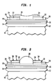
- FIG. 1 is a schematic side view of a portion of a component-mounting substrate that includes a deposited solder pattern overlying a bonding pad that includes a specific illustrative two-layer dam structure made in accordance with the principles of the present invention;
- FIG. 2 shows the FIG. 1 arrangement after the deposited solder has been flowed to form a solder bump;
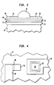
- FIG. 3 depicts the FIG. 2 structure after the top layer of the dam has been removed;
- FIG. 4 is a top view of a portion of the component represented in FIGS. 1 through 3;
- and FIG. 5 is a side view of the component depicted in FIG. 4, showing it solder bonded to another component.
- By way of a specific example, FIG. 1 shows a portion of a particular substrate on which a component (such as a laser device or an integrated-circuit chip) is designed to be mounted by solder bonding. Illustratively,
substrate 10 of FIG. 1 comprises a silicon wafer having a top surface covered by alayer 12 made of a suitable insulating material such as silicon dioxide. - By conventional techniques well known in the semiconductor processing art, metallization is deposited on the entire top surface of the
layer 12 and then patterned to form an array of bonding pads and interconnecting conductive lines. For illustrative purposes, a particular conventional four-layer metallization system will be assumed herein. This four-layer system comprises, for example, from bottom to top, layers of titanium, titanium nitride, platinum and gold. - Specifically, as depicted in FIG. 1, the
bottom-most layer 14 of the aforementioned metallization pattern comprises, for example, a layer of titanium having a Y-direction thickness of about 250-to-1000 Angstrom units. Thenext layer 16 comprises a layer of titanium nitride approximately 250 Angstrom units thick. Thethird layer 18 comprises a layer of platinum about 2000 Angstrom units thick. And the fourth ortop-most layer 20 of the illustrative metallization pattern comprises a layer of gold approximately 1000-to-10,000 Angstrom units thick. - The arrangement shown in FIG. 1 also includes a confinement or dam structure that in effect defines those areas of the metallization pattern on which solder bumps will be formed. In accordance with the principles of the present invention, the dam structure of FIG. 1 comprises two patterned
layers upper layer 24 is a sacrificial layer that is removed during subsequent processing. Thelower layer 22 remains on the depicted arrangement to serve as a dam during later processing steps. - The materials of the
layers bottom layer 22 is selected to be substantially unaffected by the process employed to remove thetop layer 24. Thus, for example, if thetop layer 24 is to be removed by etching (as described in detail later below), thebottom layer 22 is designed to be largely unaffected by the etching step. - Illustratively, the
bottom layer 22 of FIG. 1 comprises a layer of titanium nitride about 250-to-500 Angstrom units thick. Theupper layer 24 comprises, for example, a layer of chromium approximately 250-to-500 Angstrom units thick. - A variety of other materials that are not wetted by solder to any substantial extent are available for forming the
dam layers bottom layer 22 can be made of titanium nitride or silicon dioxide, while thetop layer 24 can be made of titanium, silicon nitride or aluminum oxide. In each case, the top layer of the two-layer dam structure is designed to be removable by a process that does not substantially affect the lower dam layer. - As a prelude to the formation of solder bumps, a solder pattern is defined on the FIG. 1 arrangement in conventional ways. The elements of this solder pattern are respectively defined overlying regions of the metallization that are confined by dam structures. One such
specific element 26 is represented in FIG. 1. - The portion of the solder element 26 (FIG. 1) that overlies the top non-wettable surface of the
dam layer 24 is substantially not adhered thereto. But thesolder element 26 is securely adhered to thetop-most layer 18 of the metallization confined within the depicted dam structure. Such attachment maintains theintegral solder element 26 securely in place. - Illustratively, the aforementioned solder pattern including the
element 26 of FIG. 1 is formed from a deposited (for example, a sputtered or an electron-beam-evaporated) layer about one-to-six micrometers (µm) thick. Various known solder formulations are suitable for this purpose. One such advantageous solder comprises a eutectic gold/tin mixture whose atomic percentage of gold to tin is about 70:30. Patterning such a thin-film layer of solder utilizing standard lithographic and lift-off techniques is straightforward. - During formation of the two-layer dam structure shown in FIG. 1, the top gold layer of the aforespecified illustrative metallization pattern is typically removed from the area directly underlying the dam. Furthermore, during deposition of the solder layer, the portion of the gold layer confined within the dam structure is dissolved by the solder. Thus, in the specific illustrative example described herein, the area directly below the dam as well as that directly below the area confined within the dam comprises a gold-less three-layer metallization, as indicated in FIG. 1.
- Subsequently, the FIG. 1 arrangement is processed to form solder bumps thereon. For the particular illustrative solder formulation specified above, this is accomplished, for example, by processing the arrangement in a reducing atmosphere at about 300 degrees Celsius for approximately five seconds. As a result of this step and due to surface-tension effects, the patterned solder elements (such as the
element 26 of FIG. 1) move off of the surface of thedam layer 24 and form domed bumps directly overlying the metallization confined within the dam structure, in a manner well known in the art. One such solder bump is shown in FIG. 2 wherein it is designated byreference numeral 28. Illustratively, the height of each such bump is approximately five-to-twenty-five µm. - Importantly, because of the blocking action of the indicated dam structure, the molten solder does not wick or flow to adjacent gold-layer areas during bump formation. As a result of this controlled confinement of solder, all of the solder bumps end up having substantially the same height, which is a required condition for reliable solder bonding.
- In practice, it has been observed that some randomly shaped and randomly positioned pieces of solder sometimes remain on the top surface of the dam after formation of the solder bumps. Several
such pieces - Because of the non-wettable nature of the surface of the top dam layer 24 (FIG. 2), the
solder pieces 30.32and 34 are not securely adhered to the surface of thelayer 24. Thus, these pieces, if not completely removed from the structure, can later move relatively easily from the indicated surface to other parts of the component assembly package. And, in so moving, this debris can, for example, cause electrical shorts, mechanical damage or optical interference in the final assembly. - In accordance with the principles of the present invention, all of the aforementioned solder debris is dislodged and removed from the indicated surface in an effective way. The manufacturing yield of high-reliability solder-bonded component assemblies is thereby significantly enhanced.
- In accordance with the invention, the debris-removal process comprises removing the top or
sacrificial layer 24 of the two-layer dam structure shown in FIG. 2. In the process of removing thelayer 24, thesolder pieces 30. 32 and 34 are also removed. At the same time, thebottom dam layer 22 is retained in place substantially intact. - Illustratively, the
top dam layer 24 of FIG. 2 is removed in an etching step. This is done by utilizing an etchant that dissolves thelayer 24 but which does not substantially attack the bottom layer 22 (or any other layers of the depicted structure). For the particular case in which thetop layer 24 is made of chromium. a suitable etchant therefor is, for example, a mixture of ceric ammonium nitrate, acetic acid and water, which is commercially available from Foto Chemical Systems, Inc., Wayne, New Jersey, as an etching solution designated C. A. N.. This solution is, for example, diluted 1:1 by volume with water prior to being used to etch thelayer 24. - Other suitable etchants for the
layer 24 are well known. Thus, for example, hydrochloric acid is effective to etch thelayer 24 without substantially attacking thelayer 22. - Even as the
layer 24 is dissolved by etching, the solder-debris pieces may get electrostatically charged and thereby may be difficult to disengage from the FIG. 2 structure. For this reason, it is generally advantageous to add a suitable surfactant to the etching solution to facilitate complete removal of solder debris from the indicated structure. One exemplary such surfactant comprises, for example, alkylaryl polyether alcohol, which, for example, is commercially available from J. T. Baker, Inc, Phillipsburg, New Jersey, as a surfactant designated Triton X-100. Illustratively, Triton X-100 is diluted with water (about 1:100 parts by volume) and then added to an etchant such as C. A. N. in a C. A. N.-to-Triton X-100 volume ratio of approximately 4:1. - Advantageously, while the FIG. 2 structure is contained in a vessel immersed in the etching-surfactant solution, the vessel is vibrated. This facilitates the etching process and removal of solder debris from the structure. For example, vibration at 5-to-50 Hertz with a conventional vibrator (such as a Syntron Jogger Model J-1 made by FMC Corp.) is effective to insure that the solder pieces are completely dislodged from the structure and end up in the solution separated from the FIG. 2 structure.
- Etching, while vibrating, in the aforespecified illustrative solution removes the
top dam layer 24 of FIG. 2 while leaving thebottom dam layer 22 substantially intact. By this illustrative technique, adam layer 24 comprising a 1000-Angstrom-unit-thick layer of chromium is removed in, for example, about five minutes. - After removing the structure from the etching bath, it is advantageous to wash the structure in, for example, deionized water. After being dried, the structure is then ready for subsequent processing in a standard solder-bonding operation.
- FIG. 3 shows the herein-described structure after the
top dam layer 24 and thesolder pieces bottom layer 22 of the original two-layer dam structure remains intact. Thus, when the solder bumps (such as thebump 28 of FIG. 3) are subsequently heated to effect electrical and mechanical bonds between the depicted structure and bonding pads on an associated component, thelayer 22 is effective to block molten solder from flowing to adjacent gold areas of the metallization pattern. - FIG. 4, which is a top view of a portion of a structure of the type depicted in FIGS. 1 through 3, shows the remaining
dam layer 22 surrounding thesolder bump 28. It is apparent that during a subsequent bonding operation thedam 22 is positioned to prevent molten solder from flowing to theadjacent gold area 20. - FIG. 4 also shows another
illustrative solder bump 36 adhered to an underlying bonding pad.Layer 38 of FIG. 4 constitutes the remaining layer of what was originally a two-layer dam structure. The top or sacrificial layer overlying thedam layer 38 was removed in the same processing step in which the aforedescribedsacrificial dam layer 24 was removed. The remainingdam layer 38 prevents molten solder from flowing to anadjacent gold area 40 during a subsequent bonding operation. (Note that, since no part of the metallization pattern extends to the right or above or below thesolder bump 36, theparticular dam layer 38 illustrated in FIG. 4 need extend only along the left-hand edge of thebump 36.) - During the actual solder-bonding operation, a component such as the one shown in FIG. 4 is designed to be connected to another component. This other component can, for example, simply be a device with electrical leads. In that case, each lead would be aligned with a respective one of the solder bumps shown in FIG. 4 and bonded thereto. Herein, however, for illustrative purposes, the other component will be assumed to be of the particular type of
component 42 which is represented in a simplified manner in FIG. 5. By way of a specific example, thecomponent 42 of FIG. 5 contains an array of spaced-apart conductive bonding pads schematically illustrated by thepads substrate 48. Dams (not shown in the simplified showing of FIG. 5) may be associated with thepads substrate 48 during the solder-bonding operation. Importantly, the pattern of bonding pads including thepads component 42 substantially exactly matches the pattern of bonding pads that includes the pads underlying the solder bumps 28 and 36 of FIG. 4. - With the domed solder bumps of FIG. 4 in contact with the
pads solder elements 50 and 52. After the heating step, the solder resolidifies, with the resolidified solder element 50 securely bonded to thelayer 18 and to thepad 46, while theresolidified solder element 52 is securely bonded to another portion of thelayer 18 and to thepad 44. Electrical and mechanical connections between the two depicted components are thereby established. - Finally, it is to be understood that the above-described techniques and materials are only illustrative of the principles of the present invention. In accordance with these principles, numerous modifications and alternatives may be devised by those skilled in the art without departing from the spirit and scope of the invention.
Claims (12)
- A method of solder bonding comprising the steps offorming a conductive metallization pattern, including bonding pads, on the surface of a component,forming a two-layer dam structure, including a top sacrificial layer and a bottom permanent layer, on each of said pads to define a portion of each pad to which solder is to be adhered, said dam structure being adapted to prevent molten solder from flowing from said defined pad portion to adjacent portions of the metallization pattern,forming respective solder bumps on said defined pad portions,removing the top sacrificial layer of said dam structure,and, while maintaining conductive elements of an associated component in respective contact with said solder bumps, heating said solder bumps to bond said respective elements to said defined pad portions.
- A method as in claim 1 wherein said removing step comprises etching said top sacrificial layer in a solution that dissolves said top layer but which does not dissolve said bottom permanent layer to any substantial extent.
- A method as in claim 2 wherein a surfactant is added to said etching solution.
- A method as in claim 3 wherein said removal step is carried out in a container that is vibrated during etching.
- A method as in claim 4 wherein said top sacrificial layer comprises chromium.
- A method as in claim 5 wherein said bottom permanent layer comprises titanium nitride.
- A method as in claim 6 wherein said etching solution comprises a mixture of ceric ammonium nitrate, acetic acid and water.
- A method as in claim 7 wherein said surfactant comprises alkylaryl polyether alcohol.
- A method as in claim 8 wherein said chromium layer is approximately 500-to-1000 Angstrom units thick.
- A method as in claim 9 wherein said titanium nitride layer is approximately 250-to-500 Angstrom units thick.
- A method as in claim 10 wherein said container is vibrated at 5-to-50 Hertz during the removal step.
- A method as in claim 11 wherein said solder comprises a eutectic gold/tin mixture.
Applications Claiming Priority (2)
| Application Number | Priority Date | Filing Date | Title |
|---|---|---|---|
| US08/490,878 US5620131A (en) | 1995-06-15 | 1995-06-15 | Method of solder bonding |
| US490878 | 1995-06-15 |
Publications (2)
| Publication Number | Publication Date |
|---|---|
| EP0749157A2 true EP0749157A2 (en) | 1996-12-18 |
| EP0749157A3 EP0749157A3 (en) | 1997-05-07 |
Family
ID=23949877
Family Applications (1)
| Application Number | Title | Priority Date | Filing Date |
|---|---|---|---|
| EP96304039A Withdrawn EP0749157A3 (en) | 1995-06-15 | 1996-06-04 | Method of solder bonding |
Country Status (4)
| Country | Link |
|---|---|
| US (1) | US5620131A (en) |
| EP (1) | EP0749157A3 (en) |
| JP (1) | JPH098082A (en) |
| KR (1) | KR970004992A (en) |
Cited By (2)
| Publication number | Priority date | Publication date | Assignee | Title |
|---|---|---|---|---|
| EP0961319A2 (en) * | 1998-05-28 | 1999-12-01 | Xerox Corporation | Integrated flexible interconnection |
| WO2017088998A1 (en) * | 2015-11-27 | 2017-06-01 | Snaptrack, Inc. | Electrical component with thin solder resist layer and method for the production thereof |
Families Citing this family (10)
| Publication number | Priority date | Publication date | Assignee | Title |
|---|---|---|---|---|
| DE19730118B4 (en) | 1997-07-14 | 2006-01-12 | Infineon Technologies Ag | Method and device for producing a chip-substrate connection |
| US5962151A (en) * | 1997-12-05 | 1999-10-05 | Delco Electronics Corp. | Method for controlling solderability of a conductor and conductor formed thereby |
| US6316736B1 (en) | 1998-06-08 | 2001-11-13 | Visteon Global Technologies, Inc. | Anti-bridging solder ball collection zones |
| US6378758B1 (en) * | 1999-01-19 | 2002-04-30 | Tessera, Inc. | Conductive leads with non-wettable surfaces |
| US6047637A (en) * | 1999-06-17 | 2000-04-11 | Fujitsu Limited | Method of paste printing using stencil and masking layer |
| US6427901B2 (en) * | 1999-06-30 | 2002-08-06 | Lucent Technologies Inc. | System and method for forming stable solder bonds |
| US6251732B1 (en) * | 1999-08-10 | 2001-06-26 | Macronix International Co., Ltd. | Method and apparatus for forming self-aligned code structures for semi conductor devices |
| US8802556B2 (en) * | 2012-11-14 | 2014-08-12 | Qualcomm Incorporated | Barrier layer on bump and non-wettable coating on trace |
| KR20210157787A (en) | 2020-06-22 | 2021-12-29 | 삼성전자주식회사 | Semiconductor package and method of fabricating the same |
| KR20220008088A (en) | 2020-07-13 | 2022-01-20 | 삼성전자주식회사 | Semiconductor package |
Citations (3)
| Publication number | Priority date | Publication date | Assignee | Title |
|---|---|---|---|---|
| JPH0252436A (en) * | 1988-08-17 | 1990-02-22 | Shimadzu Corp | Manufacture of solder bump |
| EP0358867A1 (en) * | 1988-07-15 | 1990-03-21 | Oerlikon-Contraves AG | Flip-chip mounting with a solder barrier layer made from oxidisable metal |
| US5162257A (en) * | 1991-09-13 | 1992-11-10 | Mcnc | Solder bump fabrication method |
Family Cites Families (4)
| Publication number | Priority date | Publication date | Assignee | Title |
|---|---|---|---|---|
| JPS5850021B2 (en) * | 1982-07-16 | 1983-11-08 | 富士通株式会社 | Manufacturing method for semiconductor devices |
| JPH05144815A (en) * | 1991-11-25 | 1993-06-11 | Ibiden Co Ltd | Substrate for mounting of electronic part with bump |
| KR960016007B1 (en) * | 1993-02-08 | 1996-11-25 | 삼성전자 주식회사 | Manufacturing method of semiconductor chip bump |
| US5536677A (en) * | 1994-12-01 | 1996-07-16 | Motorola, Inc. | Method of forming conductive bumps on a semiconductor device using a double mask structure |
-
1995
- 1995-06-15 US US08/490,878 patent/US5620131A/en not_active Expired - Lifetime
-
1996
- 1996-06-04 EP EP96304039A patent/EP0749157A3/en not_active Withdrawn
- 1996-06-14 JP JP8153654A patent/JPH098082A/en active Pending
- 1996-06-14 KR KR1019960021469A patent/KR970004992A/en not_active Application Discontinuation
Patent Citations (3)
| Publication number | Priority date | Publication date | Assignee | Title |
|---|---|---|---|---|
| EP0358867A1 (en) * | 1988-07-15 | 1990-03-21 | Oerlikon-Contraves AG | Flip-chip mounting with a solder barrier layer made from oxidisable metal |
| JPH0252436A (en) * | 1988-08-17 | 1990-02-22 | Shimadzu Corp | Manufacture of solder bump |
| US5162257A (en) * | 1991-09-13 | 1992-11-10 | Mcnc | Solder bump fabrication method |
Non-Patent Citations (2)
| Title |
|---|
| DATABASE WPI Week 199146, Derwent Publications Ltd., London, GB; AN 1991-337347, XP002905897 ANONYMOUS: 'Applying controlled solder amt. to circuit panel - using resist mask, strippable after solder reflowing' & RESEARCH DISCLOSURE vol. 330, no. 039, 01 October 1991, EMSWORTH, GB * |
| PATENT ABSTRACTS OF JAPAN vol. 007, no. 103 (E-173), 6 May 1983 & JP 58 025242 A (FUJITSU KK), 15 February 1983, * |
Cited By (4)
| Publication number | Priority date | Publication date | Assignee | Title |
|---|---|---|---|---|
| EP0961319A2 (en) * | 1998-05-28 | 1999-12-01 | Xerox Corporation | Integrated flexible interconnection |
| EP0961319A3 (en) * | 1998-05-28 | 2002-04-24 | Xerox Corporation | Integrated flexible interconnection |
| WO2017088998A1 (en) * | 2015-11-27 | 2017-06-01 | Snaptrack, Inc. | Electrical component with thin solder resist layer and method for the production thereof |
| CN108369935A (en) * | 2015-11-27 | 2018-08-03 | 追踪有限公司 | Electrical component with thin solder trapping layer and for the method for manufacture |
Also Published As
| Publication number | Publication date |
|---|---|
| KR970004992A (en) | 1997-01-29 |
| EP0749157A3 (en) | 1997-05-07 |
| JPH098082A (en) | 1997-01-10 |
| US5620131A (en) | 1997-04-15 |
Similar Documents
| Publication | Publication Date | Title |
|---|---|---|
| KR100509318B1 (en) | Solder bump structure and manufacturing method thereof | |
| US6713319B2 (en) | Method for fabricating a semiconductor apparatus including a sealing member with reduced thermal stress | |
| US5620131A (en) | Method of solder bonding | |
| JP3131379B2 (en) | Electronic module with multiple solder dams in the solder mask window | |
| US5466635A (en) | Process for making an interconnect bump for flip-chip integrated circuit including integral standoff and hourglass shaped solder coating | |
| EP0568995A2 (en) | Semiconductor device with bumps | |
| EP0357064A2 (en) | Metal bump type semiconductor device and method for manufacturing the same | |
| US5413964A (en) | Photo-definable template for semiconductor chip alignment | |
| KR100510543B1 (en) | Method for forming bump without surface defect | |
| JPH0689919A (en) | Electric internal connection substrate provided with both wire bond and solder connection and manufacture | |
| JP2006128625A (en) | Semiconductor device and its manufacturing method | |
| US7214604B2 (en) | Method of fabricating ultra thin flip-chip package | |
| JPH07201871A (en) | Method for forming metallic contact | |
| KR100562591B1 (en) | Method for the solder-stop structuring of elevations on wafers | |
| US6281445B1 (en) | Device and method for connecting two electronic components | |
| JPS62263645A (en) | Construction of electric contact and method of forming the same | |
| KR100790993B1 (en) | Flip chip having bump structure and method of manufacturing the same | |
| JPH0357223A (en) | Semiconductor device | |
| KR100233866B1 (en) | The structure of semiconductor chip for flip-chip and its manufacturing method | |
| JPH03139841A (en) | Structure of solder bump | |
| WO2023242185A1 (en) | Method for producing a semiconductor device and semiconductor device | |
| JP2528633B2 (en) | Semiconductor device | |
| KR20000025974A (en) | Method for forming solder bump comprising chromium under barrier metal | |
| JPH02172230A (en) | Method of forming electrode bump for connection | |
| JPH02232928A (en) | Solder bump structure of semiconductor chip |
Legal Events
| Date | Code | Title | Description |
|---|---|---|---|
| PUAI | Public reference made under article 153(3) epc to a published international application that has entered the european phase |
Free format text: ORIGINAL CODE: 0009012 |
|
| AK | Designated contracting states |
Kind code of ref document: A2 Designated state(s): DE FR GB |
|
| PUAL | Search report despatched |
Free format text: ORIGINAL CODE: 0009013 |
|
| AK | Designated contracting states |
Kind code of ref document: A3 Designated state(s): DE FR GB |
|
| 17P | Request for examination filed |
Effective date: 19971023 |
|
| 17Q | First examination report despatched |
Effective date: 19990702 |
|
| STAA | Information on the status of an ep patent application or granted ep patent |
Free format text: STATUS: THE APPLICATION IS DEEMED TO BE WITHDRAWN |
|
| 18D | Application deemed to be withdrawn |
Effective date: 20010104 |