EP0748507B1 - Anisotrop leitender kleber - Google Patents
Anisotrop leitender kleber Download PDFInfo
- Publication number
- EP0748507B1 EP0748507B1 EP95907559A EP95907559A EP0748507B1 EP 0748507 B1 EP0748507 B1 EP 0748507B1 EP 95907559 A EP95907559 A EP 95907559A EP 95907559 A EP95907559 A EP 95907559A EP 0748507 B1 EP0748507 B1 EP 0748507B1
- Authority
- EP
- European Patent Office
- Prior art keywords
- adhesive
- ligands
- conductor tracks
- particles
- adhesive according
- Prior art date
- Legal status (The legal status is an assumption and is not a legal conclusion. Google has not performed a legal analysis and makes no representation as to the accuracy of the status listed.)
- Expired - Lifetime
Links
Images
Classifications
-
- C—CHEMISTRY; METALLURGY
- C09—DYES; PAINTS; POLISHES; NATURAL RESINS; ADHESIVES; COMPOSITIONS NOT OTHERWISE PROVIDED FOR; APPLICATIONS OF MATERIALS NOT OTHERWISE PROVIDED FOR
- C09J—ADHESIVES; NON-MECHANICAL ASPECTS OF ADHESIVE PROCESSES IN GENERAL; ADHESIVE PROCESSES NOT PROVIDED FOR ELSEWHERE; USE OF MATERIALS AS ADHESIVES
- C09J9/00—Adhesives characterised by their physical nature or the effects produced, e.g. glue sticks
- C09J9/02—Electrically-conducting adhesives
-
- H—ELECTRICITY
- H01—ELECTRIC ELEMENTS
- H01B—CABLES; CONDUCTORS; INSULATORS; SELECTION OF MATERIALS FOR THEIR CONDUCTIVE, INSULATING OR DIELECTRIC PROPERTIES
- H01B1/00—Conductors or conductive bodies characterised by the conductive materials; Selection of materials as conductors
- H01B1/20—Conductive material dispersed in non-conductive organic material
- H01B1/22—Conductive material dispersed in non-conductive organic material the conductive material comprising metals or alloys
-
- H—ELECTRICITY
- H01—ELECTRIC ELEMENTS
- H01R—ELECTRICALLY-CONDUCTIVE CONNECTIONS; STRUCTURAL ASSOCIATIONS OF A PLURALITY OF MUTUALLY-INSULATED ELECTRICAL CONNECTING ELEMENTS; COUPLING DEVICES; CURRENT COLLECTORS
- H01R4/00—Electrically-conductive connections between two or more conductive members in direct contact, i.e. touching one another; Means for effecting or maintaining such contact; Electrically-conductive connections having two or more spaced connecting locations for conductors and using contact members penetrating insulation
- H01R4/04—Electrically-conductive connections between two or more conductive members in direct contact, i.e. touching one another; Means for effecting or maintaining such contact; Electrically-conductive connections having two or more spaced connecting locations for conductors and using contact members penetrating insulation using electrically conductive adhesives
-
- H—ELECTRICITY
- H05—ELECTRIC TECHNIQUES NOT OTHERWISE PROVIDED FOR
- H05K—PRINTED CIRCUITS; CASINGS OR CONSTRUCTIONAL DETAILS OF ELECTRIC APPARATUS; MANUFACTURE OF ASSEMBLAGES OF ELECTRICAL COMPONENTS
- H05K3/00—Apparatus or processes for manufacturing printed circuits
- H05K3/30—Assembling printed circuits with electric components, e.g. with resistors
- H05K3/32—Assembling printed circuits with electric components, e.g. with resistors electrically connecting electric components or wires to printed circuits
- H05K3/321—Assembling printed circuits with electric components, e.g. with resistors electrically connecting electric components or wires to printed circuits by conductive adhesives
- H05K3/323—Assembling printed circuits with electric components, e.g. with resistors electrically connecting electric components or wires to printed circuits by conductive adhesives by applying an anisotropic conductive adhesive layer over an array of pads
-
- H—ELECTRICITY
- H05—ELECTRIC TECHNIQUES NOT OTHERWISE PROVIDED FOR
- H05K—PRINTED CIRCUITS; CASINGS OR CONSTRUCTIONAL DETAILS OF ELECTRIC APPARATUS; MANUFACTURE OF ASSEMBLAGES OF ELECTRICAL COMPONENTS
- H05K2201/00—Indexing scheme relating to printed circuits covered by H05K1/00
- H05K2201/02—Fillers; Particles; Fibers; Reinforcement materials
- H05K2201/0203—Fillers and particles
- H05K2201/0206—Materials
- H05K2201/0224—Conductive particles having an insulating coating
-
- H—ELECTRICITY
- H05—ELECTRIC TECHNIQUES NOT OTHERWISE PROVIDED FOR
- H05K—PRINTED CIRCUITS; CASINGS OR CONSTRUCTIONAL DETAILS OF ELECTRIC APPARATUS; MANUFACTURE OF ASSEMBLAGES OF ELECTRICAL COMPONENTS
- H05K2203/00—Indexing scheme relating to apparatus or processes for manufacturing printed circuits covered by H05K3/00
- H05K2203/11—Treatments characterised by their effect, e.g. heating, cooling, roughening
- H05K2203/1163—Chemical reaction, e.g. heating solder by exothermic reaction
-
- H—ELECTRICITY
- H05—ELECTRIC TECHNIQUES NOT OTHERWISE PROVIDED FOR
- H05K—PRINTED CIRCUITS; CASINGS OR CONSTRUCTIONAL DETAILS OF ELECTRIC APPARATUS; MANUFACTURE OF ASSEMBLAGES OF ELECTRICAL COMPONENTS
- H05K2203/00—Indexing scheme relating to apparatus or processes for manufacturing printed circuits covered by H05K3/00
- H05K2203/12—Using specific substances
- H05K2203/121—Metallo-organic compounds
Definitions
- the invention relates to an anisotropically conductive Adhesive according to the preamble of claim 1.
- Anisotropically conductive adhesives are known. These point in a base material, for example in a thermoplastic material, finely divided conductive Particles on. The conductive particles will thereby as a granular powder in the base material dispersed.
- the anisotropically conductive adhesive are, for example, in foil form and are suitable for two contacts, for example two Conductor tracks, electrically conductive to each other glue.
- the conductor tracks are under pressure and Effect of temperature on the opposite Sides of the conductive adhesive pressed so that the Base material deformed and the distributed in this conductive particles an electrically conductive connection between the applied conductor tracks produce.
- the base material takes over the Adhesive effect for the conductor tracks.
- anisotropic conductive adhesive that is the minimum possible Distance between two adjacent electrically conductive Compounds, from the structure of the dispersed depends on electrically conductive particles. So that the electrically conductive connection in enable only one direction, these must be one have a sufficient distance from each other so that an undesirable electrically conductive connection between the particles is avoided.
- the anisotropically conductive adhesive according to the invention with has the features mentioned in claim 1 the advantage that a uniform dispersion of the conductive particles in the base material is possible. Because the conductive Particles have spacers on their surface, coagulation of the particles is avoided. These are therefore evenly dispersed in the base material without the particles are electrically connected to each other. This has the advantage that the minimum Distance between two adjacent contact connections in itself only of a grain size of electrically conductive particles is determined. The Anisotropy of the contact connection is thereby high security guaranteed.
- that the spacer has a coating are from ligands, which are preferably not thermally are stable. This ensures that the electrical conductive particles through the ligands in an unprocessed conductive adhesive kept at a distance become. Because the ligands are thermal are not stable, they are and contact process and can thus the manufacture of an electrically conductive Don't hinder connection. The dissolution of the Ligands only occur at a time when the and connection process in which the electrical conductive particles already under a certain Are under pressure so that despite the elimination of the Spacers no longer in contact with each other can come.
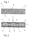
- Figure 1 shows one in foil form anisotropically conductive adhesive 10.
- the adhesive 10 consists of a base material 12 and therein dispersed, i.e. finely divided, conductive Particles 14.
- the base material 12 is made of it for example from a thermoset or Thermoplastic.
- the particles 14 can, for example made of gold, nickel, gold-plated nickel, silver or gold-coated styrofoam balls.
- the Particles 14 are provided with a coating 16, which is not indicated to scale in FIG. 1 is.
- the coating 16 is there for example from triphenylphosphine.
- Figure 2 shows a possibility of a glued connection with the adhesive shown in Figure 1.
- Adhesive 10 On the opposite surfaces of the Adhesive 10, conductor tracks 18 and 20 are applied. The conductor tracks 18 and 20 are located still on the adhesive 10 and are not in this penetrated. For example, over the conductor tracks 18 a film 22 made of polyester or polyamide upset. The conductor tracks 20 are also covered with a film 24. The slides 22 and 24 can be part of a electronic component that the conductor tracks 18 or 20.
- adhesive 10 takes place as follows. On that from the adhesive 10 with the applied conductor tracks 18 and 20 as well as the slides 22 and 24 existing System is shown with a stamp, in Figure 2 indicated by the arrow, pressure applied. At the same time, the system heats up. Due to the heating, the thermoplastic becomes existing base material 12 softened so that the Conductor tracks 18 and 20 under the pressure of the stamp can penetrate into the base material 12. While the coating 16 decomposes when heated Triphenylphosphine as this has a decomposition temperature 60 ° C, while the base material 12 to a temperature of approx. 150 to 230 ° C is heated.
- the coating 16 By decomposing the coating 16 can the conductor tracks 18 and 20 so be pressed far to the particles 14 that between the particles 14 and the conductor tracks 18 or 20 an electrically conductive connection is formed. After the system has hardened, for example in a time of 5 to 30 seconds, the stamp can be removed and the conductor tracks 18 and 20 are constantly electrical with each other contacted. Because the electrical Connection only from between the conductor tracks 18 and 20 particles 14 Adjacent contacts can be used between conductor tracks 18 and 20 confined space can be realized without it Misconnections via touching particles 14 is coming. Overall, this means a higher resolution between adjacent conductor tracks 18 and 20 possible. The total contact connection is therefore very safe. Can be very beneficial with the anisotropic shown in Figures 1 and 2 conductive adhesive 10 flexible connections between produce the conductor tracks 18 and 20. The The flexibility of the connection only depends from the base material 12.
- Adhesive 10 can also be used, for example, as a paste or film or heat sealing film.
- the connecting of two conductor tracks 18 and 20 only as the simplest embodiment to understand.
- Via appropriately structured Stamps can, for example, be on the surface of an adhesive 10 distributed different vias are produced depending on the Use case are variable.
Landscapes
- Chemical & Material Sciences (AREA)
- Engineering & Computer Science (AREA)
- Organic Chemistry (AREA)
- Physics & Mathematics (AREA)
- Dispersion Chemistry (AREA)
- Spectroscopy & Molecular Physics (AREA)
- Manufacturing & Machinery (AREA)
- Microelectronics & Electronic Packaging (AREA)
- Adhesives Or Adhesive Processes (AREA)
- Conductive Materials (AREA)
- Connections Effected By Soldering, Adhesion, Or Permanent Deformation (AREA)
Abstract
Description
- Figur 1
- eine Schnittdarstellung durch einen anisotrop leitenden Kleber im Ausgangszustand und
- Figur 2
- eine Schnittdarstellung durch einen anisotrop leitenden Kleber im kontaktierten Zustand.
Claims (9)
- Anisotrop leitender Kleber mit in einem Basismaterial dispergierten leitfähigen Teilchen, dadurch gekennzeichnet, daß die Teilchen (14) auf ihrer Oberfläche als Abstandsmittel Liganden aufweisen, die sich während eines Klebeprozesses zersetzen.
- Kleber nach Anspruch 1, dadurch gekennzeichnet, daß die Liganden thermisch nicht stabil sind.
- Kleber nach einem der vorhergehenden Ansprüche, dadurch gekennzeichnet, daß die Liganden eine zersetzungstemperatur besitzen, die unterhalb einer Verklebetemperatur liegt.
- Kleber nach einem der vorhergehenden Ansprüche, dadurch gekennzeichnet, daß als Ligand Triphenylphosphin verwendet wird.
- Kleber nach einem der vorhergehenden Ansprüche, dadurch gekennzeichnet, daß als Ligand Propionsäure verwendet wird.
- Kleber nach einem der vorhergehenden Ansprüche, dadurch gekennzeichnet, daß die Teilchen (14) aus Gold, Nickel, vergoldetem Nickel, Silber oder goldbeschichteten Styroporkugeln bestehen.
- Kleber nach einem der vorhergehenden Ansprüche, dadurch gekennzeichnet, daß das Basismaterial aus einem Duroplast oder einem Thermoplast besteht.
- Verfahren zur Herstellung einer geklebten, elektrisch leitfähigen Verbindung zwischen Leiterbahnen, dadurch gekennzeichnet, daß die Leiterbahnen auf sich gegenüberliegenden Oberflächen eines Klebers nach einem der Patentansprüche 1 bis 7 aufgebracht werden, auf den Kleber und die Leiterbahnen Druck ausgeübt wird und die im Kleber enthaltenen Liganden zersetzt werden.
- Verfahren nach Anspruch 8, dadurch gekennzeichnet, daß die Liganden unter Erwärmung zersetzt werden.
Applications Claiming Priority (3)
| Application Number | Priority Date | Filing Date | Title |
|---|---|---|---|
| DE4406418 | 1994-02-28 | ||
| DE4406418A DE4406418C1 (de) | 1994-02-28 | 1994-02-28 | Anisotrop elektrisch leitender Kleber |
| PCT/DE1995/000151 WO1995023416A1 (de) | 1994-02-28 | 1995-02-07 | Anisotrop leitender kleber |
Publications (2)
| Publication Number | Publication Date |
|---|---|
| EP0748507A1 EP0748507A1 (de) | 1996-12-18 |
| EP0748507B1 true EP0748507B1 (de) | 1999-06-16 |
Family
ID=6511361
Family Applications (1)
| Application Number | Title | Priority Date | Filing Date |
|---|---|---|---|
| EP95907559A Expired - Lifetime EP0748507B1 (de) | 1994-02-28 | 1995-02-07 | Anisotrop leitender kleber |
Country Status (5)
| Country | Link |
|---|---|
| US (1) | US5891365A (de) |
| EP (1) | EP0748507B1 (de) |
| JP (1) | JPH09509280A (de) |
| DE (2) | DE4406418C1 (de) |
| WO (1) | WO1995023416A1 (de) |
Cited By (1)
| Publication number | Priority date | Publication date | Assignee | Title |
|---|---|---|---|---|
| DE102010002447A1 (de) | 2010-02-26 | 2011-09-01 | Tutech Innovation Gmbh | Klebstoff mit anisotroper elektrischer Leitfähigkeit sowie Verfahren zu dessen Herstellung und Verwendung |
Families Citing this family (5)
| Publication number | Priority date | Publication date | Assignee | Title |
|---|---|---|---|---|
| DE19632814A1 (de) * | 1996-08-14 | 1998-02-19 | Siemens Ag | Kombikarte und Verfahren zu ihrer Herstellung |
| DE19636813C1 (de) * | 1996-09-11 | 1998-01-29 | Bosch Gmbh Robert | Verfahren zur Montage von Piezoelementen auf Oberflächen |
| US6802446B2 (en) * | 2002-02-01 | 2004-10-12 | Delphi Technologies, Inc. | Conductive adhesive material with metallurgically-bonded conductive particles |
| DE10204959A1 (de) * | 2002-02-06 | 2003-08-14 | Endress & Hauser Gmbh & Co Kg | Leiterplatte mit einem Bauteil |
| DE102018219879B4 (de) | 2018-11-20 | 2022-10-06 | Danfoss Silicon Power Gmbh | Elektrische verbindungsanordnung |
Family Cites Families (8)
| Publication number | Priority date | Publication date | Assignee | Title |
|---|---|---|---|---|
| GB1477780A (en) * | 1974-08-14 | 1977-06-29 | Seikosha Kk | Assembly incorporating electrically conductive adhesive |
| AU572615B2 (en) * | 1983-12-27 | 1988-05-12 | Sony Corporation | Electrically conductive adhesive sheet circuit board and electrical connection structure |
| JPS6433808A (en) * | 1986-10-18 | 1989-02-03 | Japan Synthetic Rubber Co Ltd | Conductive particle and conductive adhesive including it |
| US4999460A (en) * | 1989-08-10 | 1991-03-12 | Casio Computer Co., Ltd. | Conductive connecting structure |
| US5376403A (en) * | 1990-02-09 | 1994-12-27 | Capote; Miguel A. | Electrically conductive compositions and methods for the preparation and use thereof |
| JPH0450256A (ja) * | 1990-06-18 | 1992-02-19 | Mitsubishi Electric Corp | エポキシ樹脂組成物およびその製法 |
| JPH04115407A (ja) * | 1990-09-03 | 1992-04-16 | Soken Kagaku Kk | 異方導電性接着剤組成物 |
| US5136365A (en) * | 1990-09-27 | 1992-08-04 | Motorola, Inc. | Anisotropic conductive adhesive and encapsulant material |
-
1994
- 1994-02-28 DE DE4406418A patent/DE4406418C1/de not_active Expired - Fee Related
-
1995
- 1995-02-07 US US08/676,292 patent/US5891365A/en not_active Expired - Fee Related
- 1995-02-07 DE DE59506240T patent/DE59506240D1/de not_active Expired - Fee Related
- 1995-02-07 EP EP95907559A patent/EP0748507B1/de not_active Expired - Lifetime
- 1995-02-07 WO PCT/DE1995/000151 patent/WO1995023416A1/de not_active Ceased
- 1995-02-07 JP JP7522054A patent/JPH09509280A/ja active Pending
Cited By (2)
| Publication number | Priority date | Publication date | Assignee | Title |
|---|---|---|---|---|
| DE102010002447A1 (de) | 2010-02-26 | 2011-09-01 | Tutech Innovation Gmbh | Klebstoff mit anisotroper elektrischer Leitfähigkeit sowie Verfahren zu dessen Herstellung und Verwendung |
| WO2011104370A1 (de) | 2010-02-26 | 2011-09-01 | Tutech Innovation Gmbh | Klebstoff mit anisotroper elektrischer leitfähigkeit sowie verfahren zu dessen herstellung und verwendung |
Also Published As
| Publication number | Publication date |
|---|---|
| WO1995023416A1 (de) | 1995-08-31 |
| DE4406418C1 (de) | 1995-07-13 |
| DE59506240D1 (de) | 1999-07-22 |
| JPH09509280A (ja) | 1997-09-16 |
| EP0748507A1 (de) | 1996-12-18 |
| US5891365A (en) | 1999-04-06 |
Similar Documents
| Publication | Publication Date | Title |
|---|---|---|
| DE4301692C2 (de) | Verfahren zum elektrischen Verbinden von auf einer ersten und zweiten Isohörplatte angeordneten Leiterbahnen | |
| DE2820403C2 (de) | Verfahren zum Ankleben und zum Kontaktieren eines elektrischen Bauteils mit einer flächenförmigen Elektrode | |
| DE3787987T2 (de) | Anisotropisches elastomeres Zwischenverbindungssystem. | |
| EP0767964B1 (de) | Anisotrop leitender kleber und verfahren zur herstellung eines anisotrop leitenden klebers | |
| DE9114141U1 (de) | Elektrischer Verbinder mit leitfähigem Gel | |
| DE3904827A1 (de) | Elektrischer steckverbinder | |
| EP0757330A2 (de) | Verfahren zur Herstellung eines Datenträgers | |
| DE102008018199A1 (de) | Elektrische Baugruppe mit einem Stanzgitter, elektrischen Bauelementen und einer Füllmasse | |
| DE4406418C1 (de) | Anisotrop elektrisch leitender Kleber | |
| DE69317180T2 (de) | Verfahren zur Herstellung von IC-Karten | |
| EP0215385A1 (de) | Verfahren und Vorrichtung zum Verbinden von Platten durch Stanznocken | |
| CH646280A5 (de) | Verfahren zur herstellung von verbindungszwischenstuecken. | |
| DE2523361C3 (de) | Elektrischer Steckverbinder und Verfahren zur Herstellung desselben | |
| DE102017208253A1 (de) | Verfahren zum Herstellen eines PTC-Heizelementes | |
| EP0512124B1 (de) | Tastatur | |
| DE19510186A1 (de) | Verfahren zum Anschluß eines flexiblen Verbindungselements an ein Substrat | |
| EP0998723B1 (de) | Modul und seine verwendung in einer chipkarte | |
| DE3247574A1 (de) | Verfahren zum herstellen einer anordnung zur signalerzeugung | |
| DE19517062A1 (de) | Anisotrop leitender Kleber und Verfahren zur Herstellung eines anisotrop leitenden Klebers | |
| DE69407016T2 (de) | Klemmvorrichtung für elektrischen Anschluss | |
| WO1999038368A1 (de) | Verfahren zur herstellung eines ein elektronikbauteil enthaltenden kunststoffobjektes | |
| DE2206401B2 (de) | Steckverbinder | |
| DE2319926A1 (de) | Schweiss- und schneidvorrichtung | |
| DE1690542A1 (de) | Verfahren zur mechanischen Separierung reproduzierbarer,diskreter Leiterbahnen auf mit leitender Schicht bedecktem Isoliermaterial | |
| DE10323842B3 (de) | Verfahren zum Herstellen einer Chipanordnung und Lack mit ferromagnetischen Partikeln |
Legal Events
| Date | Code | Title | Description |
|---|---|---|---|
| PUAI | Public reference made under article 153(3) epc to a published international application that has entered the european phase |
Free format text: ORIGINAL CODE: 0009012 |
|
| 17P | Request for examination filed |
Effective date: 19960930 |
|
| AK | Designated contracting states |
Kind code of ref document: A1 Designated state(s): DE FR GB IT |
|
| GRAG | Despatch of communication of intention to grant |
Free format text: ORIGINAL CODE: EPIDOS AGRA |
|
| 17Q | First examination report despatched |
Effective date: 19980915 |
|
| GRAG | Despatch of communication of intention to grant |
Free format text: ORIGINAL CODE: EPIDOS AGRA |
|
| GRAH | Despatch of communication of intention to grant a patent |
Free format text: ORIGINAL CODE: EPIDOS IGRA |
|
| GRAH | Despatch of communication of intention to grant a patent |
Free format text: ORIGINAL CODE: EPIDOS IGRA |
|
| GRAA | (expected) grant |
Free format text: ORIGINAL CODE: 0009210 |
|
| AK | Designated contracting states |
Kind code of ref document: B1 Designated state(s): DE FR GB IT |
|
| REF | Corresponds to: |
Ref document number: 59506240 Country of ref document: DE Date of ref document: 19990722 |
|
| ET | Fr: translation filed | ||
| ITF | It: translation for a ep patent filed | ||
| GBT | Gb: translation of ep patent filed (gb section 77(6)(a)/1977) |
Effective date: 19990825 |
|
| PGFP | Annual fee paid to national office [announced via postgrant information from national office to epo] |
Ref country code: DE Payment date: 19991230 Year of fee payment: 6 |
|
| PGFP | Annual fee paid to national office [announced via postgrant information from national office to epo] |
Ref country code: GB Payment date: 20000125 Year of fee payment: 6 |
|
| PGFP | Annual fee paid to national office [announced via postgrant information from national office to epo] |
Ref country code: FR Payment date: 20000222 Year of fee payment: 6 |
|
| PLBE | No opposition filed within time limit |
Free format text: ORIGINAL CODE: 0009261 |
|
| STAA | Information on the status of an ep patent application or granted ep patent |
Free format text: STATUS: NO OPPOSITION FILED WITHIN TIME LIMIT |
|
| 26N | No opposition filed | ||
| PG25 | Lapsed in a contracting state [announced via postgrant information from national office to epo] |
Ref country code: GB Free format text: LAPSE BECAUSE OF NON-PAYMENT OF DUE FEES Effective date: 20010207 |
|
| GBPC | Gb: european patent ceased through non-payment of renewal fee |
Effective date: 20010207 |
|
| PG25 | Lapsed in a contracting state [announced via postgrant information from national office to epo] |
Ref country code: FR Free format text: LAPSE BECAUSE OF NON-PAYMENT OF DUE FEES Effective date: 20011031 |
|
| REG | Reference to a national code |
Ref country code: FR Ref legal event code: ST |
|
| PG25 | Lapsed in a contracting state [announced via postgrant information from national office to epo] |
Ref country code: DE Free format text: LAPSE BECAUSE OF NON-PAYMENT OF DUE FEES Effective date: 20011201 |
|
| PG25 | Lapsed in a contracting state [announced via postgrant information from national office to epo] |
Ref country code: IT Free format text: LAPSE BECAUSE OF NON-PAYMENT OF DUE FEES;WARNING: LAPSES OF ITALIAN PATENTS WITH EFFECTIVE DATE BEFORE 2007 MAY HAVE OCCURRED AT ANY TIME BEFORE 2007. THE CORRECT EFFECTIVE DATE MAY BE DIFFERENT FROM THE ONE RECORDED. Effective date: 20050207 |