EP0746014A2 - Trockenätzverfahren - Google Patents
Trockenätzverfahren Download PDFInfo
- Publication number
- EP0746014A2 EP0746014A2 EP96303886A EP96303886A EP0746014A2 EP 0746014 A2 EP0746014 A2 EP 0746014A2 EP 96303886 A EP96303886 A EP 96303886A EP 96303886 A EP96303886 A EP 96303886A EP 0746014 A2 EP0746014 A2 EP 0746014A2
- Authority
- EP
- European Patent Office
- Prior art keywords
- etching
- dry
- silicon
- solid surface
- solid
- Prior art date
- Legal status (The legal status is an assumption and is not a legal conclusion. Google has not performed a legal analysis and makes no representation as to the accuracy of the status listed.)
- Granted
Links
Images
Classifications
-
- H10P50/246—
-
- H—ELECTRICITY
- H01—ELECTRIC ELEMENTS
- H01L—SEMICONDUCTOR DEVICES NOT COVERED BY CLASS H10
- H01L21/00—Processes or apparatus adapted for the manufacture or treatment of semiconductor or solid state devices or of parts thereof
- H01L21/02—Manufacture or treatment of semiconductor devices or of parts thereof
- H01L21/04—Manufacture or treatment of semiconductor devices or of parts thereof the devices having potential barriers, e.g. a PN junction, depletion layer or carrier concentration layer
- H01L21/18—Manufacture or treatment of semiconductor devices or of parts thereof the devices having potential barriers, e.g. a PN junction, depletion layer or carrier concentration layer the devices having semiconductor bodies comprising elements of Group IV of the Periodic Table or AIIIBV compounds with or without impurities, e.g. doping materials
- H01L21/30—Treatment of semiconductor bodies using processes or apparatus not provided for in groups H01L21/20 - H01L21/26
- H01L21/302—Treatment of semiconductor bodies using processes or apparatus not provided for in groups H01L21/20 - H01L21/26 to change their surface-physical characteristics or shape, e.g. etching, polishing, cutting
- H01L21/306—Chemical or electrical treatment, e.g. electrolytic etching
- H01L21/30604—Chemical etching
- H01L21/30612—Etching of AIIIBV compounds
- H01L21/30621—Vapour phase etching
-
- H—ELECTRICITY
- H01—ELECTRIC ELEMENTS
- H01L—SEMICONDUCTOR DEVICES NOT COVERED BY CLASS H10
- H01L21/00—Processes or apparatus adapted for the manufacture or treatment of semiconductor or solid state devices or of parts thereof
- H01L21/02—Manufacture or treatment of semiconductor devices or of parts thereof
- H01L21/04—Manufacture or treatment of semiconductor devices or of parts thereof the devices having potential barriers, e.g. a PN junction, depletion layer or carrier concentration layer
- H01L21/18—Manufacture or treatment of semiconductor devices or of parts thereof the devices having potential barriers, e.g. a PN junction, depletion layer or carrier concentration layer the devices having semiconductor bodies comprising elements of Group IV of the Periodic Table or AIIIBV compounds with or without impurities, e.g. doping materials
- H01L21/30—Treatment of semiconductor bodies using processes or apparatus not provided for in groups H01L21/20 - H01L21/26
- H01L21/302—Treatment of semiconductor bodies using processes or apparatus not provided for in groups H01L21/20 - H01L21/26 to change their surface-physical characteristics or shape, e.g. etching, polishing, cutting
- H01L21/306—Chemical or electrical treatment, e.g. electrolytic etching
- H01L21/3065—Plasma etching; Reactive-ion etching
-
- H10P50/242—
Definitions
- the present invention relates to a method for dry-etching. More particularly, the present invention relates to a novel method for dry-etching a solid surface such as a silicon surface or a gallium arsenide surface, which is useful as a basic technology for the manufacture of quantum devices.
- the present invention was developed in view of the circumstances as described above, and has an object to provide a novel method for etching, which overcomes the restrictions in the conventional etching technique of solid surface, permits dry-etching at a high reproducibility by simple means also for an oxide film on a crystal surface, and allows achievement of a perfect dry-process.
- the present invention provides, as means to solve the above-mentioned problems, a method for dry-etching a solid surface with a gaseous bismuth halide compound.
- the present invention provides also methods for dry-ething with a gaseous bismuth halide compound which permits:
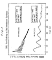
- Fig. 1 shows a diagram illustrating the relation between RHEED specular beam intensity and time in case of dry-etching Si(111) surface and GaAs (100) surface by BiF 3 .
- the present invention provides a method for dry-etching a solid surface simply at a high reproducibility by using a gaseous halide compound of bismuth (Bi) as described above in ultra high vacuum (UHV).
- the silicon surface is generally very rich in reactivity. As a result, this is considered a cause of contamination by impurities since different substances present on the surface are incorporated to reduce the large surface energy. Particularly during growth, removal of these impurities is an important task.
- surfactant means that positively utilizes this property to actively control surface energy is called "surfactant.” This is observed in all materials, and As and Sb are reported to be effective on silicon. However, the purpose in this case is to facilitate hetero-epitaxy into an unmatched lattice system (alleviating distortion to uniform state), incorporation of the surfactant itself into the film is very large.
- Bi is characterized in that, although it falls under the V family like As and Sb, the large atom radius permits remarkable inhibition of incorporation into the film. Furthermore, findings were obtained that heating to 400°C caused desorption of Bi from the surface. With these findings in view, possibility of using Bi as a carrier carrying halogen atoms to the surface was considered from the point of view of etching.
- the halide of bismuth (Bi) used as an etchant in the method of the present invention is expressed by a general formula BiX 3 (where X is a halogen atom and n is an integer), and can be selected from the group consisting of various compounds including those based on BiF 3 , BiCl 3 and BiBr 3 . Apart from halogen atoms, oxygen or sulfur atoms may be bonded. In all cases, these bismuth halides would be applied onto the solid surface.
- the method of present invention using a gaseous bismuth halide compound as an etchant realizes to etch an atom of surface in units of single atom or single atomic layer. Solid surface is etched in a atomic layer-by-layer fashion with bismuth halide compound.
- an etching accuracy is controlled within units of single atomic layer. Namely, the etching process is stopped at a desirable single atomic layer in accordance with a intensity of RHEED.
- the etching process is controlled by stopping a suply of a gaseous bismuth halide compound.
- K-cell is preferably used for controlling suply of bismuth halide compound by closing a shutter of the K-cell or opening said the shutter.
- the ultra high vacuum (UHV) condition is adopted.
- this ultra high vacuum (UHV) condition required by the dry-process and various other conditions for introduction and discharge of an etchant gas and heating of the substrate largely vary in accordance with the corresponding conventional methods within the scope of the present invention.
- BiF 3 was supplied as an etchant to Si(l11) and a surface oxide film was removed by dry-etching. By heating the etching-treated surface, there was available a clean and flat silicon surface. Subsequently, this clean surface was etched in a layer-by-layer fashion with BiF 3 ; about ten layers of oscillation of reflection high energy electron -diffraction (RHEED) representing etching in units of single atomic layer were observed. Residual Bi on the surface could be removed by heating the surface to about 400°C. Because, without irradiation of BiF 3 under the same conditions, no RHEED pattern is observed, BiF 3 is considered to remove the oxide film on the Si surface.
- RHEED reflection high energy electron -diffraction
- etching rate (ER) is therefore considered to be: ER(100) > ER(111) This is attributable to the fact that the supply rate limited range for the decomposition of BiF 3 is not reached on Si surface even 730°C, and the decomposition rate limited range has kept yet.
- the Si(100) plane has a larger number of dangling bonds. Reactivity of the surface is considered to be simply proportional to this number.
- Fig. 1 shows a diagram illustrating the relation between RHEED specular beam intensity and time for etching Si and GaAs in units of single atomic layer.
- the period of this oscillation corresponds to etching of single layer [double layer (a coupled single layer at Si(111)), a coupled GaAs single layer at GaAs(100)].
- double layer a coupled single layer at Si(111)
- ER was investigated from observation of RHEED oscillation on the GaAs(100) plane, the supply rate limited range was almost satisfied on GaAs at a substrate temperature of 500°C.
- decomposition of BiF 3 therefore, exchange of electrons with the substrate is very important: the difference in this catalyst-like function (i.e., between the GaAs substrate and the Si substrate) represents a large difference in ER (>50).
- growth of GaAs on Si is now a subject of active discussion. The selective etching would therefore become an important technology.
- Si layers Si as a dopant
- the present method realizes to etch both of GaAs and Si.
- AlAs was etched with a simillar etching rate (ER) of Si case. Then, the present method is also used for etching AlAs on GaAs.
- ER simillar etching rate
Landscapes
- Engineering & Computer Science (AREA)
- Physics & Mathematics (AREA)
- Computer Hardware Design (AREA)
- Condensed Matter Physics & Semiconductors (AREA)
- General Physics & Mathematics (AREA)
- Manufacturing & Machinery (AREA)
- Microelectronics & Electronic Packaging (AREA)
- Power Engineering (AREA)
- Plasma & Fusion (AREA)
- Chemical & Material Sciences (AREA)
- Chemical Kinetics & Catalysis (AREA)
- General Chemical & Material Sciences (AREA)
- Drying Of Semiconductors (AREA)
- ing And Chemical Polishing (AREA)
Applications Claiming Priority (3)
| Application Number | Priority Date | Filing Date | Title |
|---|---|---|---|
| JP07131920A JP3080860B2 (ja) | 1995-05-30 | 1995-05-30 | ドライエッチング方法 |
| JP131920/95 | 1995-05-30 | ||
| JP13192095 | 1995-05-30 |
Publications (3)
| Publication Number | Publication Date |
|---|---|
| EP0746014A2 true EP0746014A2 (de) | 1996-12-04 |
| EP0746014A3 EP0746014A3 (de) | 1998-09-30 |
| EP0746014B1 EP0746014B1 (de) | 2002-09-25 |
Family
ID=15069293
Family Applications (1)
| Application Number | Title | Priority Date | Filing Date |
|---|---|---|---|
| EP96303886A Expired - Lifetime EP0746014B1 (de) | 1995-05-30 | 1996-05-30 | Trockenätzverfahren |
Country Status (4)
| Country | Link |
|---|---|
| US (1) | US5869400A (de) |
| EP (1) | EP0746014B1 (de) |
| JP (1) | JP3080860B2 (de) |
| DE (1) | DE69623854T2 (de) |
Families Citing this family (3)
| Publication number | Priority date | Publication date | Assignee | Title |
|---|---|---|---|---|
| JP2005070969A (ja) * | 2003-08-21 | 2005-03-17 | Toshiba Corp | 電子機器および電子機器に用いる操作ユニット |
| US7335602B2 (en) | 2006-01-18 | 2008-02-26 | Freescale Semiconductor, Inc. | Charge-free layer by layer etching of dielectrics |
| KR102321839B1 (ko) * | 2016-05-09 | 2021-11-05 | 어플라이드 머티어리얼스, 인코포레이티드 | 트랜지스터의 소스/드레인 영역 상의 에피택셜 필름에 대한 선택적 식각 방법 |
Family Cites Families (2)
| Publication number | Priority date | Publication date | Assignee | Title |
|---|---|---|---|---|
| JPS5349508A (en) * | 1976-10-18 | 1978-05-06 | Fuji Photo Film Co Ltd | Liquid for weakening screen dot |
| US4364793A (en) * | 1981-08-28 | 1982-12-21 | Graves Clinton G | Method of etching silicon and polysilicon substrates |
-
1995
- 1995-05-30 JP JP07131920A patent/JP3080860B2/ja not_active Expired - Fee Related
-
1996
- 1996-05-30 EP EP96303886A patent/EP0746014B1/de not_active Expired - Lifetime
- 1996-05-30 DE DE69623854T patent/DE69623854T2/de not_active Expired - Fee Related
- 1996-05-30 US US08/655,182 patent/US5869400A/en not_active Expired - Fee Related
Also Published As
| Publication number | Publication date |
|---|---|
| JP3080860B2 (ja) | 2000-08-28 |
| EP0746014B1 (de) | 2002-09-25 |
| EP0746014A3 (de) | 1998-09-30 |
| JPH08330276A (ja) | 1996-12-13 |
| DE69623854D1 (de) | 2002-10-31 |
| US5869400A (en) | 1999-02-09 |
| DE69623854T2 (de) | 2003-05-28 |
Similar Documents
| Publication | Publication Date | Title |
|---|---|---|
| EP0456479B1 (de) | Erzeugung von Mustern und Herstellungsverfahren für Halbleiteranordnungen mit diesem Muster | |
| US4637129A (en) | Selective area III-V growth and lift-off using tungsten patterning | |
| US5653045A (en) | Method and apparatus for drying parts and microelectronic components using sonic created mist | |
| Chang et al. | Hydrogen plasma etching of GaAs oxide | |
| US4285763A (en) | Reactive ion etching of III-V semiconductor compounds | |
| Coburn | Surface processing with partially ionized plasmas | |
| EP0524499A1 (de) | Methode zur Bildung eines Photomaskenmusters | |
| US5487811A (en) | Process for preparation of semiconductor device | |
| JPH0734428B2 (ja) | 半導体素子の製造方法 | |
| EP0746014A2 (de) | Trockenätzverfahren | |
| Doughty et al. | Dry etching of indium phosphide | |
| Bean et al. | Patterned silicon molecular beam epitaxy with submicron lateral resolution | |
| EP0203578A2 (de) | Halbleiteranordnung mit epitaxialer isolierender Schicht und Verfahren zu deren Herstellung | |
| Jurgensen et al. | Tungsten patterning for 1: 1 x‐ray masks | |
| US20040000535A1 (en) | Process for etching photomasks | |
| US7749400B2 (en) | Method for etching photolithographic substrates | |
| US5904552A (en) | Method of resistless patterning of a substrate for implantation | |
| JPS58169150A (ja) | フオトマスクの製造方法 | |
| JPH09129592A (ja) | 化学ビームによって基板をエッチングする方法 | |
| McClelland et al. | Nanostructure fabrication by reactive-ion etching of laser-focused chromium on silicon | |
| JP2717162B2 (ja) | 化合物半導体の構造形成方法 | |
| Okada et al. | Approach to fabricating defect-free x-ray masks | |
| US6177358B1 (en) | Photo-stimulated etching of CaF2 | |
| Tamura et al. | Growth of crystalline GaAs films on Si substrates by Ga and As ion beams | |
| JP2717165B2 (ja) | 化合物半導体の構造形成方法 |
Legal Events
| Date | Code | Title | Description |
|---|---|---|---|
| PUAI | Public reference made under article 153(3) epc to a published international application that has entered the european phase |
Free format text: ORIGINAL CODE: 0009012 |
|
| AK | Designated contracting states |
Kind code of ref document: A2 Designated state(s): DE FR |
|
| PUAL | Search report despatched |
Free format text: ORIGINAL CODE: 0009013 |
|
| AK | Designated contracting states |
Kind code of ref document: A3 Designated state(s): DE FR |
|
| 17P | Request for examination filed |
Effective date: 19990312 |
|
| 17Q | First examination report despatched |
Effective date: 19991201 |
|
| GRAG | Despatch of communication of intention to grant |
Free format text: ORIGINAL CODE: EPIDOS AGRA |
|
| GRAG | Despatch of communication of intention to grant |
Free format text: ORIGINAL CODE: EPIDOS AGRA |
|
| GRAG | Despatch of communication of intention to grant |
Free format text: ORIGINAL CODE: EPIDOS AGRA |
|
| GRAH | Despatch of communication of intention to grant a patent |
Free format text: ORIGINAL CODE: EPIDOS IGRA |
|
| GRAH | Despatch of communication of intention to grant a patent |
Free format text: ORIGINAL CODE: EPIDOS IGRA |
|
| GRAA | (expected) grant |
Free format text: ORIGINAL CODE: 0009210 |
|
| AK | Designated contracting states |
Kind code of ref document: B1 Designated state(s): DE FR |
|
| REF | Corresponds to: |
Ref document number: 69623854 Country of ref document: DE Date of ref document: 20021031 |
|
| ET | Fr: translation filed | ||
| PLBE | No opposition filed within time limit |
Free format text: ORIGINAL CODE: 0009261 |
|
| STAA | Information on the status of an ep patent application or granted ep patent |
Free format text: STATUS: NO OPPOSITION FILED WITHIN TIME LIMIT |
|
| 26N | No opposition filed |
Effective date: 20030626 |
|
| PGFP | Annual fee paid to national office [announced via postgrant information from national office to epo] |
Ref country code: DE Payment date: 20080523 Year of fee payment: 13 |
|
| REG | Reference to a national code |
Ref country code: FR Ref legal event code: ST Effective date: 20100129 |
|
| PG25 | Lapsed in a contracting state [announced via postgrant information from national office to epo] |
Ref country code: FR Free format text: LAPSE BECAUSE OF NON-PAYMENT OF DUE FEES Effective date: 20090602 |
|
| PGFP | Annual fee paid to national office [announced via postgrant information from national office to epo] |
Ref country code: FR Payment date: 20080425 Year of fee payment: 13 |
|
| PG25 | Lapsed in a contracting state [announced via postgrant information from national office to epo] |
Ref country code: DE Free format text: LAPSE BECAUSE OF NON-PAYMENT OF DUE FEES Effective date: 20091201 |