EP0744799B1 - Laser - Google Patents
Laser Download PDFInfo
- Publication number
- EP0744799B1 EP0744799B1 EP96303551A EP96303551A EP0744799B1 EP 0744799 B1 EP0744799 B1 EP 0744799B1 EP 96303551 A EP96303551 A EP 96303551A EP 96303551 A EP96303551 A EP 96303551A EP 0744799 B1 EP0744799 B1 EP 0744799B1
- Authority
- EP
- European Patent Office
- Prior art keywords
- laser
- region
- mirror
- multimode
- reflectivity
- Prior art date
- Legal status (The legal status is an assumption and is not a legal conclusion. Google has not performed a legal analysis and makes no representation as to the accuracy of the status listed.)
- Expired - Lifetime
Links
Images


Classifications
-
- H—ELECTRICITY
- H01—ELECTRIC ELEMENTS
- H01S—DEVICES USING THE PROCESS OF LIGHT AMPLIFICATION BY STIMULATED EMISSION OF RADIATION [LASER] TO AMPLIFY OR GENERATE LIGHT; DEVICES USING STIMULATED EMISSION OF ELECTROMAGNETIC RADIATION IN WAVE RANGES OTHER THAN OPTICAL
- H01S5/00—Semiconductor lasers
- H01S5/10—Construction or shape of the optical resonator, e.g. extended or external cavity, coupled cavities, bent-guide, varying width, thickness or composition of the active region
- H01S5/18—Surface-emitting [SE] lasers, e.g. having both horizontal and vertical cavities
- H01S5/183—Surface-emitting [SE] lasers, e.g. having both horizontal and vertical cavities having only vertical cavities, e.g. vertical cavity surface-emitting lasers [VCSEL]
- H01S5/18305—Surface-emitting [SE] lasers, e.g. having both horizontal and vertical cavities having only vertical cavities, e.g. vertical cavity surface-emitting lasers [VCSEL] with emission through the substrate, i.e. bottom emission
-
- B—PERFORMING OPERATIONS; TRANSPORTING
- B82—NANOTECHNOLOGY
- B82Y—SPECIFIC USES OR APPLICATIONS OF NANOSTRUCTURES; MEASUREMENT OR ANALYSIS OF NANOSTRUCTURES; MANUFACTURE OR TREATMENT OF NANOSTRUCTURES
- B82Y20/00—Nanooptics, e.g. quantum optics or photonic crystals
-
- H—ELECTRICITY
- H01—ELECTRIC ELEMENTS
- H01S—DEVICES USING THE PROCESS OF LIGHT AMPLIFICATION BY STIMULATED EMISSION OF RADIATION [LASER] TO AMPLIFY OR GENERATE LIGHT; DEVICES USING STIMULATED EMISSION OF ELECTROMAGNETIC RADIATION IN WAVE RANGES OTHER THAN OPTICAL
- H01S2301/00—Functional characteristics
- H01S2301/02—ASE (amplified spontaneous emission), noise; Reduction thereof
-
- H—ELECTRICITY
- H01—ELECTRIC ELEMENTS
- H01S—DEVICES USING THE PROCESS OF LIGHT AMPLIFICATION BY STIMULATED EMISSION OF RADIATION [LASER] TO AMPLIFY OR GENERATE LIGHT; DEVICES USING STIMULATED EMISSION OF ELECTROMAGNETIC RADIATION IN WAVE RANGES OTHER THAN OPTICAL
- H01S2301/00—Functional characteristics
- H01S2301/16—Semiconductor lasers with special structural design to influence the modes, e.g. specific multimode
-
- H—ELECTRICITY
- H01—ELECTRIC ELEMENTS
- H01S—DEVICES USING THE PROCESS OF LIGHT AMPLIFICATION BY STIMULATED EMISSION OF RADIATION [LASER] TO AMPLIFY OR GENERATE LIGHT; DEVICES USING STIMULATED EMISSION OF ELECTROMAGNETIC RADIATION IN WAVE RANGES OTHER THAN OPTICAL
- H01S5/00—Semiconductor lasers
- H01S5/02—Structural details or components not essential to laser action
- H01S5/028—Coatings ; Treatment of the laser facets, e.g. etching, passivation layers or reflecting layers
- H01S5/0287—Facet reflectivity
-
- H—ELECTRICITY
- H01—ELECTRIC ELEMENTS
- H01S—DEVICES USING THE PROCESS OF LIGHT AMPLIFICATION BY STIMULATED EMISSION OF RADIATION [LASER] TO AMPLIFY OR GENERATE LIGHT; DEVICES USING STIMULATED EMISSION OF ELECTROMAGNETIC RADIATION IN WAVE RANGES OTHER THAN OPTICAL
- H01S5/00—Semiconductor lasers
- H01S5/10—Construction or shape of the optical resonator, e.g. extended or external cavity, coupled cavities, bent-guide, varying width, thickness or composition of the active region
- H01S5/18—Surface-emitting [SE] lasers, e.g. having both horizontal and vertical cavities
- H01S5/183—Surface-emitting [SE] lasers, e.g. having both horizontal and vertical cavities having only vertical cavities, e.g. vertical cavity surface-emitting lasers [VCSEL]
- H01S5/18308—Surface-emitting [SE] lasers, e.g. having both horizontal and vertical cavities having only vertical cavities, e.g. vertical cavity surface-emitting lasers [VCSEL] having a special structure for lateral current or light confinement
-
- H—ELECTRICITY
- H01—ELECTRIC ELEMENTS
- H01S—DEVICES USING THE PROCESS OF LIGHT AMPLIFICATION BY STIMULATED EMISSION OF RADIATION [LASER] TO AMPLIFY OR GENERATE LIGHT; DEVICES USING STIMULATED EMISSION OF ELECTROMAGNETIC RADIATION IN WAVE RANGES OTHER THAN OPTICAL
- H01S5/00—Semiconductor lasers
- H01S5/10—Construction or shape of the optical resonator, e.g. extended or external cavity, coupled cavities, bent-guide, varying width, thickness or composition of the active region
- H01S5/18—Surface-emitting [SE] lasers, e.g. having both horizontal and vertical cavities
- H01S5/183—Surface-emitting [SE] lasers, e.g. having both horizontal and vertical cavities having only vertical cavities, e.g. vertical cavity surface-emitting lasers [VCSEL]
- H01S5/18308—Surface-emitting [SE] lasers, e.g. having both horizontal and vertical cavities having only vertical cavities, e.g. vertical cavity surface-emitting lasers [VCSEL] having a special structure for lateral current or light confinement
- H01S5/18322—Position of the structure
- H01S5/18325—Between active layer and substrate
-
- H—ELECTRICITY
- H01—ELECTRIC ELEMENTS
- H01S—DEVICES USING THE PROCESS OF LIGHT AMPLIFICATION BY STIMULATED EMISSION OF RADIATION [LASER] TO AMPLIFY OR GENERATE LIGHT; DEVICES USING STIMULATED EMISSION OF ELECTROMAGNETIC RADIATION IN WAVE RANGES OTHER THAN OPTICAL
- H01S5/00—Semiconductor lasers
- H01S5/10—Construction or shape of the optical resonator, e.g. extended or external cavity, coupled cavities, bent-guide, varying width, thickness or composition of the active region
- H01S5/18—Surface-emitting [SE] lasers, e.g. having both horizontal and vertical cavities
- H01S5/183—Surface-emitting [SE] lasers, e.g. having both horizontal and vertical cavities having only vertical cavities, e.g. vertical cavity surface-emitting lasers [VCSEL]
- H01S5/18344—Surface-emitting [SE] lasers, e.g. having both horizontal and vertical cavities having only vertical cavities, e.g. vertical cavity surface-emitting lasers [VCSEL] characterized by the mesa, e.g. dimensions or shape of the mesa
-
- H—ELECTRICITY
- H01—ELECTRIC ELEMENTS
- H01S—DEVICES USING THE PROCESS OF LIGHT AMPLIFICATION BY STIMULATED EMISSION OF RADIATION [LASER] TO AMPLIFY OR GENERATE LIGHT; DEVICES USING STIMULATED EMISSION OF ELECTROMAGNETIC RADIATION IN WAVE RANGES OTHER THAN OPTICAL
- H01S5/00—Semiconductor lasers
- H01S5/10—Construction or shape of the optical resonator, e.g. extended or external cavity, coupled cavities, bent-guide, varying width, thickness or composition of the active region
- H01S5/18—Surface-emitting [SE] lasers, e.g. having both horizontal and vertical cavities
- H01S5/183—Surface-emitting [SE] lasers, e.g. having both horizontal and vertical cavities having only vertical cavities, e.g. vertical cavity surface-emitting lasers [VCSEL]
- H01S5/18386—Details of the emission surface for influencing the near- or far-field, e.g. a grating on the surface
- H01S5/18394—Apertures, e.g. defined by the shape of the upper electrode
-
- H—ELECTRICITY
- H01—ELECTRIC ELEMENTS
- H01S—DEVICES USING THE PROCESS OF LIGHT AMPLIFICATION BY STIMULATED EMISSION OF RADIATION [LASER] TO AMPLIFY OR GENERATE LIGHT; DEVICES USING STIMULATED EMISSION OF ELECTROMAGNETIC RADIATION IN WAVE RANGES OTHER THAN OPTICAL
- H01S5/00—Semiconductor lasers
- H01S5/20—Structure or shape of the semiconductor body to guide the optical wave ; Confining structures perpendicular to the optical axis, e.g. index or gain guiding, stripe geometry, broad area lasers, gain tailoring, transverse or lateral reflectors, special cladding structures, MQW barrier reflection layers
- H01S5/2054—Methods of obtaining the confinement
- H01S5/2059—Methods of obtaining the confinement by means of particular conductivity zones, e.g. obtained by particle bombardment or diffusion
- H01S5/2063—Methods of obtaining the confinement by means of particular conductivity zones, e.g. obtained by particle bombardment or diffusion obtained by particle bombardment
-
- H—ELECTRICITY
- H01—ELECTRIC ELEMENTS
- H01S—DEVICES USING THE PROCESS OF LIGHT AMPLIFICATION BY STIMULATED EMISSION OF RADIATION [LASER] TO AMPLIFY OR GENERATE LIGHT; DEVICES USING STIMULATED EMISSION OF ELECTROMAGNETIC RADIATION IN WAVE RANGES OTHER THAN OPTICAL
- H01S5/00—Semiconductor lasers
- H01S5/30—Structure or shape of the active region; Materials used for the active region
- H01S5/34—Structure or shape of the active region; Materials used for the active region comprising quantum well or superlattice structures, e.g. single quantum well [SQW] lasers, multiple quantum well [MQW] lasers or graded index separate confinement heterostructure [GRINSCH] lasers
- H01S5/343—Structure or shape of the active region; Materials used for the active region comprising quantum well or superlattice structures, e.g. single quantum well [SQW] lasers, multiple quantum well [MQW] lasers or graded index separate confinement heterostructure [GRINSCH] lasers in AIIIBV compounds, e.g. AlGaAs-laser, InP-based laser
- H01S5/34313—Structure or shape of the active region; Materials used for the active region comprising quantum well or superlattice structures, e.g. single quantum well [SQW] lasers, multiple quantum well [MQW] lasers or graded index separate confinement heterostructure [GRINSCH] lasers in AIIIBV compounds, e.g. AlGaAs-laser, InP-based laser with a well layer having only As as V-compound, e.g. AlGaAs, InGaAs
Definitions
- the present invention relates to a laser for use, for example, in optical transmission systems, such as an optical communication network including a low noise surface emitting laser being operated in multiple transverse modes or multiple filamentation.
- Optical communication systems used to carry information from one location to another, are comprised of at a minimum, three elements: (1) a transmitter that generates a beam of light and modulates the beam with data to be transmitted, (2) a receiver that receives the beam of light and recovers data from it, and (3) a medium such as an optical fiber that carries the beam of light from the transmitter to the receiver.
- Light may travel through an optical medium in a single mode or in multiple modes.
- Multiple mode operation has generally been understood to consist of multiple modes in one laser cavity. However, multiple mode operations can occur with filamentation due to non-uniform gain or loss. This is specially true for laser with a large transverse dimension compared with the wave length.
- multiple mode and multimode as used herein to describe the laser operation will include both multiple mode in a single laser cavity and multiple filamentation.
- a given optical medium may be capable of supporting many modes or only a single mode. This is determined by physical dimensions and parameters of the optical medium --in the case of an optical fiber -- the diameter of the fiber and the difference between the indices of refraction of the core and the cladding.
- Optical communication systems using multimode fibers are subject to degradation in its performance caused by such parameters as intermodal dispersion, and modal noise due to mode selective losses (MSL). Intermodal dispersion becomes worse as the fiber length increases. Since intermodal dispersion only affects multimode fibers, single mode fiber (SMF) systems are preferred for long distances.
- MMF mode selective losses
- Figures 1A and 1B plot relative intensity noise (RIN) versus frequency for an optical communication system using single mode fiber and a laser operating in single mode.
- the relaxation oscillation of a laser is the characteristic modulation frequency of the laser and is proportional to the square root of the photon density in the cavity.
- the relaxation oscillation of curve 102 is noted by point 110 on the frequency axis of Figure 1A.
- the relaxation oscillation of curve 104 is noted by point 112 on the frequency axis of Figure 1B.
- the peak of the relative intensity noise (RIN) occurs at the relaxation frequency and is noted by points 114 and 116 for Figures 1A and 1B respectively.
- the laser in Figure 1B Comparing the lasers of Figure 1A and Figure 1B, the laser in Figure 1B has a mirror reflectivity greater than the mirror reflectivity of Figure 1A at the same current bias. (Reflectivity is defined as the geometric mean reflectivity of both mirrors unless specifically stated as the reflectivity of a specific mirror.) Since the photon density is higher for the laser in Figure 1B compared to the laser in Figure 1A, the relaxation oscillation of the laser in Figure 1B is also higher than the relaxation oscillation of the laser in Figure 1A.
- the laser represented by curve 104 has a higher relaxation frequency, it is less efficient than the laser of curve 102.
- lasers are designed for high efficiency where the ratio of Power(optical)/Power(electrical) is made as large as possible. High efficiency requires designing the laser with optimized output power. Lasers are typically designed for high efficiency to minimize excess heat generation which can deteriorate laser performance.
- Multimode optical fiber is used in short distance optical links ( ⁇ 10 kilometers) due to the low cost of the components. Multiple mode fibers are preferred because the relative ease of packaging and alignment makes MMF systems considerably less expensive than single mode fiber systems. For communicating over distances of less than a few hundred meters, existing optical communication systems have used multimode fibers for the local area.
- Multimode lasers typically have higher RIN than single mode lasers.
- Figures 2A and 2B show a graphical representation of relative intensity noise (RIN) versus frequency for an optical communication system using multimode fiber and a vertical cavity surface emitting laser (VCSEL) operating in multiple mode/filaments.
- Multimode lasers tend to exhibit multiple relaxation oscillation frequencies and have multiple RIN peaks.
- the three curves 202, 204, 206 shown in Figure 2A each represent the relaxation frequency for a different mode of the multimode laser.
- the RIN of the multimode laser shown in Figure 2B is a composite of the sum of curves 202, 204, 206.
- the multimode laser's RIN is the summation of the different modal/filament RIN of the laser, the RIN for the multimode laser is typically higher than the RIN for a single mode laser. Comparing the curves of Figures 1A and 1B to Figure 2B, the RIN labeled 120 in Figures 1A and 1B in general is less than the RIN labeled 220 in Figure 2B for lasers with the same output power. Also, because the RIN for the multimode laser is a summation of curves, RIN tends to be a more complex waveform that is less predictable than the RIN waveform for a single mode laser.
- the present invention seeks to provide an improved laser.
- a low noise multimode vertical cavity surface emitting laser as specified in claim 1.
- the preferred embodiment can provide a low noise, high speed, and economical way to transmit data at data rates exceeding one gigabit per second by means of optical communication systems using a multimode laser to transmit data.
- the preferred embodiment provides a low noise multimode VCSEL that can be used to transmit data reliably on multimode optical media at data rates up to and exceeding 1.0 gigabit/sec with bit error rates less than 1 x 10 -9 errors/bit.
- the low noise multimode surface emitting laser includes an active region, a first Bragg mirror region having a first conductivity type, and a second Bragg mirror region having a second conductivity type.
- mirror reflectivity can be increased to a point where the output power is less than half the maximum output power.
- the reflectivity of the first and second mirror regions of the multimode laser is high, typically greater than 99.9% for the highest reflectivity mirror and greater than 99.5% for the output mirror.
- the high reflectivity of the mirror regions is achieved by increasing the number DBR (Distributed Bragg Reflector) pairs to increase the Q (Quality Factor of Resonant Cavity).
- DBR Distributed Bragg Reflector
- Q Quality Factor of Resonant Cavity
- each mode/filament of the multimode laser has an associated Q.
- Increasing the Q of the laser cavity results in a high photon density in the cavity moving the relaxation oscillations of each mode/filament at a given output power to a higher frequency. With the relaxation frequency at higher frequencies than the VCSEL operating frequency, the high Q multimode laser will exhibit lower RIN at the operating frequency.
- the threshold of the various spatial mode/filaments can be reduced, encouraging the spatial modes/filaments to form at a lower bias. Therefore at a given output power a high Q surface emitting laser has a wider envelope of spectral width.
- This is advantageous for large area VCSELs for use in multimode fiber links where wide envelope spectral width is required such that the system is less sensitive to modal noise.
- increasing reflectivity (R) will decrease RIN and will increase the envelope of the spectral width (due to operation of the individual filaments and the higher order modes).
- the spectral envelope width contains many individual line widths of modes and filaments.
- An advantage of high reflectivity mirror regions is that high reflectivity increases the relaxation frequencies to a higher frequency resulting in a lower RIN at the operating frequency at a reduced bias current resulting in a quieter laser. Also the ratio of the change in photon density in the cavity to the change in current will be larger and hence the relaxation oscillations will move out to higher frequencies with a given bias increase.
- RIN better than -130dB/Hz have been observed for a multimode laser at 622 Mb/sec.
- the VCSEL of the preferred embodiment will achieve a lower RIN at a lower bias to satisfy a BER of less than 10 -12 errors/bit than a similarly constructed SEL without high reflectivity mirrors.
- RIN of less than -116 dB/Hz at 532 Mb/s(fiber channel standards) can be achieved for a bias current of less than 10 mA.
- the output power of the VCSEL is kept at ⁇ 1 mW at 980 nm.
- Another advantage of increasing the reflectivity of the output cavity R is the reduction in sensitivity of the laser to back reflection. Reflections into the VCSEL can cause the laser to de-stabilize causing fluctuations in the laser output power. Increasing R causes less light to re-enter the cavity and since the cavity has a higher internal field, sensitivity to back reflection is decreased.
- the boundary of the proton isolation region formed in the top mirror region stops before or coincides with the sidewalls of the electrode formed on the surface of the top mirror region.
- the proton isolation regions introduce regions of high resistance in the VCSEL causing current flow to be directed primarily to regions without proton implantation.
- the proton implantation is used to constrict the current flow to optimize the overlap of the optical field and the electrically pumped active region.
- the proton implanted region is optically lossy.
- each mode or filament of the multimode laser has an associated Q.
- the Q for each mode is different, especially for the modes near the boundary of the optical lossy regions. It is desirable that all the modes/filaments of the multimode laser have similar Q such that the relaxation oscillation can be uniformly extended to higher frequencies. Applicant believes that by positioning the optical lossy regions so that they do not interfere with the outermost modes of the lasers, more similar Qs for each of the different modes of the multimode laser can be achieved. For a bottom emitting VCSEL, this occurs when the lateral dimensions of the optical cavity is less than the lateral spacing between the optical lossy regions.
- the optically lossy regions are extended beyond the lateral boundaries of the optical cavity.
- placing the optical lossy regions too far from the current flow path will result in wasted current and increased heat dissipation.
- the sidewalls of the optical cavity is approximately aligned with the sidewalls of the top electrode.
- the proton isolation regions should be placed approximately two to four micrometres from the boundary of the electrode sidewalls.
- the multimode VCSEL is a bottom emitting laser comprised of first and second Bragg mirror regions and an active region, the first and second mirror regions having a high reflectivity.
- the top surface of the optically lossy region coincides with the top surface of the second Bragg mirror region.
- An electrode typically a gold mirror, is formed on the top surface of the second Bragg mirror.
- the top surface of the optically lossy region coincides with a first surface and the electrode is formed on a second surface, where the second surface is positioned above the first surface, the second surface being generally parallel to the first surface.
- the preferred method of making the multimode laser includes the steps of: forming a first mirror region on a substrate; forming an active region on a first surface of the first mirror region; forming a second mirror region on the surface of the active region, such that the active region is positioned between the first mirror region and the second mirror region, wherein the reflectivity of the first mirror and the second mirror regions are designed to result in an output power of the multimode vertical cavity laser that is less than half the maximum output power.
- the reflectivity of the first and second mirror regions is typically greater than 99.5%.
- Figure 1A shows a graphical representation of relative intensity noise (RIN) versus frequency for an optical communication system including a single mode laser.
- Figure 1B shows a graphical representation of RIN versus frequency for an optical communication system including a single mode laser having a higher reflectivity than the laser in Figure 1A with all the other laser parameters remaining the same.
- Figure 2A shows a graphical representation of RIN versus frequency for different mode/filament curves for a multimode laser in an optical communication system if the RIN of each mode/filament can be resolved separately.
- Figure 2B shows a graphical representation of RIN versus frequency for the multimode laser of Figure 2A where the curve shown in Figure 2B is the summation of the different mode/filament curves of Figure 2A.
- Figure 3 shows a cross-sectional view of a first embodiment of bottom emitting multimode VCSEL structure.
- Figure 4 shows a graphical representation of the laser output power versus reflectivity.
- Figure 5A shows a graphical representation of RIN versus frequency for different mode/filaments of a preferred multimode laser in an optical communication system if RIN due to each mode/filament can be resolved separately.
- Figure 5B shows a graphical representation of RIN versus frequency for the multimode laser of Figure 5A where the curve shown in Figure 5B is the summation of the mode/filament curves of Figure 5A.
- Figure 5C shows a graphical representation of RIN versus frequency for different mode/filament curves of a multimode laser according to an alternative embodiment if RIN due to each mode/filament can be resolved separately.
- Figure 5D shows a graphical representation of RIN versus frequency for the multimode laser of Figure 5C where the curve shown in Figure 5C is the summation of the mode/filament curves of Figure 5C.
- Figure 6 shows a cross-sectional view of an alternative embodiment of bottom emitting multimode VCSEL structure.
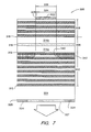
- Figure 7 shows a cross-sectional view of an alternative embodiment of bottom emitting multimode VCSEL structure.
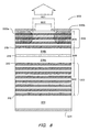
- Figure 8 shows a cross-sectional view of an alternative embodiment of top emitting multimode VCSEL.
- FIG. 3 shows a cross-sectional view of a first embodiment of bottom emitting multimode VCSEL 300.
- the multimode VCSEL 300 includes a first Bragg mirror region 302 grown on a n substrate 304, an active region 306, and a second Bragg mirror region 308 including proton isolation regions 320.
- the VCSEL 300 is grown on an n+ GaAs (gallium arsenide) substrate.
- the GaAs substrate 304 is doped with an n-type dopant, preferably silicon, and has a silicon dopant concentration typically in the range of 5 x 10 17 to 5 x 10 19 atoms/cm 3 .
- the Bragg mirror regions 302, 308 and the active region 306 are formed using techniques well known in the art.
- the first Bragg mirror region 302 is grown on a first surface 312 of the substrate 304 and is typically constructed from alternating quarter-wave layers having different indices of refraction.
- the alternating quarter-wave layers are typically constructed of AlAs and GaAs.
- the interface between the layers may be graded using an AlAs/GaAs/Al 0.3 Ga 0.7 As variable duty cycle short period superlattice to reduce any heterojunction band discontinuities at the GaAs/AlAs interface.
- multimode lasers are designed to provide the maximum power output.
- the maximum power output is typically also defined as the optimal power.
- the textbook Lasers, by A.Siegman, pages 473-479 discusses laser output power.
- mirror reflectivity is increased so that the output power is less than half the optimal power.
- the mirror reflectivity is increased so that the output power is less than 10% of the optimal power.
- FIG. 4 shows a graphical representation of the laser output power versus reflectivity.
- the x axis represents (1-R) where R is the total cavity reflectivity. Thus, the origin (point 402) represents 100% reflectivity.
- the y axis represents the laser output power.
- the point 404 represents the optimal power output of the laser and point 406 on the y axis represents 1 ⁇ 2 the optimal power output of the laser.
- the reflectivity of the multimode laser is designed around point 408. In this embodiment, the reflectivity of the multimode laser is designed so that the output power is less than 1 ⁇ 2 the optimal power.
- the reflectivity of the first and second mirror regions 303, 309 is high, typically greater than 99.5%.
- the first mirror region 303 (the output mirror) has a reflectivity typically around 99.8%.
- the reflectivity of 99.8% for the first mirror region (the output mirror) is true for the bottom emitting structure.
- the first mirror region has a reflectivity typically greater than 99.9% and the second mirror is the output mirror with a reflectivity of greater than 99.5%.
- the first Bragg mirror region 302 is comprised of 21.5 or more pairs of alternating GaAs/AlAs quarter-wave layers having a n-dopant concentration in the range of 10 17 to 10 19 atoms/cm 3 .
- the active region 306 of the VCSEL 300 is formed on a first surface 313 of the active region 306.
- the active region 306 typically includes an n-cladding layer 314a, a quantum well region 316, and a p-cladding layer 314b.
- the cladding layers 314a, 314b are preferably constructed of Al 0.3 Ga 0.7 As doped in the range of 1 to 10 x 10 18 atoms/cm 3 .
- the second Bragg mirror region 308 is formed on the top surface 318 of the active region 306. Similar to the first Bragg mirror 302, the second Bragg mirror 308 is comprised of alternating quarter-wave layers having different indices of refraction, however, the second Bragg mirror 308 is p-doped. The reflectivity of the second Bragg mirror is high, typically around 97% -98%. To achieve this high reflectivity, the second Bragg mirror region 308 includes typically between 15 to 20 pairs of alternating layers of AlAs doped with carbon C or beryllium (Be). The alternating layers have a dopant concentration of 1 x 10 19 atoms/cm 3 and GaAs doped with C or Be.
- the interface between the alternating layers may be graded using an AlAs/GaAs/Al(0.3)Ga(0.7)As variable duty cycle short period superlattice to reduce any heterojunction band discontinuities at the GaAs/AlAs alternating layer interface.
- the mirror reflectivity of the first mirror 303 and second mirrors 309 are designed to have a reflectivity greater than 99.5%.
- the first and second mirror regions 303, 309 may be comprised of a Bragg mirror alone or a Bragg mirror in combination with an electrode mirror.
- the electrode 322 is preferably made of gold, a highly reflective material.
- the reflectivity of the second Bragg mirror 308 is approximately 97%-98%
- the reflectivity of the second mirror region 309 is greater than 99%.
- the reflectivity of the second mirror region 309 is 99.8%.
- Figure 5A shows a graphical representation of RIN versus frequency for different mode/filaments of a multimode laser.
- the multimode of the present invention has similar characteristics except that the vertical cavity surface emitting multimode laser of Figure 5A has higher reflectivity than conventional multimode lasers.
- the reflectivity of both the first mirror region and the second mirror regions should be greater than 99.5%.
- the first relaxation frequency 508 (the lowest relaxation oscillation frequency) shown in Figure 5A is greater than the first relaxation frequency 208 of Figure 2A.
- increasing the mirror reflectivity decreases RIN at the operating frequency. Since the relaxation oscillation frequency is greater than the operating frequency, the multimode laser of Figure 5A and 5B can operate at data rates exceeding gigabits per second with low BER (less than 10 -9 errors/bit). Further, at data rates of one gigabit per second, RIN is less than -130dB/Hz, achieving an acceptable BER.
- the optically lossy regions are proton isolation regions, although other optically lossy regions or alternatively highly resistive regions may be used instead of the optically lossy regions shown in Figures 3 and 5-8 which is induced by ion implantation of hydrogen.
- the proton isolation regions 320 which introduce regions of high resistance, are typically formed in the second Bragg mirror 308.
- An electrode 322 is formed on a first surface of the second Bragg mirror.
- Electrodes 324 are formed on the bottom surface 325 of the substrate 304.
- the aperture of the VCSEL greater than six microns is defined as a multimode laser and a VCSEL having an aperture of less than six microns is defined as a single mode VCSEL, although what is important for a multimode mode laser is the existence of multiple modes/filaments in the cavity.
- the aperture of the laser is defined by the Au mirror 322 in this case.
- the Q for each mode is different, especially near the boundary of the optical lossy regions. Applicant believes by moving the optically lossy regions so that they do not interfere with the outermost modes of the multimode laser, similar Qs for each of the different modes can be achieved. Thus, the lateral dimensions of the optical cavity should be made less than the spacing between the optical lossy regions. When this occurs, similar Qs occur for the multimode laser assuming uniform material parameters.
- the differences in Q between the modes results in spread of the relaxation frequency oscillation of the different modes.
- the embodiment of the multimode laser represented by Figure 5C has high reflectivity to increase the relaxation oscillation frequency, but also has Qs more similar than the Qs shown in Figure 5A.
- the modal curves are bunched together with the originating and termination frequencies 530, 532 and waveform shapes being similar.
- the origination frequencies of the different modes are less than 20 percent different in value.
- the inventors believe that although modal curves having similar Q are preferred, the modal frequency curves do not necessarily have to be bunched together. What is important is that the relaxation oscillation frequency peaks 508 are increased past the operating frequency 540 for a desired RIN at the operating frequency.
- the heretofore described plane through the proton isolation region boundary 326 ends before a plane extending through the corresponding sidewall boundary 328 of the electrode 322.
- the boundary 326 ends two to four microns before the corresponding boundary of the electrode sidewall.
- the proton isolation region boundary 326 typically coincides with or is underneath the electrode 322.
- the width 334 defines the width of the top electrode 322.
- the width 336 defines the proton isolation region diameter, the distance between the two proton isolation regions 320a, 320b.
- the two proton isolation regions 320a, 320b are centered around the central axis of the electrode 322.
- the proton isolation region diameter 336 is larger than the electrode width 334. This is in contrast to conventional single mode and multimode VCSELs where the proton isolation region diameter is either equal to or less than the electrode width.
- Figure 3 shows a cross-sectional view of a first embodiment of bottom emitting multimode VCSEL 300.
- Figure 6 shows a cross-sectional view of an alternative embodiment of bottom emitting multimode VCSEL 300.
- the plane defining the top surface 330 of the proton isolation region 320 coincides with the plane defining the top surface 332 of the second Bragg mirror region 308 upon which an electrode 322 is formed.
- the top surface 332 of the second Bragg mirror region 308 is positioned above the top surface 330 of the proton isolation region 320, where the top surface 332 of the second Bragg mirror region 308 is generally parallel to the top surface 330 of the proton isolation region.
- Figure 7 shows a cross-sectional view of an alternative embodiment of bottom emitting multimode VCSEL structure.
- the optical lossy region are formed using a buried oxygen implant. Oxygen implantation to form current constriction regions is described in U.S. Patent No. 5,266,503.
- the oxygen implant is done in the first Bragg mirror region.
- the boundary 340 of the oxygen implant regions 342 is typically centered around the electrode.
- the distance between the oxygen implant regions 342 is typically greater than the electrode width 334.
- Figure 8 shows a cross-sectional view of an alternative embodiment of top emitting multimode VCSEL. Similar to the embodiments shown in Figures 3, 6 and 7, the lateral distance between the optically lossy regions 801 is greater than the lateral dimensions of the optical cavity, in this case defined approximately by 802. In the embodiment shown in Figure 8, the distance between the sidewalls of the electrode 802 is less than the distance between the proton isolation regions 801. The output mirror reflectivity 308 is greater than 99.5% and the highest reflectivity mirror 302 is greater than 99.9%.
- the multimode VCSEL shown in Figures 3 and 6-8 are not to scale.
- the first and second Bragg mirror regions 304, 308 and the active region 306 have been expanded to provide clarity in the drawings.
- the thickness of the substrate region 304 is approximately 150 ⁇ m as compared to about a 10 ⁇ m combined thicknesses of the Bragg mirror regions 302, 308, and the active regions 306.
- the electrode 322 is approximately 10 ⁇ m in diameter, while electrodes 324 form an opening of approximately 120 - 150 ⁇ m.
- the preferred method of making the multimode laser 300 includes the steps of: forming a first mirror region 302 on a substrate 304, the first mirror region 302 having a reflectivity greater than 99.5%; forming an active region 306 on the first mirror region 302; forming a second mirror region 308 on the surface of the active region 306, the second mirror region 308 having a reflectivity greater than 99.5%, the reflectivity of the first mirror region 302 and second mirror region 308 being designed such that the power output is less than half the maximum power output.
- Optically lossy regions are also typically formed. The distance between the optically lossy regions is greater than the lateral dimensions of the optical cavity of the multimode laser.
- the boundary of the proton isolation region ends before the sidewalls of an electrode boundary of an electrode formed on the surface of the second mirror region.
- the proton isolation region ends two to four microns before the sidewalls of the electrode.
- the a first surface 330 of the proton isolation region coincides with the surface 332 of the second mirror region 308.
- the step of forming the proton isolation region surface to coincide with the surface 332 of the second mirror region 308 preferably includes the steps of: forming a first mask layer on the surface 330 of the second mirror region 308.
- the first mask is an implant mask
- the first material is a dopant comprised of H+ atoms
- the second mirror region is exposed to the first material by ion implantation.
- H+ atoms having a dopant concentration of 10 13 ions/cm 2 to 10 15 ions/cm 2 are implanted.
- an electrode 322 is formed on the surface 332 of the second mirror region.
- Forming the electrode 322 includes the steps of: depositing a conductive layer, typically gold, on the surface of the second mirror region 308; forming a second mask on the surface of the second mirror region 308; removing a portion of the conductive layer to define the electrode 322; and removing the second mask.
- the method of making the bottom emitting VCSEL typically uses two separate masks in order to form proton isolation regions a predetermined distance away (typically two to four microns) from the plane through the electrode sidewalls. This method is used for a top-emitting VCSEL, however, for a bottom-emitting VCSEL a self-aligning technique is used.
- the substrate is thinned to approximately 4 to 6 mils.
- the second contact is an ohmic contact made using techniques well known in the art.
- an anti-reflection layer 327 is typically deposited on the second surface of the substrate.
- the surface on which the top electrode 322 is formed does not coincide with the first surface of the proton isolation regions.
- the structure shown in Figure 6 is done by performing a mesa etch in the second mirror region.
- the proton implant is performed before the mesa etch of the second mirror region, alternative the proton implant may be performed after the mesa etch.
- a proton implant improves multimode laser functionality, alternatively the proton implant step may be eliminated.
- the multimode VCSEL structure shown in Figure 6, preferably includes the steps of: forming a conductive layer, preferably gold (Au), is formed on the surface of the second mirror region; forming a proton isolation mask on the surface of the conductive layer; exposing the second mirror region to a first material; removing a portion of the conductive layer to form a first electrode; removing the proton isolation mask; forming a mesa etch mask; and removing a portion of the second mirror region, the second mirror region being removed to a first height.
- a conductive layer preferably gold (Au)
- Au gold
- a conductive layer typically gold is deposited on the surface of the second mirror region.
- the conductive layer is used for electrode 322 formation.
- a proton isolation mask is formed on the conductive layer so that when exposed to an implant, typically of H+ ions having a dopant concentration in the range of 10 13 ions/cm 2 to 10 15 ions/cm 2 .
- the implant step is followed by an undercutting etch step where the second mirror region is etched approximately a distance of greater than two micrometres. This is followed by an etch of approximately 0.4 micrometres of the second Bragg mirror region. The etch preferably should remove a portion of the second mirror region without totally removing the proton isolation region.
- the multimode laser is bottom emitting, this is not critical.
- the multimode laser may be top-emitting.
- the number of DBR pairs and dopant concentrations for the top-emitting laser may vary.
- different materials may be used and the number of DBR pairs to achieve the desired R (reflectivity).
- the mirror regions may be made of other materials than AlAs and GaAs.
- AlAs and AlGaAs alternating layers may be used.
- different methods may be used for manufacturing the multimode VCSELs shown in Figure 3, and 6-8.
- Further other optically lossy regions than proton isolation regions may be used.
- highly resistive regions such as native oxide may be used instead of optically lossy regions.
Landscapes
- Physics & Mathematics (AREA)
- Optics & Photonics (AREA)
- Chemical & Material Sciences (AREA)
- Engineering & Computer Science (AREA)
- Nanotechnology (AREA)
- Condensed Matter Physics & Semiconductors (AREA)
- General Physics & Mathematics (AREA)
- Electromagnetism (AREA)
- Life Sciences & Earth Sciences (AREA)
- Biophysics (AREA)
- Crystallography & Structural Chemistry (AREA)
- Semiconductor Lasers (AREA)
Claims (7)
- Ein rauscharmer oberflächenemittierender Vertikalresonatorlaser (300), mit folgenden Merkmalen:einer ersten Spiegelregion (302), die ein Reflexionsvermögen von mehr als 99,5% aufweist;einer aktiven Region (306) für eine Laserlichterzeugung bei einer Laserlichtfrequenz, wobei dieselbe zwischen der ersten Spiegelregion (302) und einer zweiten Spiegelregion (308) positioniert ist, die ein Reflexionsvermögen von größer als 99,5% aufweist, wobei die Reflexionsvermögen der ersten Spiegelregion (302) und der zweiten Spiegelregion (308) derart entworfen sind, daß der geometrische Mittelwert der Reflexionsvermögen von beiden Spiegelregionen (302, 308) im Vergleich zu dem entsprechenden geometrischen Mittelwert der Reflexionsvermögen, die für eine maximale Ausgangsleistung bei der Laserlichtfrequenz erforderlich sind, größer ist, und derart, daß die Ausgangsleistung kleiner als die Hälfte der maximalen Ausgangsleistung ist, und daß der Wert des relativen Intensitätsrauschens bei der Laserfrequenz niedriger als derselbe ist, der dem mittleren Reflexionsvermögen bei maximaler Ausgangsleistung entspricht;einer ersten optisch verlustbehafteten Region und einer zweiten optisch verlustbehafteten Region (320; 342), wobei der kürzeste Abstand zwischen der ersten und der zweiten optisch verlustbehafteten Region (336) größer als die Abmessungen des optischen Resonators des Multimodelasers (334) in einer Richtung ist, die quer zu der Lichtemissionsrichtung liegt, und wobei ferner die erste und die zweite optisch verlustbehaftete Region derart positioniert sind, daß dieselben nicht wesentlich die äußersten Moden des oberflächenemittierenden Multimodevertikalresonatorlasers stören.
- Ein Multimodelaser gemäß Anspruch 1, bei dem die zweite Spiegelregion (308) eine Bragg-Spiegelregion und eine Elektrode (322) aufweist, die Reflexionseigenschaften aufweist, und die auf der Oberfläche (332) der zweiten Spiegelregion (308) entgegengesetzt und entfernt von der aktiven Region positioniert ist.
- Ein Multimodelaser gemäß Anspruch 2, bei dem eine Ebene, die parallel zu einer Mittelachse der Elektrode in der Lichtemissionsrichtung ist, und die sich durch den Grenzabschnitt der optisch verlustbehafteten Region (320, 342), der am nächsten zu der Mittelachse ist, erstreckt, vor einer Ebene endet, die sich durch eine entsprechende Seitenwandgrenze der Elektrode (322) erstreckt, die näher zu der Mittelachse ist.
- Ein Multimodelaser gemäß Anspruch 3, bei dem die Ebene, die sich durch den Grenzabschnitt der optisch verlustbehafteten Region (320, 342) erstreckt, etwa 2 bis 4 µm vor der entsprechenden Ebene durch die Seitenwände der Elektrode (322) endet.
- Ein Multimodelaser gemäß Anspruch 3 oder 4, bei dem die Ebene, die die obere Oberfläche der optisch verlustbehafteten Region (330) bildet, mit der Ebene zusammenfällt, die die obere Oberfläche (332) der zweiten Bragg-Spiegelregion (308) bildet, auf der die Elektrode (322) gebildet ist.
- Ein Multimodelaser gemäß einem beliebigen der Ansprüche 3 bis 5, bei dem der Abstand zwischen den optisch verlustbehafteten Regionen (320, 342) größer als die Breite der Elektrode ist, die auf der Oberfläche der zweiten Spiegelregion (308) gebildet ist.
- Ein Verfahren zum Herstellen eines rauscharmen oberflächenemittierenden Multimodevertikalresonatorlasers, mit folgenden Schritten:Bilden einer ersten Spiegelregion (302), die ein Reflexionsvermögen von mehr als 99,5% aufweist;Bilden einer aktiven Region (306) für eine Laserlichterzeugung bei einer Laserlichtfrequenz auf einer ersten Oberfläche der ersten Spiegelregion (302);Bilden einer zweiten Spiegelregion (308), die ein Reflexionsvermögen von mehr als 99,5% aufweist, auf der Oberfläche der aktiven Region (306), derart, daß die aktive Region (306) zwischen der ersten (302) und der zweiten (308) Spiegelregion positioniert ist, wobei die Reflexionsvermögen der ersten (302) und der zweiten (308) Spiegelregion derart entworfen sind, daß der geometrische Mittelwert der Reflexionsvermögen derselben im Vergleich zu dem entsprechenden geometrischen Mittelwert der Reflexionsvermögen, die für eine maximale Ausgangsleistung bei der Laserlichtfrequenz erforderlich sind, größer ist, und derart, daß die Ausgangsleistung kleiner als die Hälfte der maximalen Ausgangsleistung ist, und daß der Wert des relativen Intensitätsrauschens bei der Laserlichtfrequenz kleiner als derselbe ist, der dem mittleren Reflexionsvermögen bei maximaler Ausgangsleistung entspricht; undBilden einer ersten und einer zweiten optisch verlustbehafteten Region (320; 342), wobei der kürzeste Abstand zwischen denselben größer als die Abmessung des optischen Resonators des Multimodelasers in einer Richtung ist, die quer zu der Lichtemissionsrichtung liegt, und wobei die erste und die zweite optisch verlustbehaftete Region (320; 342) derart positioniert sind, daß dieselben die äußersten Moden des oberflächenemittierenden Multimodevertikalresonatorlasers nicht wesentlich stören.
Applications Claiming Priority (2)
| Application Number | Priority Date | Filing Date | Title |
|---|---|---|---|
| US447657 | 1995-05-23 | ||
| US08/447,657 US5659568A (en) | 1995-05-23 | 1995-05-23 | Low noise surface emitting laser for multimode optical link applications |
Publications (3)
| Publication Number | Publication Date |
|---|---|
| EP0744799A2 EP0744799A2 (de) | 1996-11-27 |
| EP0744799A3 EP0744799A3 (de) | 1997-09-17 |
| EP0744799B1 true EP0744799B1 (de) | 1999-11-24 |
Family
ID=23777222
Family Applications (1)
| Application Number | Title | Priority Date | Filing Date |
|---|---|---|---|
| EP96303551A Expired - Lifetime EP0744799B1 (de) | 1995-05-23 | 1996-05-20 | Laser |
Country Status (4)
| Country | Link |
|---|---|
| US (1) | US5659568A (de) |
| EP (1) | EP0744799B1 (de) |
| JP (1) | JP3720454B2 (de) |
| DE (1) | DE69605245T2 (de) |
Families Citing this family (25)
| Publication number | Priority date | Publication date | Assignee | Title |
|---|---|---|---|---|
| US5724376A (en) * | 1995-11-30 | 1998-03-03 | Hewlett-Packard Company | Transparent substrate vertical cavity surface emitting lasers fabricated by semiconductor wafer bonding |
| US5808770A (en) * | 1995-12-29 | 1998-09-15 | Lucent Technologies, Inc. | Method and apparatus for using on-off-keying using laser relaxation oscillation |
| US5867516A (en) * | 1996-03-12 | 1999-02-02 | Hewlett-Packard Company | Vertical cavity surface emitting laser with reduced turn-on jitter and increased single-mode output |
| US5774487A (en) * | 1996-10-16 | 1998-06-30 | Honeywell Inc. | Filamented multi-wavelength vertical-cavity surface emitting laser |
| US5903588A (en) * | 1997-03-06 | 1999-05-11 | Honeywell Inc. | Laser with a selectively changed current confining layer |
| AU747260B2 (en) | 1997-07-25 | 2002-05-09 | Nichia Chemical Industries, Ltd. | Nitride semiconductor device |
| WO1999021252A1 (en) * | 1997-10-23 | 1999-04-29 | Honeywell Inc. | Filamented multi-wavelength vertical-cavity surface emitting laser |
| US6556329B1 (en) | 1998-05-21 | 2003-04-29 | Enterasys Networks, Inc. | Method and system for preventing low order optical transmission modes in multimode optical fiber computer network using annulus laser |
| US6154589A (en) | 1998-05-21 | 2000-11-28 | Cabletron Systems, Inc. | Method and system for removal of low order optical transmission modes in multimode optical fiber computer network to improve modal bandwidth |
| JP3770014B2 (ja) | 1999-02-09 | 2006-04-26 | 日亜化学工業株式会社 | 窒化物半導体素子 |
| ATE200944T1 (de) * | 1999-02-11 | 2001-05-15 | Avalon Photonics Ltd | Halbleiterlaser und herstellungsverfahren |
| ATE452445T1 (de) | 1999-03-04 | 2010-01-15 | Nichia Corp | Nitridhalbleiterlaserelement |
| EP1146615A4 (de) * | 1999-09-22 | 2005-10-19 | Mitsubishi Chem Corp | Leuchtendes element und modul mit leuchtenden elementen |
| WO2002101894A1 (en) * | 2001-05-31 | 2002-12-19 | Nichia Corporation | Semiconductor laser element |
| KR20030045252A (ko) * | 2001-12-01 | 2003-06-11 | 주식회사 나노트론 | 장파장 면발광 반도체 레이저 다이오드 |
| KR100440254B1 (ko) * | 2002-06-07 | 2004-07-15 | 한국전자통신연구원 | 안티가이드형 표면방출 레이저 및 제조 방법 |
| DE10261238A1 (de) * | 2002-12-20 | 2004-07-15 | Forschungszentrum Jülich GmbH | Schichtenfolge |
| JP2004288674A (ja) * | 2003-03-19 | 2004-10-14 | Fuji Xerox Co Ltd | 面発光型半導体レーザおよびそれを用いた光通信システム |
| US7218660B2 (en) * | 2003-10-27 | 2007-05-15 | Avago Technologies Fiber Ip (Singapore) Pte. Ltd. | Single-mode vertical cavity surface emitting lasers and methods of making the same |
| US20050191059A1 (en) * | 2004-01-12 | 2005-09-01 | Clariphy | Use of low-speed components in high-speed optical fiber transceivers |
| JP2009529243A (ja) * | 2006-03-07 | 2009-08-13 | メアリー ケイ ブレナー | 赤色発光レーザ |
| JP2006237648A (ja) * | 2006-06-07 | 2006-09-07 | Fuji Xerox Co Ltd | 面発光型半導体レーザ |
| TWI362769B (en) | 2008-05-09 | 2012-04-21 | Univ Nat Chiao Tung | Light emitting device and fabrication method therefor |
| US9281661B2 (en) * | 2014-07-02 | 2016-03-08 | Avago Technologies General Ip (Singapore) Pte. Ltd. | Integrated optoelectronic device comprising a Mach-Zehnder modulator and a vertical cavity surface emitting laser (VCSEL) |
| US12019200B2 (en) * | 2019-03-12 | 2024-06-25 | Saudi Arabian Oil Company | Downhole monitoring using few-mode optical fiber based distributed acoustic sensing |
Family Cites Families (6)
| Publication number | Priority date | Publication date | Assignee | Title |
|---|---|---|---|---|
| US5063569A (en) * | 1990-12-19 | 1991-11-05 | At&T Bell Laboratories | Vertical-cavity surface-emitting laser with non-epitaxial multilayered dielectric reflectors located on both surfaces |
| US5206872A (en) * | 1991-11-01 | 1993-04-27 | At&T Bell Laboratories | Surface emitting laser |
| US5256596A (en) * | 1992-03-26 | 1993-10-26 | Motorola, Inc. | Top emitting VCSEL with implant |
| US5274655A (en) * | 1992-03-26 | 1993-12-28 | Motorola, Inc. | Temperature insensitive vertical cavity surface emitting laser |
| US5328854A (en) * | 1993-03-31 | 1994-07-12 | At&T Bell Laboratories | Fabrication of electronic devices with an internal window |
| US5359447A (en) * | 1993-06-25 | 1994-10-25 | Hewlett-Packard Company | Optical communication with vertical-cavity surface-emitting laser operating in multiple transverse modes |
-
1995
- 1995-05-23 US US08/447,657 patent/US5659568A/en not_active Expired - Lifetime
-
1996
- 1996-05-20 DE DE69605245T patent/DE69605245T2/de not_active Expired - Lifetime
- 1996-05-20 EP EP96303551A patent/EP0744799B1/de not_active Expired - Lifetime
- 1996-05-23 JP JP12871896A patent/JP3720454B2/ja not_active Expired - Lifetime
Also Published As
| Publication number | Publication date |
|---|---|
| JP3720454B2 (ja) | 2005-11-30 |
| DE69605245D1 (de) | 1999-12-30 |
| DE69605245T2 (de) | 2001-10-18 |
| US5659568A (en) | 1997-08-19 |
| JPH09102648A (ja) | 1997-04-15 |
| EP0744799A3 (de) | 1997-09-17 |
| EP0744799A2 (de) | 1996-11-27 |
Similar Documents
| Publication | Publication Date | Title |
|---|---|---|
| US5659568A (en) | Low noise surface emitting laser for multimode optical link applications | |
| US6931042B2 (en) | Long wavelength vertical cavity surface emitting laser | |
| KR100229052B1 (ko) | 전류애퍼쳐가형성되어있는수직캐비티레이저 | |
| US6898215B2 (en) | Long wavelength vertical cavity surface emitting laser | |
| US8254424B2 (en) | Semiconductor having enhanced carbon doping | |
| US6577658B1 (en) | Method and apparatus for planar index guided vertical cavity surface emitting lasers | |
| US5903590A (en) | Vertical-cavity surface-emitting laser device | |
| EP1073171B1 (de) | Oberflächenemittierender Laser mit vertikalem Resonator und lateraler Ladungsträgerinjektion | |
| US7501294B1 (en) | VCSEL for high speed lower power optical link | |
| US8193019B2 (en) | Vertical cavity surface emitting laser having multiple top-side contacts | |
| GB2370689A (en) | Vertical cavity surface emitting laser with reduced parasitic capacitance | |
| US20190089127A1 (en) | Vcsel with elliptical aperture having reduced rin | |
| WO2001093387A2 (en) | Long wavelength vertical cavity surface emitting laser | |
| US6011811A (en) | Buried heterostructure with aluminum-free active layer and method of making same | |
| US7408967B2 (en) | Method of fabricating single mode VCSEL for optical mouse | |
| US6882673B1 (en) | Mirror structure for reducing the effect of feedback on a VCSEL | |
| US6906353B1 (en) | High speed implanted VCSEL | |
| US7154927B2 (en) | Surface emitting semiconductor laser and communication system using the same | |
| US7095771B2 (en) | Implant damaged oxide insulating region in vertical cavity surface emitting laser | |
| JP2002111125A (ja) | 分布帰還型半導体レーザ |
Legal Events
| Date | Code | Title | Description |
|---|---|---|---|
| PUAI | Public reference made under article 153(3) epc to a published international application that has entered the european phase |
Free format text: ORIGINAL CODE: 0009012 |
|
| AK | Designated contracting states |
Kind code of ref document: A2 Designated state(s): DE FR GB |
|
| PUAL | Search report despatched |
Free format text: ORIGINAL CODE: 0009013 |
|
| AK | Designated contracting states |
Kind code of ref document: A3 Designated state(s): DE FR GB |
|
| 17P | Request for examination filed |
Effective date: 19980302 |
|
| 17Q | First examination report despatched |
Effective date: 19980819 |
|
| GRAG | Despatch of communication of intention to grant |
Free format text: ORIGINAL CODE: EPIDOS AGRA |
|
| GRAG | Despatch of communication of intention to grant |
Free format text: ORIGINAL CODE: EPIDOS AGRA |
|
| GRAH | Despatch of communication of intention to grant a patent |
Free format text: ORIGINAL CODE: EPIDOS IGRA |
|
| GRAH | Despatch of communication of intention to grant a patent |
Free format text: ORIGINAL CODE: EPIDOS IGRA |
|
| GRAA | (expected) grant |
Free format text: ORIGINAL CODE: 0009210 |
|
| AK | Designated contracting states |
Kind code of ref document: B1 Designated state(s): DE FR GB |
|
| REF | Corresponds to: |
Ref document number: 69605245 Country of ref document: DE Date of ref document: 19991230 |
|
| ET | Fr: translation filed | ||
| PLBE | No opposition filed within time limit |
Free format text: ORIGINAL CODE: 0009261 |
|
| STAA | Information on the status of an ep patent application or granted ep patent |
Free format text: STATUS: NO OPPOSITION FILED WITHIN TIME LIMIT |
|
| 26N | No opposition filed | ||
| REG | Reference to a national code |
Ref country code: GB Ref legal event code: 732E |
|
| REG | Reference to a national code |
Ref country code: FR Ref legal event code: TP |
|
| REG | Reference to a national code |
Ref country code: GB Ref legal event code: IF02 |
|
| PGFP | Annual fee paid to national office [announced via postgrant information from national office to epo] |
Ref country code: FR Payment date: 20060517 Year of fee payment: 11 |
|
| REG | Reference to a national code |
Ref country code: GB Ref legal event code: 732E |
|
| REG | Reference to a national code |
Ref country code: GB Ref legal event code: 732E |
|
| REG | Reference to a national code |
Ref country code: FR Ref legal event code: ST Effective date: 20080131 |
|
| PG25 | Lapsed in a contracting state [announced via postgrant information from national office to epo] |
Ref country code: FR Free format text: LAPSE BECAUSE OF NON-PAYMENT OF DUE FEES Effective date: 20070531 |
|
| REG | Reference to a national code |
Ref country code: DE Ref legal event code: R082 Ref document number: 69605245 Country of ref document: DE Representative=s name: DILG HAEUSLER SCHINDELMANN PATENTANWALTSGESELL, DE |
|
| REG | Reference to a national code |
Ref country code: GB Ref legal event code: 732E Free format text: REGISTERED BETWEEN 20130725 AND 20130731 |
|
| REG | Reference to a national code |
Ref country code: DE Ref legal event code: R082 Ref document number: 69605245 Country of ref document: DE Representative=s name: DILG HAEUSLER SCHINDELMANN PATENTANWALTSGESELL, DE Effective date: 20130628 Ref country code: DE Ref legal event code: R081 Ref document number: 69605245 Country of ref document: DE Owner name: AVAGO TECHNOLOGIES GENERAL IP (SINGAPORE) PTE., SG Free format text: FORMER OWNER: AVAGO TECHNOLOGIES FIBER IP (SINGAPORE) PTE. LTD., SINGAPORE, SG Effective date: 20130628 |
|
| PGFP | Annual fee paid to national office [announced via postgrant information from national office to epo] |
Ref country code: DE Payment date: 20150422 Year of fee payment: 20 Ref country code: GB Payment date: 20150424 Year of fee payment: 20 |
|
| REG | Reference to a national code |
Ref country code: DE Ref legal event code: R071 Ref document number: 69605245 Country of ref document: DE |
|
| REG | Reference to a national code |
Ref country code: GB Ref legal event code: PE20 Expiry date: 20160519 |
|
| PG25 | Lapsed in a contracting state [announced via postgrant information from national office to epo] |
Ref country code: GB Free format text: LAPSE BECAUSE OF EXPIRATION OF PROTECTION Effective date: 20160519 |