EP0742904B1 - Method of making a micromechanical silicon-on-glass tuning fork gyroscope - Google Patents
Method of making a micromechanical silicon-on-glass tuning fork gyroscope Download PDFInfo
- Publication number
- EP0742904B1 EP0742904B1 EP95909430A EP95909430A EP0742904B1 EP 0742904 B1 EP0742904 B1 EP 0742904B1 EP 95909430 A EP95909430 A EP 95909430A EP 95909430 A EP95909430 A EP 95909430A EP 0742904 B1 EP0742904 B1 EP 0742904B1
- Authority
- EP
- European Patent Office
- Prior art keywords
- substrate
- metallic layer
- silicon substrate
- etching
- silicon
- Prior art date
- Legal status (The legal status is an assumption and is not a legal conclusion. Google has not performed a legal analysis and makes no representation as to the accuracy of the status listed.)
- Expired - Lifetime
Links
- 239000011521 glass Substances 0.000 title claims description 49
- 238000004519 manufacturing process Methods 0.000 title description 11
- 239000000758 substrate Substances 0.000 claims description 86
- XUIMIQQOPSSXEZ-UHFFFAOYSA-N Silicon Chemical compound [Si] XUIMIQQOPSSXEZ-UHFFFAOYSA-N 0.000 claims description 71
- 229910052710 silicon Inorganic materials 0.000 claims description 66
- 239000010703 silicon Substances 0.000 claims description 66
- 238000000034 method Methods 0.000 claims description 49
- 229910052751 metal Inorganic materials 0.000 claims description 29
- 239000002184 metal Substances 0.000 claims description 29
- BASFCYQUMIYNBI-UHFFFAOYSA-N platinum Chemical compound [Pt] BASFCYQUMIYNBI-UHFFFAOYSA-N 0.000 claims description 28
- 238000005530 etching Methods 0.000 claims description 23
- PCHJSUWPFVWCPO-UHFFFAOYSA-N gold Chemical compound [Au] PCHJSUWPFVWCPO-UHFFFAOYSA-N 0.000 claims description 19
- 229910052737 gold Inorganic materials 0.000 claims description 19
- 239000010931 gold Substances 0.000 claims description 19
- 229910052697 platinum Inorganic materials 0.000 claims description 14
- KWYUFKZDYYNOTN-UHFFFAOYSA-M Potassium hydroxide Chemical compound [OH-].[K+] KWYUFKZDYYNOTN-UHFFFAOYSA-M 0.000 claims description 8
- ZOXJGFHDIHLPTG-UHFFFAOYSA-N Boron Chemical compound [B] ZOXJGFHDIHLPTG-UHFFFAOYSA-N 0.000 claims description 6
- 229910052796 boron Inorganic materials 0.000 claims description 6
- 238000000151 deposition Methods 0.000 claims description 6
- 230000000873 masking effect Effects 0.000 claims description 6
- RTAQQCXQSZGOHL-UHFFFAOYSA-N Titanium Chemical compound [Ti] RTAQQCXQSZGOHL-UHFFFAOYSA-N 0.000 claims description 5
- 230000035945 sensitivity Effects 0.000 claims description 5
- 239000010936 titanium Substances 0.000 claims description 5
- 229910052719 titanium Inorganic materials 0.000 claims description 5
- KRHYYFGTRYWZRS-UHFFFAOYSA-N Fluorane Chemical compound F KRHYYFGTRYWZRS-UHFFFAOYSA-N 0.000 claims description 4
- 239000002019 doping agent Substances 0.000 claims description 4
- RJCQBQGAPKAMLL-UHFFFAOYSA-N bromotrifluoromethane Chemical compound FC(F)(F)Br RJCQBQGAPKAMLL-UHFFFAOYSA-N 0.000 claims description 3
- XLYOFNOQVPJJNP-UHFFFAOYSA-N water Substances O XLYOFNOQVPJJNP-UHFFFAOYSA-N 0.000 claims description 2
- 230000008021 deposition Effects 0.000 claims 2
- 235000012431 wafers Nutrition 0.000 description 12
- 238000009792 diffusion process Methods 0.000 description 7
- 230000008569 process Effects 0.000 description 7
- 230000000712 assembly Effects 0.000 description 6
- 238000000429 assembly Methods 0.000 description 6
- CPELXLSAUQHCOX-UHFFFAOYSA-N Hydrogen bromide Chemical compound Br CPELXLSAUQHCOX-UHFFFAOYSA-N 0.000 description 4
- 230000009467 reduction Effects 0.000 description 4
- 230000009286 beneficial effect Effects 0.000 description 3
- 230000006835 compression Effects 0.000 description 3
- 238000007906 compression Methods 0.000 description 3
- 150000002739 metals Chemical class 0.000 description 3
- KZBUYRJDOAKODT-UHFFFAOYSA-N Chlorine Chemical compound ClCl KZBUYRJDOAKODT-UHFFFAOYSA-N 0.000 description 2
- 230000008859 change Effects 0.000 description 2
- 239000004020 conductor Substances 0.000 description 2
- FHUGMWWUMCDXBC-UHFFFAOYSA-N gold platinum titanium Chemical compound [Ti][Pt][Au] FHUGMWWUMCDXBC-UHFFFAOYSA-N 0.000 description 2
- 229910000042 hydrogen bromide Inorganic materials 0.000 description 2
- 230000003071 parasitic effect Effects 0.000 description 2
- 239000000126 substance Substances 0.000 description 2
- TXEYQDLBPFQVAA-UHFFFAOYSA-N tetrafluoromethane Chemical compound FC(F)(F)F TXEYQDLBPFQVAA-UHFFFAOYSA-N 0.000 description 2
- FAQYAMRNWDIXMY-UHFFFAOYSA-N trichloroborane Chemical compound ClB(Cl)Cl FAQYAMRNWDIXMY-UHFFFAOYSA-N 0.000 description 2
- ZCYVEMRRCGMTRW-UHFFFAOYSA-N 7553-56-2 Chemical group [I] ZCYVEMRRCGMTRW-UHFFFAOYSA-N 0.000 description 1
- 229910015844 BCl3 Inorganic materials 0.000 description 1
- ZOKXTWBITQBERF-UHFFFAOYSA-N Molybdenum Chemical compound [Mo] ZOKXTWBITQBERF-UHFFFAOYSA-N 0.000 description 1
- ADNDKZZPECQWEJ-UHFFFAOYSA-N acetic acid;nitric acid;hydrofluoride Chemical compound F.CC(O)=O.O[N+]([O-])=O ADNDKZZPECQWEJ-UHFFFAOYSA-N 0.000 description 1
- 239000002318 adhesion promoter Substances 0.000 description 1
- 239000000853 adhesive Substances 0.000 description 1
- 230000001070 adhesive effect Effects 0.000 description 1
- 229910045601 alloy Inorganic materials 0.000 description 1
- 239000000956 alloy Substances 0.000 description 1
- QVGXLLKOCUKJST-UHFFFAOYSA-N atomic oxygen Chemical compound [O] QVGXLLKOCUKJST-UHFFFAOYSA-N 0.000 description 1
- 238000005452 bending Methods 0.000 description 1
- 230000015572 biosynthetic process Effects 0.000 description 1
- 238000006243 chemical reaction Methods 0.000 description 1
- 239000000460 chlorine Substances 0.000 description 1
- 229910052801 chlorine Inorganic materials 0.000 description 1
- 230000000694 effects Effects 0.000 description 1
- 239000007772 electrode material Substances 0.000 description 1
- 239000000835 fiber Substances 0.000 description 1
- JUWSSMXCCAMYGX-UHFFFAOYSA-N gold platinum Chemical compound [Pt].[Au] JUWSSMXCCAMYGX-UHFFFAOYSA-N 0.000 description 1
- ZNKMCMOJCDFGFT-UHFFFAOYSA-N gold titanium Chemical compound [Ti].[Au] ZNKMCMOJCDFGFT-UHFFFAOYSA-N 0.000 description 1
- -1 hydraline Chemical compound 0.000 description 1
- 230000003116 impacting effect Effects 0.000 description 1
- 229910052740 iodine Inorganic materials 0.000 description 1
- 239000011630 iodine Substances 0.000 description 1
- 150000002500 ions Chemical class 0.000 description 1
- 229910052741 iridium Inorganic materials 0.000 description 1
- GKOZUEZYRPOHIO-UHFFFAOYSA-N iridium atom Chemical compound [Ir] GKOZUEZYRPOHIO-UHFFFAOYSA-N 0.000 description 1
- 239000000463 material Substances 0.000 description 1
- 239000012528 membrane Substances 0.000 description 1
- 238000001465 metallisation Methods 0.000 description 1
- 239000000203 mixture Substances 0.000 description 1
- 229910052750 molybdenum Inorganic materials 0.000 description 1
- 239000011733 molybdenum Substances 0.000 description 1
- 239000001301 oxygen Substances 0.000 description 1
- 229910052760 oxygen Inorganic materials 0.000 description 1
- 238000001020 plasma etching Methods 0.000 description 1
- 229910021420 polycrystalline silicon Inorganic materials 0.000 description 1
- 229920005591 polysilicon Polymers 0.000 description 1
- 239000010453 quartz Substances 0.000 description 1
- 230000035939 shock Effects 0.000 description 1
- 229910021332 silicide Inorganic materials 0.000 description 1
- FVBUAEGBCNSCDD-UHFFFAOYSA-N silicide(4-) Chemical compound [Si-4] FVBUAEGBCNSCDD-UHFFFAOYSA-N 0.000 description 1
- VYPSYNLAJGMNEJ-UHFFFAOYSA-N silicon dioxide Inorganic materials O=[Si]=O VYPSYNLAJGMNEJ-UHFFFAOYSA-N 0.000 description 1
- 239000007779 soft material Substances 0.000 description 1
- 239000007787 solid Substances 0.000 description 1
- 229910001258 titanium gold Inorganic materials 0.000 description 1
- 229910021341 titanium silicide Inorganic materials 0.000 description 1
- MAKDTFFYCIMFQP-UHFFFAOYSA-N titanium tungsten Chemical compound [Ti].[W] MAKDTFFYCIMFQP-UHFFFAOYSA-N 0.000 description 1
- WFKWXMTUELFFGS-UHFFFAOYSA-N tungsten Chemical compound [W] WFKWXMTUELFFGS-UHFFFAOYSA-N 0.000 description 1
- 229910052721 tungsten Inorganic materials 0.000 description 1
- 239000010937 tungsten Substances 0.000 description 1
- WQJQOUPTWCFRMM-UHFFFAOYSA-N tungsten disilicide Chemical compound [Si]#[W]#[Si] WQJQOUPTWCFRMM-UHFFFAOYSA-N 0.000 description 1
- 229910021342 tungsten silicide Inorganic materials 0.000 description 1
Images


Classifications
-
- G—PHYSICS
- G01—MEASURING; TESTING
- G01C—MEASURING DISTANCES, LEVELS OR BEARINGS; SURVEYING; NAVIGATION; GYROSCOPIC INSTRUMENTS; PHOTOGRAMMETRY OR VIDEOGRAMMETRY
- G01C19/00—Gyroscopes; Turn-sensitive devices using vibrating masses; Turn-sensitive devices without moving masses; Measuring angular rate using gyroscopic effects
- G01C19/56—Turn-sensitive devices using vibrating masses, e.g. vibratory angular rate sensors based on Coriolis forces
- G01C19/5719—Turn-sensitive devices using vibrating masses, e.g. vibratory angular rate sensors based on Coriolis forces using planar vibrating masses driven in a translation vibration along an axis
-
- Y—GENERAL TAGGING OF NEW TECHNOLOGICAL DEVELOPMENTS; GENERAL TAGGING OF CROSS-SECTIONAL TECHNOLOGIES SPANNING OVER SEVERAL SECTIONS OF THE IPC; TECHNICAL SUBJECTS COVERED BY FORMER USPC CROSS-REFERENCE ART COLLECTIONS [XRACs] AND DIGESTS
- Y10—TECHNICAL SUBJECTS COVERED BY FORMER USPC
- Y10S—TECHNICAL SUBJECTS COVERED BY FORMER USPC CROSS-REFERENCE ART COLLECTIONS [XRACs] AND DIGESTS
- Y10S438/00—Semiconductor device manufacturing: process
- Y10S438/914—Doping
- Y10S438/924—To facilitate selective etching
Definitions
- This invention relates in general to a method of making a micromechanical device, and in particular to a method of making a micromechanical silicon-on-glass tuning fork gyroscope.
- gyroscope There are many methods of performing the functions of a gyroscope: rotating disc, rotating sphere, quartz tuning fork, fiber optic laser, hemispherical resonance, etc.
- micromechanical gyroscope implementations such as gimballed gyroscopes, and polysilicon and metal tuning fork gyroscopes.
- the "bulk” or non-micromechanical gyroscopes are much larger, heavier, and expensive. Previous micromechanical gyroscopes have low sensitivity, are difficult to fabricate due to multiple masking and processing steps, and have problems with movable masses coming into contact with electrode material and sticking.
- Sticking occurs when a resonating mass comes into contact with an underlying metal electrode, typically gold, and fails to spring free, ultimately ending in device failure.
- the magnitude of drive forces and pressures that can be applied to a gyroscope prone to sticking is necessarily limited by this phenomenon.
- a method for fabricating a micromechanical tuning fork gyroscope which includes single sided processing of a silicon substrates and a glass substrate, anodic bonding of the resultant substrate structures, and a final etch step to free the tuning fork elements.
- the method requires fewer and simpler processing steps, thus resulting in a lower cost and easier to fabricate micromechanical gyroscope.
- a comb drive micromechanical tuning fork gyroscope has a first surface of a glass substrate over which is suspended a silicon rotatable assembly comprising first and second vibrating assemblies extending from one or more anchors. Disposed at either end of the respective vibrating assemblies are drive and driven finger electrodes formed by plural respective interleaved fingers for imparting vibrational motion to the tuning fork vibrating elements.
- the finger electrodes greatly increase the area and capacitance as well as the capacitance change with motion of the device so as to substantially enhance system sensitivity.
- the method of fabricating such a gyroscope takes place on a first surface each of a silicon substrate and a glass substrate.
- a silicon substrate With regard to the silicon substrate, one or more recesses are formed using potassium hydroxide (KOH).
- KOH potassium hydroxide
- a single subsequent boron diffusion defines the thickness of the silicon gyroscope structure.
- the features of the structure are defined by using a reactive ion etch (RIE) beyond the boron etch stop layer in selected locations.
- RIE reactive ion etch
- the glass substrate processing involves a first step of selectively recessing the first surface of the glass. Next, a multi-metal system such as titanium-platinum-gold is deposited on the recessed first surface, then selectively lifted off, leaving a planar glass surface with metal deposits only slightly extending beyond the surface.
- a multi-metal system such as titanium-platinum-gold
- one substrate is inverted over the first surface of the other, the two are aligned, and are then anodically bonded.
- Lead transfer to the silicon is achieved through contiguous gold deposits; due to the high temperature at which the binding process occurs, the silicon and gold sinter, thus forming a chemical bond.
- the low profile, recessed metal deposits as described in said publication may provide sufficient reduction in the potential for portions of the silicon gyroscope structure to impact a portion of the multi-metal systems, such impact would likely occur in gyroscopes subject to extreme angular rates and/or physical shocks. Sticking between the silicon and the uppermost gold layer would then result, partially due to gold being a soft material. By removing the gold in an embodiment of the present invention, the exposed surface of the multi-metal system is the hard platinum layer.
- the step of removing the gold from metal deposits subject to silicon impact increases the resistance to sticking.
- a further step can be taken to significantly decrease the likelihood of this device failure mode.
- the platinum layer can be patterned to form an array of stand-offs or posts which reduce the contact area where the masses impact. Since the sticking tendency is a function of surface area in contact, sticking is necessarily reduced by the formation of these platinum stand-offs.
- the tuning fork gyroscope embodiment thus formed provides reduced discrete processing steps with a resultant reduction in production cost and fabrication time, and enhanced resistance to adhesion between the silicon structure, the glass substrate and the metallic electrodes disposed therebetween.
- Another beneficial result of the use of the method disclosed herein includes reduced parasitic capacitance from the use of a glass substrate.
- the present invention contemplates a micromechanical tuning fork gyroscope 10 fabricated by a dissolved silicon wafer process whereby electrostatic bonding forms a hermetic seal between an etched glass substrate 12, metal electrodes deposited thereon, and a silicon comb drive tuning fork gyroscope 14.
- the dissolved silicon wafer process involves single sided processing of a silicon substrate, including the steps of etching recesses, diffusing an etch resistant dopant into the silicon substrate, and releasing various components of the silicon gyroscope by etching through the diffusion layer in desired locations.
- the glass substrate also undergoes single sided processing, including the steps of etching recesses, depositing a multi-metal system in the recesses, and selectively etching portions of the multi-metal system.
- One substrate is inverted over the other and aligned before anodic bonding of the two substrates is performed.
- a comb drive gyroscope 14 fabricated according to the present invention is illustrated.
- the gyroscope thus formed employs drive 16 and driven finger electrodes 18 formed by plural respective interleaved fingers 24 for imparting vibrational motion to the tuning fork vibrating elements 20.
- the finger electrodes greatly increase the area and capacitance as well as the capacitance change with motion of the device so as to substantially enhance system sensitivity.
- such an electrode structure is compatible with the dissolved silicon wafer process disclosed herein.
- the tuning fork gyroscope 14 thus provides reduced parasitic capacitance resulting from the use of a glass substrate, reduced discrete processing steps with a resultant reduction in production cost and fabrication time, and enhanced resistance to adhesion between the silicon structure, the glass substrate and the metallic electrodes disposed therebetween.
- a first surface of a glass substrate has suspended thereover a silicon rotatable assembly 30 comprising first and second vibrating assemblies 20 which extend from one or more anchors 32.
- the vibrating assemblies 20 are comprised of opposing comb structures made up of driven electrode fingers 24 extending therefrom.
- Disposed on the first surface of the glass substrate are cooperating drive electrode fingers 16 for alternating alignment with the driven finger electrodes 18.
- Torque 36, or rebalance, and sense electrodes 38 are disposed on the glass substrate beneath a portion of the vibrating assemblies and/or support structures extending between the vibrating assemblies and the anchors. Also disposed on the glass substrate are metallic conductive leads 40 interconnecting transducers with the electrodes 36, 38 and left 44, right 46, and center drive motors 48. These transducers include left 50 and right torque transducers 52, left 54 and right sense transducers 56, and motor transducer 58.
- the method of fabricating a gyroscope 14 as depicted in Fig. 1 begins with reactive ion etching (RIE) and boron diffusion of silicon to define the suspended gyroscope structure.
- RIE reactive ion etching
- processing starts with a p-type silicon wafer 100 of moderate doping (eg . >1 ⁇ -cm).
- Recesses 102 etched into the silicon using potassium hydroxide (KOH) will eventually define the gap spacing of conducting elements which comprise the electrodes.
- Recesses may also be formed using RIE or plasma techniques.
- a high temperature (eg . 1150-1175°C) boron (p++) diffusion 104 across the surface of the Si substrate follows.
- the diffusion depth which may be in the range of 5 to 10 ⁇ m, defines the thickness of the resulting gyroscope structure.
- the outline of the features of the structure is defined by using RIE to etch past the p++ diffused etch stop layer 104, thus releasing and uniquely defining individual elements of the structure as shown in Fig. 2C.
- a CF 3 Br (trifluorobromomethane) chemistry is used for etching in a parallel plate reactor, thus resulting in straight sidewalls 106 and high aspect ratios.
- BCl 3 /Cl 2 boron tri-chloride/chlorine
- HBr hydrogen bromide
- CF 4 carbon tetrafluoride
- O 2 (oxygen) chemical mixtures can also be used.
- a glass wafer 12 such as a #7740 Corning glass wafer, is selectively etched to form low profile metal deposition sites 200. Hydrofluoric acid or plasma (e.g. RIE) may be used as the glass etchant.
- a multi-metal system 202 is deposited in the etched recesses.
- One embodiment of the present invention employs a titanium-platinum-gold (Ti-Pt-Au) combination for electrode and conductor structures. Titanium 210 is deposited in the glass wafer 12 recess 200 first, for example to a thickness of 0.04 ⁇ m (400 ⁇ ), due to its excellent adhesion to glass.
- platinum 212 is deposited, for example to a depth of 0.07 ⁇ m (700 ⁇ ), on the titanium 210.
- a layer of gold 214 is deposited on the platinum 212.
- the gold 214 makes a superior contact point for wire bonding.
- Employing these exemplary thicknesses produces a planar structure with metal protruding only 0.05 ⁇ m (500 ⁇ ) above the surface of the glass 12.
- the three metals do not alloy with each other, thus enabling electrostatic bonding taking place at approximately 375°C.
- the platinum 212 further acts as an adhesion promoter between the gold 214 and titanium 210.
- gold 214 is a soft metal which is subject to compression under moderate pressures ( eg . >6666 Pa (>50 Torr)).
- micromechanical, silicon on glass, comb-drive gyroscopes are known.
- the minimum electrode gap between silicon devices and metal electrodes in these embodiments is ideally reduced to enable the use of higher magnitude drive forces and larger amplitude vibrations, which in turn increases gyroscope sensitivity.
- Electrode gap is further minimized to enable operation of gyroscopes under higher pressures. As a result of the gap minimization, "sticking" may occur; such adhesion of the silicon resonant mass to an underlying gold or other soft metal electrode can render the rate sensing device useless.
- one gyroscope embodiment according to the present invention has gold replaced with a metal which is chemically stable (so that chemical reactions do not aic adhesion), which is resistant to compression, and which is resistant to EDP.
- Platinum 212 fulfills all these requirements, and thus is ideally suited for being an upper surface 220 of electrodes which are subject to high force silicon impact, as illustrated in Fig. 3B. It is recognized that other metals can be substituted for platinum due tc their similar properties.
- suitable metals are in the refractory, silicide, and nobel metal categories, such as tungsten, molybdenum, titanium-tungsten (TiW), paladium, iridium, tungsten silicide, and titanium silicide.
- gold and gold combinations e.g. titanium gold, platinum gold are acceptable.
- Another aspect in addressing the problem of adhesion or sticking is the vertical stiffness per contact area betweer the two contacting materials. If the contact area is reduced, then the effective sticking force can also be reduced. This is accomplished in the present invention by etching away the gold 214 from areas likely to come into contact with the suspended silicon device, such as at electrodes. The underlying platinum is masked and etched to form posts or stand-offs, thus reducing the total contact area, as illustrated in Fig. 3C. A suitable etchant for removal of the gold layer is iodine-based solutions.
- One embodiment of the present invention as described and illustrated has platinum stand-offs 230.
- a planar layer of platinum will suffice for adhesion resistance in some gyroscope applications in light of the beneficial physical characteristics of platinum already discussed and the low profile of the metal conductors with respect to the silicon gyroscope structure suspended thereover.
- the present invention has been described as employing a solid glass wafer substrate 12.
- the impact of any thermal mismatch between the silicon structure and glass substrate may be minimized by a relatively thick silicon structure.
- the benefits of a glass substrate i.e. reduction in stray capacitance and ability of amorphous glass to bond over uneven silicon wafer surfaces and stray particulate, may be achieved by employing glass sputtered on a silicon wafer. Such a substrate would reduce a likelihood of thermal mismatch while still providing the aforementioned benefits resulting from anodic bonding of glass to silicon. Further, with a thinner layer of glass to be bound, low temperature anodic bonding is employed.
- one wafer is inverted over the other and aligned as shown in Figs. 4A-4B.
- the glass and silicon structures are electrostatically bonded at, for example, 375°C with a potential of approximately 1000V applied between the glass and silicon.
- a compression bond is formed between the gold 214, deposited on the glass substrate 12, and the silicon 100, which then sinter forming chemically bonded, electrically conductive, low-resistance leads (eg. 40 ⁇ for a 40 ⁇ m x 20 ⁇ m area).
- the final step in the process is a selective etch in ethylene-diamine-pyrocatechol-water (EDP).
- EDP dissolves the silicon substrate 100 but stops at the heavily doped (p++) diffused layers 104.
- Other selective silicon etchants such as potassium hydroxide, hydraline, and hydrofluoric acid-nitric acid-acetic acid solutions are alternatives for silicon dissolving.
- the overall fabrication sequence involves only single-sided processing with a minimum number of masking steps on silicon, one diffusion step into silicon, and one masking step on glass.
- the present process is both high yield and compatible with batch processing.
Landscapes
- Physics & Mathematics (AREA)
- Engineering & Computer Science (AREA)
- General Physics & Mathematics (AREA)
- Radar, Positioning & Navigation (AREA)
- Remote Sensing (AREA)
- Gyroscopes (AREA)
- Pressure Sensors (AREA)
- Weting (AREA)
Description
- This invention relates in general to a method of making a micromechanical device, and in particular to a method of making a micromechanical silicon-on-glass tuning fork gyroscope.
- There are many methods of performing the functions of a gyroscope: rotating disc, rotating sphere, quartz tuning fork, fiber optic laser, hemispherical resonance, etc. In addition there are a number of known micromechanical gyroscope implementations, such as gimballed gyroscopes, and polysilicon and metal tuning fork gyroscopes.
- The "bulk" or non-micromechanical gyroscopes are much larger, heavier, and expensive. Previous micromechanical gyroscopes have low sensitivity, are difficult to fabricate due to multiple masking and processing steps, and have problems with movable masses coming into contact with electrode material and sticking.
- Sticking occurs when a resonating mass comes into contact with an underlying metal electrode, typically gold, and fails to spring free, ultimately ending in device failure. The magnitude of drive forces and pressures that can be applied to a gyroscope prone to sticking is necessarily limited by this phenomenon.
- According to the teaching of the present invention there is provided a method for fabricating a micromechanical tuning fork gyroscope which includes single sided processing of a silicon substrates and a glass substrate, anodic bonding of the resultant substrate structures, and a final etch step to free the tuning fork elements. The method requires fewer and simpler processing steps, thus resulting in a lower cost and easier to fabricate micromechanical gyroscope.
- In particular, the method is defined herein with respect to a comb drive micromechanical tuning fork gyroscope. Such a gyroscope has a first surface of a glass substrate over which is suspended a silicon rotatable assembly comprising first and second vibrating assemblies extending from one or more anchors. Disposed at either end of the respective vibrating assemblies are drive and driven finger electrodes formed by plural respective interleaved fingers for imparting vibrational motion to the tuning fork vibrating elements. The finger electrodes greatly increase the area and capacitance as well as the capacitance change with motion of the device so as to substantially enhance system sensitivity.
- The method of fabricating such a gyroscope (known from "A Micromachined Comb-Drive Tuning Fork Rate Gyroscope" by Bernstein et al., in "Proceedings on the Workshop on Micro Electro Mechanical Systems, Fort Lauderdale, Florida, Feb. 7-10, 1993", IEEE, pages 143-148) takes place on a first surface each of a silicon substrate and a glass substrate. With regard to the silicon substrate, one or more recesses are formed using potassium hydroxide (KOH). A single subsequent boron diffusion defines the thickness of the silicon gyroscope structure. Finally, the features of the structure are defined by using a reactive ion etch (RIE) beyond the boron etch stop layer in selected locations.
- The glass substrate processing involves a first step of selectively recessing the first surface of the glass. Next, a multi-metal system such as titanium-platinum-gold is deposited on the recessed first surface, then selectively lifted off, leaving a planar glass surface with metal deposits only slightly extending beyond the surface.
- Finally, one substrate is inverted over the first surface of the other, the two are aligned, and are then anodically bonded. Lead transfer to the silicon is achieved through contiguous gold deposits; due to the high temperature at which the binding process occurs, the silicon and gold sinter, thus forming a chemical bond.
- While the low profile, recessed metal deposits as described in said publication may provide sufficient reduction in the potential for portions of the silicon gyroscope structure to impact a portion of the multi-metal systems, such impact would likely occur in gyroscopes subject to extreme angular rates and/or physical shocks. Sticking between the silicon and the uppermost gold layer would then result, partially due to gold being a soft material. By removing the gold in an embodiment of the present invention, the exposed surface of the multi-metal system is the hard platinum layer.
- The step of removing the gold from metal deposits subject to silicon impact increases the resistance to sticking. However, a further step can be taken to significantly decrease the likelihood of this device failure mode. Specifically, the platinum layer can be patterned to form an array of stand-offs or posts which reduce the contact area where the masses impact. Since the sticking tendency is a function of surface area in contact, sticking is necessarily reduced by the formation of these platinum stand-offs.
- The tuning fork gyroscope embodiment thus formed provides reduced discrete processing steps with a resultant reduction in production cost and fabrication time, and enhanced resistance to adhesion between the silicon structure, the glass substrate and the metallic electrodes disposed therebetween. Another beneficial result of the use of the method disclosed herein includes reduced parasitic capacitance from the use of a glass substrate.
- These and other features of the present invention are more fully set forth below in the fully exemplary detailed description and accompanying drawing of which:
- Fig. 1 is a plan diagrammatic view of one embodiment of a micromechanical comb drive tuning fork gyroscope manufactured according to the method of the present invention;
- Fig. 2A is a partial section view of a silicon substrate illustrating a step of the method of the present invention;
- Fig. 2B is a view of the substrate of Fig. 2A illustrating a further step in the method of the present invention;
- Fig. 2C is a view of the substrate of Fig. 2B illustrating a further step in the method of the present invention;
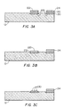
- Fig. 3A is a partial section view of a glass substrate illustrating a step of the method of the present invention;
- Fig. 3B is a view of the substrate of Fig. 3A illustrating a further step in the method of the present invention;
- Fig. 3C is a view of the substrate of Fig. 3B illustrating a further step in the method of the present invention;
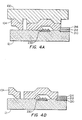
- Fig. 4A is a partial section view of the substrate of Fig. 3C disposed over the substrate of Fig. 2C according to the method of the present invention; and
- Fig. 4B is a view of the substrates of Fig. 4A illustrating a further step in the method of the present invention.
-
- The present invention contemplates a micromechanical
tuning fork gyroscope 10 fabricated by a dissolved silicon wafer process whereby electrostatic bonding forms a hermetic seal between anetched glass substrate 12, metal electrodes deposited thereon, and a silicon comb drivetuning fork gyroscope 14. The dissolved silicon wafer process involves single sided processing of a silicon substrate, including the steps of etching recesses, diffusing an etch resistant dopant into the silicon substrate, and releasing various components of the silicon gyroscope by etching through the diffusion layer in desired locations. The glass substrate also undergoes single sided processing, including the steps of etching recesses, depositing a multi-metal system in the recesses, and selectively etching portions of the multi-metal system. One substrate is inverted over the other and aligned before anodic bonding of the two substrates is performed. - In Fig. 1, one embodiment of a
comb drive gyroscope 14 fabricated according to the present invention is illustrated. The gyroscope thus formed employs drive 16 and drivenfinger electrodes 18 formed by plural respective interleavedfingers 24 for imparting vibrational motion to the tuningfork vibrating elements 20. The finger electrodes greatly increase the area and capacitance as well as the capacitance change with motion of the device so as to substantially enhance system sensitivity. Moreover, such an electrode structure is compatible with the dissolved silicon wafer process disclosed herein. Thetuning fork gyroscope 14 thus provides reduced parasitic capacitance resulting from the use of a glass substrate, reduced discrete processing steps with a resultant reduction in production cost and fabrication time, and enhanced resistance to adhesion between the silicon structure, the glass substrate and the metallic electrodes disposed therebetween. - It is understood that the process as described herein is applicable to the fabrication of various embodiments of micromechanical comb-drive gyroscopes other than that shown in Fig. 1. However, common features of these gyroscopes include the following elements. A first surface of a glass substrate has suspended thereover a
silicon rotatable assembly 30 comprising first and second vibratingassemblies 20 which extend from one or more anchors 32. The vibratingassemblies 20 are comprised of opposing comb structures made up of drivenelectrode fingers 24 extending therefrom. Disposed on the first surface of the glass substrate are cooperatingdrive electrode fingers 16 for alternating alignment with the drivenfinger electrodes 18.Torque 36, or rebalance, andsense electrodes 38 are disposed on the glass substrate beneath a portion of the vibrating assemblies and/or support structures extending between the vibrating assemblies and the anchors. Also disposed on the glass substrate are metallic conductive leads 40 interconnecting transducers with theelectrodes center drive motors 48. These transducers include left 50 andright torque transducers 52, left 54 andright sense transducers 56, andmotor transducer 58. - In short, the method of fabricating a
gyroscope 14 as depicted in Fig. 1 begins with reactive ion etching (RIE) and boron diffusion of silicon to define the suspended gyroscope structure. Specifically, with reference to Fig. 2A, processing starts with a p-type silicon wafer 100 of moderate doping (eg. >1Ω-cm).Recesses 102 etched into the silicon using potassium hydroxide (KOH) will eventually define the gap spacing of conducting elements which comprise the electrodes. Recesses may also be formed using RIE or plasma techniques. - As depicted in Fig. 2B, a high temperature (eg. 1150-1175°C) boron (p++)
diffusion 104 across the surface of the Si substrate follows. The diffusion depth, which may be in the range of 5 to 10 µm, defines the thickness of the resulting gyroscope structure. The outline of the features of the structure is defined by using RIE to etch past the p++ diffusedetch stop layer 104, thus releasing and uniquely defining individual elements of the structure as shown in Fig. 2C. Preferably, a CF3Br (trifluorobromomethane) chemistry is used for etching in a parallel plate reactor, thus resulting instraight sidewalls 106 and high aspect ratios. Other chemistries, such as BCl3/Cl2 (boron tri-chloride/chlorine) or HBr (hydrogen bromide), CF4 (carbon tetrafluoride), O2 (oxygen) chemical mixtures can also be used. - Therefore, it is the
boron diffusion 104 of Fig. 2B which defines the gyroscope thickness, and the RIE etching of Fig. 2C which defines the width of the gyroscope elements. - Glass processing is described with reference to Figs. 3A-3C. In Fig. 3A, a
glass wafer 12, such as a #7740 Corning glass wafer, is selectively etched to form low profilemetal deposition sites 200. Hydrofluoric acid or plasma (e.g. RIE) may be used as the glass etchant. Next, amulti-metal system 202 is deposited in the etched recesses. One embodiment of the present invention employs a titanium-platinum-gold (Ti-Pt-Au) combination for electrode and conductor structures.Titanium 210 is deposited in theglass wafer 12recess 200 first, for example to a thickness of 0.04 µm (400Å), due to its excellent adhesion to glass. Next,platinum 212 is deposited, for example to a depth of 0.07 µm (700Å), on thetitanium 210. Finally, a layer ofgold 214, 0.1 µm (1000Å) thick for example, is deposited on theplatinum 212. Thegold 214 makes a superior contact point for wire bonding. Employing these exemplary thicknesses produces a planar structure with metal protruding only 0.05 µm (500Å) above the surface of theglass 12. - The three metals do not alloy with each other, thus enabling electrostatic bonding taking place at approximately 375°C. The
platinum 212 further acts as an adhesion promoter between thegold 214 andtitanium 210. However,gold 214 is a soft metal which is subject to compression under moderate pressures (eg. >6666 Pa (>50 Torr)). - As stated, various embodiments of micromechanical, silicon on glass, comb-drive gyroscopes are known. The minimum electrode gap between silicon devices and metal electrodes in these embodiments is ideally reduced to enable the use of higher magnitude drive forces and larger amplitude vibrations, which in turn increases gyroscope sensitivity. Electrode gap is further minimized to enable operation of gyroscopes under higher pressures. As a result of the gap minimization, "sticking" may occur; such adhesion of the silicon resonant mass to an underlying gold or other soft metal electrode can render the rate sensing device useless.
- To overcome this negative aspect of micromechanical tuning fork gyroscopes, one gyroscope embodiment according to the present invention has gold replaced with a metal which is chemically stable (so that chemical reactions do not aic adhesion), which is resistant to compression, and which is resistant to EDP.
Platinum 212 fulfills all these requirements, and thus is ideally suited for being anupper surface 220 of electrodes which are subject to high force silicon impact, as illustrated in Fig. 3B. It is recognized that other metals can be substituted for platinum due tc their similar properties. For example, suitable metals are in the refractory, silicide, and nobel metal categories, such as tungsten, molybdenum, titanium-tungsten (TiW), paladium, iridium, tungsten silicide, and titanium silicide. However, in certain embodiments of the gyroscope, gold and gold combinations (e.g. titanium gold, platinum gold) are acceptable. - Another aspect in addressing the problem of adhesion or sticking is the vertical stiffness per contact area betweer the two contacting materials. If the contact area is reduced, then the effective sticking force can also be reduced. This is accomplished in the present invention by etching away the
gold 214 from areas likely to come into contact with the suspended silicon device, such as at electrodes. The underlying platinum is masked and etched to form posts or stand-offs, thus reducing the total contact area, as illustrated in Fig. 3C. A suitable etchant for removal of the gold layer is iodine-based solutions. - While it is beneficial to minimize the number of stand-
offs 230, too few allow the impacting silicon to drape over the stand-offs and contact the remaining platinum or exposed titanium sheet, thus increasing adhesive tendency. Four stand-offs in a square configuration act as corners for a free standing membrane; in effect, the area between the four corner stand-offs acts as a pressure sensor. The stiffness of these regions is based on plate bending theory. The linear spacing between stand-offs, dmax, is given by: - E = Young's Modulus
- t = plate thickness
- h = gap spacing
- Θ = contact angle
- ν = Poisson's ratio
- α = 0.00581
- γ 1 = surface tension (72mJ/m2) According to an exemplary embodiment, for a 0.3µm high standoff, dmax is 118µm.
-
- One embodiment of the present invention as described and illustrated has platinum stand-
offs 230. However, it should be understood that a planar layer of platinum will suffice for adhesion resistance in some gyroscope applications in light of the beneficial physical characteristics of platinum already discussed and the low profile of the metal conductors with respect to the silicon gyroscope structure suspended thereover. - In addition, the present invention has been described as employing a solid
glass wafer substrate 12. The impact of any thermal mismatch between the silicon structure and glass substrate may be minimized by a relatively thick silicon structure. However, the benefits of a glass substrate, i.e. reduction in stray capacitance and ability of amorphous glass to bond over uneven silicon wafer surfaces and stray particulate, may be achieved by employing glass sputtered on a silicon wafer. Such a substrate would reduce a likelihood of thermal mismatch while still providing the aforementioned benefits resulting from anodic bonding of glass to silicon. Further, with a thinner layer of glass to be bound, low temperature anodic bonding is employed. - After processing of the
individual silicon 100 andglass wafers 12, one wafer is inverted over the other and aligned as shown in Figs. 4A-4B. The glass and silicon structures are electrostatically bonded at, for example, 375°C with a potential of approximately 1000V applied between the glass and silicon. A compression bond is formed between thegold 214, deposited on theglass substrate 12, and thesilicon 100, which then sinter forming chemically bonded, electrically conductive, low-resistance leads (eg. 40Ω for a 40µm x 20µm area). - The final step in the process is a selective etch in ethylene-diamine-pyrocatechol-water (EDP). EDP dissolves the
silicon substrate 100 but stops at the heavily doped (p++) diffused layers 104. Other selective silicon etchants such as potassium hydroxide, hydraline, and hydrofluoric acid-nitric acid-acetic acid solutions are alternatives for silicon dissolving. Thus the overall fabrication sequence involves only single-sided processing with a minimum number of masking steps on silicon, one diffusion step into silicon, and one masking step on glass. The present process is both high yield and compatible with batch processing.
Claims (25)
- A method for fabricating a comb drive tuning fork gyroscope, including associated electrodes, transducers, and interconnecting electrical leads, said gyroscope adapted for inertial rate sensitivity, comprising the steps of:providing a silicon substrate having a first surface;forming discrete elements of said gyroscope in selected regions of said first surface of said silicon substrate;providing a glass substrate having a first surface;forming a plurality of multilayer metal deposits in a plurality of recessed regions of said first surface of said glass substrate;removing selected portions of said multilayer metal deposit from selected ones of said plurality of recessed regions so as to overcome the negative aspect of sticking;bonding said first surface of said silicon substrate to said first surface of said glass substrate; andexposing said silicon substrate to an etchant.
- The method of claim 1 wherein said step of forming gyroscope elements includes the steps of:forming a plurality of raised regions in said first surface of said silicon substrate;forming a doped region and an undoped region in said silicon substrate by diffusing into said silicon substrate first surface a dopant resistant to a silicon etchant; andremoving selected portions of said first surface of said silicon substrate to define said discrete elements of said gyroscope.
- The method of claim 1 wherein said step of forming multilayer metal deposits includes the steps of:etching said first surface of said glass substrate to form a plurality of recessed regions; andforming in each of said recessed regions of said glass substrate said plurality of multilayer metal deposits by successive depositions of individual conductive metal layers.
- The method of claim 1 wherein said step of removing selected portions of said multilayer metal deposit includes the steps of:
etching through a first metallic layer to expose a planar surface of a second layer. - The method of claim 1 wherein said step of removing selected portions of said multilayer metal deposit includes the steps of:
etching a first metallic layer to form a plurality of stand-offs. - The method of claim 5 wherein said step of etching through said first metallic layer includes the steps of:masking said first metallic layer; andexposing said masked first metallic layer to an etchant.
- The method of claim 6 wherein said step of etching said first metallic layer forms a regularly spaced array of said stand-offs in said first layer.
- The method of claim 5 wherein said step of etching through said first metallic layer includes the steps of:etching through said first metallic layer to expose a second metallic layer;masking said second metallic layer; andetching said second metallic layer.
- The method of claim 8 wherein said step of etching said second metallic layer forms a regularly spaced array of said stand-offs in said second layer.
- The method of claim 8 wherein said step of etching said second metallic layer includes the step of exposing a third metallic layer from which said plurality of stand-offs extend.
- The method of claim 8 wherein said step of etching said second metallic layer includes the step of forming a planar surface of said second metallic layer from which said plurality of stand-offs extend.
- The method of claim 1 wherein said step of bonding said first surface of said silicon substrate to said first surface of said glass substrate includes the steps of:inverting one of said silicon substrate and said glass substrate;disposing said substrates in an aligned orientation; andbonding said substrates together.
- The method of claim 12 wherein said step of bonding includes the step of anodically bonding the substrates.
- A method for forming a micromechanical tuning fork structure adapted for use in rate sensor applications comprising the steps of:providing a silicon substrate having a planar first surface;forming a height varying pattern in said first surface of said silicon substrate;exposing said first surface of said silicon substrate to a silicon dopant for a discrete time period;removing selected portions of said silicon substrate;providing a second substrate having a planar first surface, said first surface of said second substrate comprised of glass;forming a plurality of recesses in said first surface of said second substrate;depositing a plurality of superimposed metallic layers in said plurality of recesses;removing a first metallic layer to expose a second metallic layer from at least one of said plurality of recesses so as to overcome the negative aspect of sticking;disposing said first surface of said silicon substrate against said first surface of said second substrate; andremoving a second surface of said silicon substrate not exposed to said silicon dopant.
- The method of claim 14 wherein said step of forming a height varying pattern in said first surface of said silicon substrate includes the step of etching said first surface of said silicon substrate using potassium hydroxide or plasma techniques.
- The method of claim 14 wherein said step of exposing said first surface of said silicon substrate includes the step of diffusing boron into said first surface of said silicon substrate.
- The method of claim 14 wherein said step of removing selected portions of said silicon substrate includes using trifluorobromomethane chemistry in a parallel plate reactor.
- The method of claim 14 wherein said step of providing a second substrate includes the step of providing a second substrate comprised of glass.
- The method of claim 14 wherein said step of providing a second substrate includes the step of providing a second substrate on which a deposition of glass has been sputtered.
- The method of claim 14 wherein said step of forming a plurality of recesses in said first surface of said second substrate includes the step of etching said second substrate using hydrofluoric acid or plasma techniques.
- The method of claim 14 wherein said step of depositing a plurality of superimposed metallic layers in said plurality of recesses includes the step of sequentially depositing a third substrate of titanium, a second substrate of platinum, and a first substrate of gold.
- The method of claim 14 wherein said step of removing a first metallic layer to expose a second metallic layer includes the steps of:etching said first metallic layer;masking said second metallic layer; andetching said second metallic layer.
- The method of claim 22 wherein said step of etching said second metallic layer forms a plurality of stand-offs extending from said second metallic layer.
- The method of claim 14 wherein said step of disposing said first surface of said silicon substrate against said first surface of said second substrate includes the step of anodically bonding said first and second surfaces together.
- The method of claim 14 wherein said step of removing a second surface of said silicon substrate includes the step of exposing said second surface to ethylene-diamine-pyrocatechol-water.
Applications Claiming Priority (3)
| Application Number | Priority Date | Filing Date | Title |
|---|---|---|---|
| US191979 | 1980-09-29 | ||
| US08/191,979 US5492596A (en) | 1994-02-04 | 1994-02-04 | Method of making a micromechanical silicon-on-glass tuning fork gyroscope |
| PCT/US1995/001330 WO1995021383A1 (en) | 1994-02-04 | 1995-02-01 | Method of making a micromechanical silicon-on-glass tuning fork gyroscope |
Publications (3)
| Publication Number | Publication Date |
|---|---|
| EP0742904A1 EP0742904A1 (en) | 1996-11-20 |
| EP0742904A4 EP0742904A4 (en) | 1998-07-15 |
| EP0742904B1 true EP0742904B1 (en) | 2001-04-25 |
Family
ID=22707712
Family Applications (1)
| Application Number | Title | Priority Date | Filing Date |
|---|---|---|---|
| EP95909430A Expired - Lifetime EP0742904B1 (en) | 1994-02-04 | 1995-02-01 | Method of making a micromechanical silicon-on-glass tuning fork gyroscope |
Country Status (6)
| Country | Link |
|---|---|
| US (1) | US5492596A (en) |
| EP (1) | EP0742904B1 (en) |
| JP (1) | JP3508025B2 (en) |
| CA (1) | CA2181993C (en) |
| DE (1) | DE69520785T2 (en) |
| WO (1) | WO1995021383A1 (en) |
Families Citing this family (48)
| Publication number | Priority date | Publication date | Assignee | Title |
|---|---|---|---|---|
| DE4414237A1 (en) * | 1994-04-23 | 1995-10-26 | Bosch Gmbh Robert | Micromechanical vibrator of an oscillation gyrometer |
| KR100374803B1 (en) * | 1995-05-25 | 2003-05-12 | 삼성전자주식회사 | Tuning Fork Gyroscopes |
| US5914801A (en) | 1996-09-27 | 1999-06-22 | Mcnc | Microelectromechanical devices including rotating plates and related methods |
| KR100408530B1 (en) * | 1996-10-31 | 2004-01-24 | 삼성전자주식회사 | A method for fabricating a microgyroscope |
| KR100231711B1 (en) * | 1996-12-20 | 1999-11-15 | 양승택 | How to make a micro gyroscope |
| KR100233848B1 (en) * | 1996-12-21 | 1999-12-01 | 정선종 | Manufacturing method of micro-gyroscope |
| KR100442824B1 (en) * | 1997-05-12 | 2004-09-18 | 삼성전자주식회사 | A micromachine and a method for fabricating the same |
| US6232150B1 (en) | 1998-12-03 | 2001-05-15 | The Regents Of The University Of Michigan | Process for making microstructures and microstructures made thereby |
| JP3119255B2 (en) * | 1998-12-22 | 2000-12-18 | 日本電気株式会社 | Micromachine switch and method of manufacturing the same |
| KR100316774B1 (en) * | 1999-01-15 | 2001-12-12 | 이형도 | Method for fabricating a micro inertia sensor |
| KR100506074B1 (en) * | 1999-01-15 | 2005-08-04 | 삼성전자주식회사 | Decoupled Z-axis gyroscope and fabricating method thereof |
| US6189381B1 (en) | 1999-04-26 | 2001-02-20 | Sitek, Inc. | Angular rate sensor made from a structural wafer of single crystal silicon |
| US6275320B1 (en) | 1999-09-27 | 2001-08-14 | Jds Uniphase, Inc. | MEMS variable optical attenuator |
| US6770503B1 (en) * | 1999-10-21 | 2004-08-03 | The Charles Stark Draper Laboratory, Inc. | Integrated packaging of micromechanical sensors and associated control circuits |
| US6373682B1 (en) | 1999-12-15 | 2002-04-16 | Mcnc | Electrostatically controlled variable capacitor |
| US6677225B1 (en) * | 2000-07-14 | 2004-01-13 | Zyvex Corporation | System and method for constraining totally released microcomponents |
| US6544810B1 (en) | 2000-08-31 | 2003-04-08 | Motorola, Inc. | Capacitively sensed micromachined component and method of manufacturing |
| US6485273B1 (en) | 2000-09-01 | 2002-11-26 | Mcnc | Distributed MEMS electrostatic pumping devices |
| US6590267B1 (en) | 2000-09-14 | 2003-07-08 | Mcnc | Microelectromechanical flexible membrane electrostatic valve device and related fabrication methods |
| US6377438B1 (en) | 2000-10-23 | 2002-04-23 | Mcnc | Hybrid microelectromechanical system tunable capacitor and associated fabrication methods |
| US6396620B1 (en) | 2000-10-30 | 2002-05-28 | Mcnc | Electrostatically actuated electromagnetic radiation shutter |
| DE10055081A1 (en) * | 2000-11-07 | 2002-05-16 | Bosch Gmbh Robert | Micro-component used as a sensor element comprises a glass body provided with an electrically conducting coating on its side facing a microstructure |
| US6808956B2 (en) * | 2000-12-27 | 2004-10-26 | Honeywell International Inc. | Thin micromachined structures |
| US6582985B2 (en) | 2000-12-27 | 2003-06-24 | Honeywell International Inc. | SOI/glass process for forming thin silicon micromachined structures |
| US6862934B2 (en) * | 2001-10-05 | 2005-03-08 | The Charles Stark Draper Laboratory, Inc. | Tuning fork gyroscope |
| US20040073175A1 (en) * | 2002-01-07 | 2004-04-15 | Jacobson James D. | Infusion system |
| US6877374B2 (en) * | 2002-02-06 | 2005-04-12 | Analog Devices, Inc. | Micromachined gyroscope |
| US7089792B2 (en) * | 2002-02-06 | 2006-08-15 | Analod Devices, Inc. | Micromachined apparatus utilizing box suspensions |
| AU2003226083A1 (en) * | 2002-03-26 | 2003-10-13 | The Charles Stark Draper Laboratory, Inc. | Microelectromechanical sensors having reduced signal bias errors and methods of manufacturing the same |
| US6908791B2 (en) * | 2002-04-29 | 2005-06-21 | Texas Instruments Incorporated | MEMS device wafer-level package |
| US20040065638A1 (en) * | 2002-10-07 | 2004-04-08 | Bishnu Gogoi | Method of forming a sensor for detecting motion |
| US6770504B2 (en) * | 2003-01-06 | 2004-08-03 | Honeywell International Inc. | Methods and structure for improving wafer bow control |
| US6888233B2 (en) * | 2003-03-10 | 2005-05-03 | Honeywell International Inc. | Systems for buried electrical feedthroughs in a glass-silicon MEMS process |
| US20050062362A1 (en) * | 2003-08-28 | 2005-03-24 | Hongyuan Yang | Oscillatory gyroscope |
| JP4512636B2 (en) * | 2004-04-14 | 2010-07-28 | アナログ デバイシス, インコーポレイテッド | Inertial sensor with linearly arrayed sensor elements |
| US7153759B2 (en) * | 2004-04-20 | 2006-12-26 | Agency For Science Technology And Research | Method of fabricating microelectromechanical system structures |
| CA2571829A1 (en) * | 2004-07-23 | 2006-02-02 | Afa Controls, Llc | Methods of operating microvalve assemblies and related structures and related devices |
| US7370530B2 (en) * | 2004-09-01 | 2008-05-13 | Honeywell International Inc. | Package for MEMS devices |
| US7478557B2 (en) * | 2004-10-01 | 2009-01-20 | Analog Devices, Inc. | Common centroid micromachine driver |
| US7300814B2 (en) * | 2004-12-16 | 2007-11-27 | The Charles Stark Draper Laboratory, Inc. | Method for fabricating micro-mechanical devices |
| FI116543B (en) * | 2004-12-31 | 2005-12-15 | Vti Technologies Oy | Oscillating micro-mechanical angular velocity sensor, for vehicle, has seismic masses that are connected to support areas using springs or auxiliary structures |
| US7302848B2 (en) | 2005-03-10 | 2007-12-04 | The Charles Stark Draper Laboratory, Inc. | Force compensated comb drive |
| US7421897B2 (en) | 2005-04-14 | 2008-09-09 | Analog Devices, Inc. | Cross-quad and vertically coupled inertial sensors |
| US7426861B2 (en) | 2005-06-15 | 2008-09-23 | The Charles Stark Draper Laboratory, Inc. | Tuning fork gyroscopes, accelerometers, and other sensors with improved scale factor |
| JP2008135690A (en) * | 2006-10-30 | 2008-06-12 | Denso Corp | Semiconductor dynamic quantity sensor and manufacturing method thereof |
| US8187902B2 (en) * | 2008-07-09 | 2012-05-29 | The Charles Stark Draper Laboratory, Inc. | High performance sensors and methods for forming the same |
| ITTO20120542A1 (en) | 2012-06-20 | 2013-12-21 | St Microelectronics Srl | MICROELETTROMECHANICAL DEVICE WITH SIGNAL INSERTION THROUGH A PROTECTIVE HOOD AND METHOD FOR CHECKING A MICROELECTROMECHANICAL DEVICE |
| JP2020139879A (en) * | 2019-02-28 | 2020-09-03 | セイコーエプソン株式会社 | Inertia sensors, electronics and moving objects |
Family Cites Families (11)
| Publication number | Priority date | Publication date | Assignee | Title |
|---|---|---|---|---|
| US4654663A (en) * | 1981-11-16 | 1987-03-31 | Piezoelectric Technology Investors, Ltd. | Angular rate sensor system |
| US4764244A (en) * | 1985-06-11 | 1988-08-16 | The Foxboro Company | Resonant sensor and method of making same |
| US5013396A (en) * | 1987-06-01 | 1991-05-07 | The Regents Of The University Of Michigan | Method of making an ultraminiature pressure sensor |
| US4815472A (en) * | 1987-06-01 | 1989-03-28 | The Regents Of The University Of Michigan | Multipoint pressure-sensing catheter system |
| US4881410A (en) * | 1987-06-01 | 1989-11-21 | The Regents Of The University Of Michigan | Ultraminiature pressure sensor and method of making same |
| US5216490A (en) * | 1988-01-13 | 1993-06-01 | Charles Stark Draper Laboratory, Inc. | Bridge electrodes for microelectromechanical devices |
| US5055838A (en) * | 1988-12-09 | 1991-10-08 | The Regents Of The University Of Michigan | Silicon tactile imaging array and method of making same |
| DE4009090A1 (en) * | 1990-03-21 | 1991-09-26 | Bosch Gmbh Robert | METHOD FOR PRODUCING MULTILAYER SILICON STRUCTURES |
| DE4012080A1 (en) * | 1990-04-14 | 1991-10-17 | Bosch Gmbh Robert | METHOD FOR BUILDING MICROMECHANICAL SENSORS |
| US5329815A (en) * | 1991-12-19 | 1994-07-19 | Motorola, Inc. | Vibration monolithic gyroscope |
| US5313835A (en) * | 1991-12-19 | 1994-05-24 | Motorola, Inc. | Integrated monolithic gyroscopes/accelerometers with logic circuits |
-
1994
- 1994-02-04 US US08/191,979 patent/US5492596A/en not_active Expired - Lifetime
-
1995
- 1995-02-01 JP JP52072795A patent/JP3508025B2/en not_active Expired - Lifetime
- 1995-02-01 CA CA002181993A patent/CA2181993C/en not_active Expired - Lifetime
- 1995-02-01 DE DE69520785T patent/DE69520785T2/en not_active Expired - Lifetime
- 1995-02-01 WO PCT/US1995/001330 patent/WO1995021383A1/en not_active Ceased
- 1995-02-01 EP EP95909430A patent/EP0742904B1/en not_active Expired - Lifetime
Also Published As
| Publication number | Publication date |
|---|---|
| DE69520785D1 (en) | 2001-05-31 |
| CA2181993A1 (en) | 1995-08-10 |
| EP0742904A1 (en) | 1996-11-20 |
| DE69520785T2 (en) | 2001-08-30 |
| EP0742904A4 (en) | 1998-07-15 |
| JPH09511571A (en) | 1997-11-18 |
| WO1995021383A1 (en) | 1995-08-10 |
| JP3508025B2 (en) | 2004-03-22 |
| CA2181993C (en) | 2001-01-16 |
| US5492596A (en) | 1996-02-20 |
Similar Documents
| Publication | Publication Date | Title |
|---|---|---|
| US5492596A (en) | Method of making a micromechanical silicon-on-glass tuning fork gyroscope | |
| US5496436A (en) | Comb drive micromechanical tuning fork gyro fabrication method | |
| US6817725B2 (en) | Micro mirror unit and method of making the same | |
| KR101168353B1 (en) | Thin film precursor stack for mems manufacturing | |
| US5889207A (en) | Micromechanical rate of rotation sensor having ring with drive element and detection element | |
| US6445053B1 (en) | Micro-machined absolute pressure sensor | |
| US20090302716A1 (en) | Piezoelectric device | |
| WO1989008847A1 (en) | Differential capacitive transducer and method | |
| GB2276976A (en) | A Method of manufacturing a motion sensor | |
| US6706549B1 (en) | Multi-functional micro electromechanical devices and method of bulk manufacturing same | |
| EP0664438B1 (en) | Comb drive micromechanical tuning fork gyro | |
| EP0816856A1 (en) | Electrosatatic capacitive sensor and method for manufacturing the same | |
| CN118190238B (en) | Gas pressure sensor chip based on semiconductor film and preparation method thereof | |
| JP3156453B2 (en) | Semiconductor capacitive acceleration sensor | |
| JPH10163505A (en) | Semiconductor inertial sensor and method of manufacturing the same | |
| JPH10178183A (en) | Semiconductor inertial sensor and method of manufacturing the same | |
| EP1544165A2 (en) | Method for gyroscope using SMS wafer and gyroscope fabricated by the same | |
| JPH10270719A (en) | Semiconductor inertial sensor and method of manufacturing the same | |
| JP3287287B2 (en) | Distortion detecting element and method of manufacturing the same | |
| JPH10178181A (en) | Manufacturing method of semiconductor inertial sensor | |
| JPH11214706A (en) | Semiconductor sensor and method of manufacturing the same | |
| JP2819995B2 (en) | Capacitive weight sensor element and method of manufacturing the same | |
| KR100825626B1 (en) | Microstructure | |
| JPH07263712A (en) | Semiconductor sensor | |
| JPH10178184A (en) | Semiconductor inertial sensor and method of manufacturing the same |
Legal Events
| Date | Code | Title | Description |
|---|---|---|---|
| PUAI | Public reference made under article 153(3) epc to a published international application that has entered the european phase |
Free format text: ORIGINAL CODE: 0009012 |
|
| 17P | Request for examination filed |
Effective date: 19960805 |
|
| AK | Designated contracting states |
Kind code of ref document: A1 Designated state(s): DE FR GB |
|
| A4 | Supplementary search report drawn up and despatched |
Effective date: 19980526 |
|
| AK | Designated contracting states |
Kind code of ref document: A4 Designated state(s): DE FR GB |
|
| GRAG | Despatch of communication of intention to grant |
Free format text: ORIGINAL CODE: EPIDOS AGRA |
|
| 17Q | First examination report despatched |
Effective date: 20000727 |
|
| GRAG | Despatch of communication of intention to grant |
Free format text: ORIGINAL CODE: EPIDOS AGRA |
|
| GRAH | Despatch of communication of intention to grant a patent |
Free format text: ORIGINAL CODE: EPIDOS IGRA |
|
| GRAH | Despatch of communication of intention to grant a patent |
Free format text: ORIGINAL CODE: EPIDOS IGRA |
|
| GRAA | (expected) grant |
Free format text: ORIGINAL CODE: 0009210 |
|
| AK | Designated contracting states |
Kind code of ref document: B1 Designated state(s): DE FR GB |
|
| REF | Corresponds to: |
Ref document number: 69520785 Country of ref document: DE Date of ref document: 20010531 |
|
| ET | Fr: translation filed | ||
| REG | Reference to a national code |
Ref country code: GB Ref legal event code: IF02 |
|
| PLBE | No opposition filed within time limit |
Free format text: ORIGINAL CODE: 0009261 |
|
| STAA | Information on the status of an ep patent application or granted ep patent |
Free format text: STATUS: NO OPPOSITION FILED WITHIN TIME LIMIT |
|
| 26N | No opposition filed | ||
| PGFP | Annual fee paid to national office [announced via postgrant information from national office to epo] |
Ref country code: DE Payment date: 20140129 Year of fee payment: 20 |
|
| PGFP | Annual fee paid to national office [announced via postgrant information from national office to epo] |
Ref country code: FR Payment date: 20140211 Year of fee payment: 20 |
|
| PGFP | Annual fee paid to national office [announced via postgrant information from national office to epo] |
Ref country code: GB Payment date: 20140129 Year of fee payment: 20 |
|
| REG | Reference to a national code |
Ref country code: DE Ref legal event code: R071 Ref document number: 69520785 Country of ref document: DE |
|
| REG | Reference to a national code |
Ref country code: GB Ref legal event code: PE20 Expiry date: 20150131 |
|
| PG25 | Lapsed in a contracting state [announced via postgrant information from national office to epo] |
Ref country code: GB Free format text: LAPSE BECAUSE OF EXPIRATION OF PROTECTION Effective date: 20150131 |