EP0742587B1 - Apparatus and method for semiconductor wafer edge inspection - Google Patents
Apparatus and method for semiconductor wafer edge inspection Download PDFInfo
- Publication number
- EP0742587B1 EP0742587B1 EP96302674A EP96302674A EP0742587B1 EP 0742587 B1 EP0742587 B1 EP 0742587B1 EP 96302674 A EP96302674 A EP 96302674A EP 96302674 A EP96302674 A EP 96302674A EP 0742587 B1 EP0742587 B1 EP 0742587B1
- Authority
- EP
- European Patent Office
- Prior art keywords
- wafers
- edges
- wafer
- light
- holder
- Prior art date
- Legal status (The legal status is an assumption and is not a legal conclusion. Google has not performed a legal analysis and makes no representation as to the accuracy of the status listed.)
- Expired - Lifetime
Links
Images


Classifications
-
- H—ELECTRICITY
- H10—SEMICONDUCTOR DEVICES; ELECTRIC SOLID-STATE DEVICES NOT OTHERWISE PROVIDED FOR
- H10P—GENERIC PROCESSES OR APPARATUS FOR THE MANUFACTURE OR TREATMENT OF DEVICES COVERED BY CLASS H10
- H10P74/00—Testing or measuring during manufacture or treatment of wafers, substrates or devices
-
- H—ELECTRICITY
- H10—SEMICONDUCTOR DEVICES; ELECTRIC SOLID-STATE DEVICES NOT OTHERWISE PROVIDED FOR
- H10P—GENERIC PROCESSES OR APPARATUS FOR THE MANUFACTURE OR TREATMENT OF DEVICES COVERED BY CLASS H10
- H10P74/00—Testing or measuring during manufacture or treatment of wafers, substrates or devices
- H10P74/20—Testing or measuring during manufacture or treatment of wafers, substrates or devices characterised by the properties tested or measured, e.g. structural or electrical properties
- H10P74/203—Structural properties, e.g. testing or measuring thicknesses, line widths, warpage, bond strengths or physical defects
Definitions
- This invention relates generally to the inspection of semiconductor wafers used to make computer chips and, more particularly, to a method of and apparatus for inspecting the edges of a plurality of such wafers in a single operation.
- edge inspection has involved using a bright light to illuminate the edge of an individual wafer, rotating the wafer (held in a horizontal position on a chuck) under the light, and visually observing scattering or other distortion of the light indicative of a defect in the edge. This procedure has been carried out for each individual wafer, making inspection very time consuming and costly.
- Patent Abstracts of Japan, Vol 016, No. 486 (E-1276) and JP-A-04/177851 disclose inspection of the edge of a single wafer by illuminating the edge with light, whereafter transmitted light is detected.
- Patent Abstracts of Japan, Vol. 095, No. 001, 28 February 1995, and JP-A 06/302676 also disclose inspection of the edge of a single wafer by illuminating its edge, the reflected light being detected.
- the present invention is directed to an improved method of and apparatus for carrying out the wafer edge inspection process.
- an improved method of and apparatus for inspecting the edges of a plurality of wafers e.g., up to 25
- the provision of such apparatus which is capable of inspecting wafers of different diameters and which can be rapidly converted between a mode for inspecting wafers of one diameter and a mode for inspecting wafers of a different diameter
- the provision of such apparatus which is economical to manufacture and easy to operate
- the provision of such apparatus which protects the wafers during the inspection process
- the provision of such a method which also provides the advantages noted above.
- apparatus for inspecting a plurality of semiconductor wafers is shown to include a support system, indicated generally at 10, supporting a wafer cassette 12 holding the semiconductor wafers W.
- the wafer cassette 12 is of conventional construction, having an open top, an open bottom and a series of partitions inside the cassette defining a plurality of parallel slots 14 (Fig. 2) for holding semiconductor wafers W of the same diameter.
- Each wafer slot 14 is adapted to hold a single wafer W extending from the slot above the open top of the cassette 12.
- the wafers W are held by the cassette 12 in spaced apart parallel relation, each wafer having a center and a generally circular outer edge E.
- the wafers W are formed so that the edges each have a short segment (not shown) which is straight for purposes of orienting the wafers.
- the wafers W are generally circular.
- the wafer cassette 12 holds the wafers W with their centers substantially on a common axis and their edges E substantially in alignment.
- a light source is capable of projecting a well-defined columnar beam of light B (illustrated by parallel lines in Figs. 1 and 2) along a central longitudinal axis generally parallel to the common axis of the wafers W and generally tangential to the edges E of the wafers in the cassette 12 to illuminate the edges.
- the light source 16 includes a housing 18 which is mounted by a stand (generally indicated at 20) at a predetermined height.
- a projection lamp (not shown) having a brightness of about 21,000 foot candles (226042 lumens/m 2 ) is located in the housing and provides the beam of light B. It has been found that a brightness of 18,000 foot candles (193750 lumens/m 2 ) produces satisfactory results.
- the stand 20 includes a post 22 mounted on and projecting up from a base plate 24 of the apparatus, and a pivoting mount including a vertical member 28 connected to the post and a horizontal member 30 extending from the vertical member to the housing 18.
- the horizontal member 30 is capable of pivoting about a horizontal axis relative to the vertical member 28 and post 22 to change the angle of the beam of light B so as to maintain the beam tangential to the upper portions of the edges E of the wafers W.
- the horizontal member 30 is capable of being fixed in a selected angular position by suitable locking devices, such as set screws (not shown).
- the wafers W in the wafer cassette 12 engage a roller 34 and the wafer cassette rests on a frame 36 of a wafer rotating device (indicated generally at 38) supported by the support system 10.
- the wafer rotating device 38 is of a conventional construction, having an axle 40 mounting the roller 34 which extends outwardly from the frame 36 to a hand grip 42.
- Wafer rotating devices of the same type as wafer rotating device 38 are used for orienting the wafers W in the cassette so that the straight portion of the edge E is at the bottom.
- the roller 34 is located below the open bottom of the cassette 12 and its outer surface engages the edges E of the wafers in the cassette so that rotation of the roller causes the wafers W to rotate in an opposite direction within the wafer cassette.
- the wafer cassette 12 is made of a suitable low-friction material (e.g., Teflon® or polypropylene) to minimize wear on the wafers W as they rotate in their respective slots 14.
- the support system 10 comprises a platform, indicated generally at 48, including a pair of legs 50A, 50B fastened by bolts 52 to the base plate 24 and holding in cantilever fashion a support plate 54 extending rearwardly and at a downward angle from the legs. Spaced rearwardly from the rear edge of the support plate 54 are a pair of standoffs 56A, 56B connected to the base plate 24 by bolts 58. A forward facing surface 60A, 60B of each standoff 56A, 56B is sloped at an angle which is complementary to the angle the top surface of the support plate 54.
- An upstanding side plate 62 attached by bolts 64 to the leg 50B and the standoff 56B provides a guide surface against which the wafer cassette 12 may rest to be properly positioned.
- a slot 66 in the side plate 62 facilitates placing the wafer cassette 12, the wafer rotating device 38 and other elements of the support system 10 (described hereinafter) on the support plate 54.
- the support system 10 further includes a riser generally indicated at 66 in Figs. 5A and 5B, comprising a pair of laterally spaced side members 66A, 66B and a top member 66C extending between and connecting the side members.
- the support system 10 also includes a shorter riser, indicated generally at 68, which is shown in Figs. 6A-6B to comprise a pair of laterally spaced side members 68A, 68B and a top member 68C extending between and connecting the side members.
- Use of the risers 66, 68 permits the apparatus to be easily reconfigured in different modes for inspecting wafers of different diameters.
- the difference between the riser 66 shown in Figs. 5A and 5B and the riser 68 shown in Figs. 6A and 6B is the height of their side members (66A, 66B and 68A, 68B).
- the side members of the risers 66, 68 are each formed at their rearward ends with a downwardly projecting tail 70 which is snugly received between the rear edge of the support plate 54 and the forwardly facing surfaces 60A, 60B of the standoffs 56A, 56B.
- engagement of the side members 66A, 66B with the standoffs 56A, 56B holds the riser 66 from sliding down the sloped support plate 54 on which it rests.
- Generally L-shaped notches 72 in the upper rear edges of the side members 66A, 66B, 68A, 68B may receive either a rear portion of the wafer rotating device frame 36 (Fig.
- the support system 10 of the present invention may include additional risers (not shown) or no risers, and still fall within the scope of the present invention.
- Inspection of the wafers W using the apparatus of the present invention begins by determining whether one or more risers 66, 68 will be needed to hold upper portions of the edges E of the wafers at a position which will be generally tangential to the beam of light B to be projected from the light source 16. The determination will depend upon the diameter of the wafers W to be inspected. Assuming it is determined that the riser 66 is needed, it is placed on the support plate 54 of the platform and the wafer rotating device 38 is stacked upon the riser. It is to be understood that for large diameter wafers, no riser would be used and the wafer rotating device 38 would rest directly on the support plate 54 of the platform.
- the wafer cassette 12 will have been previously loaded with the polished surfaces of all the wafers W in the cassette facing in one direction and the unpolished surfaces facing in the other direction.
- the wafer cassette 12 is placed on the riser 66 so that the polished surfaces face toward the light source 16 and the unpolished surfaces face away from the light source.
- the cassette 12 is tipped back so that the weight of the wafers W is largely supported by engagement of the unpolished surfaces of the wafers with the cassette in the slots 14. In this way, there is little opportunity for wear or other damage to the wafers W as they are rotated within the cassette 12.
- the portions of the edges E of the wafers located at the open bottom of the cassette 12 engage the roller 34 so that rotation of the roller by turning the hand grip 42 will cause the wafers W to rotate in an opposite direction.
- the light source 16 is energized so that the light beam B is projected generally tangentially to the edges E of the wafers W above the cassette 12.
- the housing 18 of the light source may be pivoted relative to the vertical member 28 and post 22 by releasing and turning the horizontal member 30 of the stand 20.
- inspection of the edges E of the wafers is made visually from a position P above and forward of the location where the beam of light B is emitted from the housing 18. It will be noted that portions of the vertical member 28 and horizontal member 30 have been broken away in Fig. 2 to show the beam B continuously from the housing 18 to the wafers W.
- the inspector By turning the hand grip 42, the inspector brings new portions of the edges E of the wafers into tangential relationship with the beam of light B. In this way, the inspector may inspect the entire circumference of all of the wafers W from a single vantage point with a simple manipulation of the apparatus.
- edges E of the wafers W which do not have a defect produce a diffused back scattering of the light in the beam B readily recognized by skilled inspectors.
- the presence of a defect in an edge E of one of the wafers W will cause a back scattering of light which can be observed by the inspector at position P as a point of light on the wafer edge.
- the back scattering of light from the beam B caused by a defect is diagrammatically illustrated by lines L in Fig. 2.
- the inspector may then remove the defective wafer or mark the wafer as having an edge defect. It has been found to be practical to inspect 25 wafers at a time for edge defects using the apparatus and method of the present invention. The limitation of 25 wafers arises only because the largest industry standard wafer carrier is sized to hold 25 wafers.
- Edge inspection of wafers W can be carried out rapidly because multiple wafers can be inspected at a single time by an inspector using the columnar beam of light from the light source 16 directed tangentially to upper portions of the edges of the wafers.
- the wafers W can be held by the apparatus so that their weight is supported primarily on their unpolished surfaces, thereby protecting the polished surfaces.
- the apparatus can include risers 66, 68 which make the apparatus capable of quick reconfiguration for inspecting wafers of different diameters.
Landscapes
- Investigating Materials By The Use Of Optical Means Adapted For Particular Applications (AREA)
- Testing Or Measuring Of Semiconductors Or The Like (AREA)
- Container, Conveyance, Adherence, Positioning, Of Wafer (AREA)
- Length Measuring Devices By Optical Means (AREA)
Description
- This invention relates generally to the inspection of semiconductor wafers used to make computer chips and, more particularly, to a method of and apparatus for inspecting the edges of a plurality of such wafers in a single operation.
- Defects and imperfections on the edge of a silicon wafer are detrimental to wafer performance and quality. Unfortunately, these defects cannot be detected by laser based imperfection detection systems. Heretofore, edge inspection has involved using a bright light to illuminate the edge of an individual wafer, rotating the wafer (held in a horizontal position on a chuck) under the light, and visually observing scattering or other distortion of the light indicative of a defect in the edge. This procedure has been carried out for each individual wafer, making inspection very time consuming and costly.
- Patent Abstracts of Japan, Vol 016, No. 486 (E-1276) and JP-A-04/177851 disclose inspection of the edge of a single wafer by illuminating the edge with light, whereafter transmitted light is detected.
- Patent Abstracts of Japan, Vol. 095, No. 001, 28 February 1995, and JP-A 06/302676 also disclose inspection of the edge of a single wafer by illuminating its edge, the reflected light being detected.
- The present invention is directed to an improved method of and apparatus for carrying out the wafer edge inspection process. Among the several objects of this invention may be noted the provision of such an improved method of and apparatus for inspecting the edges of a plurality of wafers (e.g., up to 25) in a single operation; the provision of such apparatus which is capable of inspecting wafers of different diameters and which can be rapidly converted between a mode for inspecting wafers of one diameter and a mode for inspecting wafers of a different diameter; the provision of such apparatus which is economical to manufacture and easy to operate; the provision of such apparatus which protects the wafers during the inspection process; and the provision of such a method which also provides the advantages noted above.
- Other objects and features of the present invention will be in part apparent and in part pointed out hereinafter.
- The invention is defined in the accompanying claims.
-
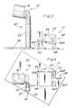
- FIG. 1 is an elevation of wafer inspection apparatus of the present invention shown as used in inspecting wafers for edge defects;
- FIG. 2 is an enlarged fragmentary view of the apparatus of Fig. 1;
- FIG. 3 is an elevation of the wafer inspection apparatus with the wafers, a wafer cassette, a wafer rotation device and a spacing member of the apparatus removed;
- FIG. 4 is a top plan of the apparatus;
- FIG. 5A is an elevation of a first spacing member of the apparatus;
- FIG. 5B is a bottom plan of the first spacing member;
- FIG. 6A is an elevation of a second spacing member of the apparatus; and
- FIG. 6B is a bottom plan of the second spacing member.
-
- Corresponding reference characters indicate corresponding parts throughout the several views of the drawings.
- Referring now to the drawings, and in particular to Fig. 1, apparatus for inspecting a plurality of semiconductor wafers is shown to include a support system, indicated generally at 10, supporting a
wafer cassette 12 holding the semiconductor wafers W. Thewafer cassette 12 is of conventional construction, having an open top, an open bottom and a series of partitions inside the cassette defining a plurality of parallel slots 14 (Fig. 2) for holding semiconductor wafers W of the same diameter. Eachwafer slot 14 is adapted to hold a single wafer W extending from the slot above the open top of thecassette 12. The wafers W are held by thecassette 12 in spaced apart parallel relation, each wafer having a center and a generally circular outer edge E. In fact, the wafers W are formed so that the edges each have a short segment (not shown) which is straight for purposes of orienting the wafers. However, the wafers W are generally circular. Thewafer cassette 12 holds the wafers W with their centers substantially on a common axis and their edges E substantially in alignment. - A light source, generally indicated at 16, is capable of projecting a well-defined columnar beam of light B (illustrated by parallel lines in Figs. 1 and 2) along a central longitudinal axis generally parallel to the common axis of the wafers W and generally tangential to the edges E of the wafers in the
cassette 12 to illuminate the edges. Thelight source 16 includes ahousing 18 which is mounted by a stand (generally indicated at 20) at a predetermined height. A projection lamp (not shown) having a brightness of about 21,000 foot candles (226042 lumens/m2) is located in the housing and provides the beam of light B. It has been found that a brightness of 18,000 foot candles (193750 lumens/m2) produces satisfactory results. However, it is to be understood that the brightness of the light may be lower than 18,000 foot candles (193750 lumens/m2) and still fall within the scope of the present invention. Thestand 20 includes a post 22 mounted on and projecting up from abase plate 24 of the apparatus, and a pivoting mount including avertical member 28 connected to the post and ahorizontal member 30 extending from the vertical member to thehousing 18. Thehorizontal member 30 is capable of pivoting about a horizontal axis relative to thevertical member 28 and post 22 to change the angle of the beam of light B so as to maintain the beam tangential to the upper portions of the edges E of the wafers W. Thehorizontal member 30 is capable of being fixed in a selected angular position by suitable locking devices, such as set screws (not shown). - The wafers W in the
wafer cassette 12 engage aroller 34 and the wafer cassette rests on aframe 36 of a wafer rotating device (indicated generally at 38) supported by thesupport system 10. Thewafer rotating device 38 is of a conventional construction, having anaxle 40 mounting theroller 34 which extends outwardly from theframe 36 to ahand grip 42. Wafer rotating devices of the same type aswafer rotating device 38 are used for orienting the wafers W in the cassette so that the straight portion of the edge E is at the bottom. Theroller 34 is located below the open bottom of thecassette 12 and its outer surface engages the edges E of the wafers in the cassette so that rotation of the roller causes the wafers W to rotate in an opposite direction within the wafer cassette. Thewafer cassette 12 is made of a suitable low-friction material (e.g., Teflon® or polypropylene) to minimize wear on the wafers W as they rotate in theirrespective slots 14. - Referring now to Figs. 3 and 4, the
support system 10 comprises a platform, indicated generally at 48, including a pair oflegs bolts 52 to thebase plate 24 and holding in cantilever fashion asupport plate 54 extending rearwardly and at a downward angle from the legs. Spaced rearwardly from the rear edge of thesupport plate 54 are a pair ofstandoffs base plate 24 bybolts 58. A forward facingsurface standoff support plate 54. Anupstanding side plate 62 attached bybolts 64 to theleg 50B and thestandoff 56B provides a guide surface against which thewafer cassette 12 may rest to be properly positioned. Aslot 66 in theside plate 62 facilitates placing thewafer cassette 12, thewafer rotating device 38 and other elements of the support system 10 (described hereinafter) on thesupport plate 54. - In a preferred embodiment, the
support system 10 further includes a riser generally indicated at 66 in Figs. 5A and 5B, comprising a pair of laterally spacedside members 66A, 66B and a top member 66C extending between and connecting the side members. Thesupport system 10 also includes a shorter riser, indicated generally at 68, which is shown in Figs. 6A-6B to comprise a pair of laterally spacedside members risers 66, 68 (broadly, "spacing members") permits the apparatus to be easily reconfigured in different modes for inspecting wafers of different diameters. In that regard, it may be seen that the difference between theriser 66 shown in Figs. 5A and 5B and theriser 68 shown in Figs. 6A and 6B is the height of their side members (66A, 66B and 68A, 68B). - The side members of the
risers tail 70 which is snugly received between the rear edge of thesupport plate 54 and the forwardly facingsurfaces standoffs side members 66A, 66B with thestandoffs riser 66 from sliding down thesloped support plate 54 on which it rests. Generally L-shapednotches 72 in the upper rear edges of theside members wafer rotating device 38 to be held in a flat position, parallel to the top member 66C, 68C of therisers support plate 54 of theplatform 48, or a portion of thewafer cassette 12. It is to be understood that thesupport system 10 of the present invention may include additional risers (not shown) or no risers, and still fall within the scope of the present invention. - Inspection of the wafers W using the apparatus of the present invention begins by determining whether one or
more risers light source 16. The determination will depend upon the diameter of the wafers W to be inspected. Assuming it is determined that theriser 66 is needed, it is placed on thesupport plate 54 of the platform and thewafer rotating device 38 is stacked upon the riser. It is to be understood that for large diameter wafers, no riser would be used and thewafer rotating device 38 would rest directly on thesupport plate 54 of the platform. - The
wafer cassette 12 will have been previously loaded with the polished surfaces of all the wafers W in the cassette facing in one direction and the unpolished surfaces facing in the other direction. Thewafer cassette 12 is placed on theriser 66 so that the polished surfaces face toward thelight source 16 and the unpolished surfaces face away from the light source. As supported on thewafer rotation device 38 andsupport system 10, thecassette 12 is tipped back so that the weight of the wafers W is largely supported by engagement of the unpolished surfaces of the wafers with the cassette in theslots 14. In this way, there is little opportunity for wear or other damage to the wafers W as they are rotated within thecassette 12. The portions of the edges E of the wafers located at the open bottom of thecassette 12 engage theroller 34 so that rotation of the roller by turning thehand grip 42 will cause the wafers W to rotate in an opposite direction. - The
light source 16 is energized so that the light beam B is projected generally tangentially to the edges E of the wafers W above thecassette 12. To more precisely align the beam of light B in tangential relation to the upper portions of the edges E, thehousing 18 of the light source may be pivoted relative to thevertical member 28 and post 22 by releasing and turning thehorizontal member 30 of thestand 20. As shown in Fig. 2, inspection of the edges E of the wafers is made visually from a position P above and forward of the location where the beam of light B is emitted from thehousing 18. It will be noted that portions of thevertical member 28 andhorizontal member 30 have been broken away in Fig. 2 to show the beam B continuously from thehousing 18 to the wafers W. By turning thehand grip 42, the inspector brings new portions of the edges E of the wafers into tangential relationship with the beam of light B. In this way, the inspector may inspect the entire circumference of all of the wafers W from a single vantage point with a simple manipulation of the apparatus. - The edges E of the wafers W which do not have a defect produce a diffused back scattering of the light in the beam B readily recognized by skilled inspectors. However, the presence of a defect in an edge E of one of the wafers W will cause a back scattering of light which can be observed by the inspector at position P as a point of light on the wafer edge. The back scattering of light from the beam B caused by a defect is diagrammatically illustrated by lines L in Fig. 2. The inspector may then remove the defective wafer or mark the wafer as having an edge defect. It has been found to be practical to inspect 25 wafers at a time for edge defects using the apparatus and method of the present invention. The limitation of 25 wafers arises only because the largest industry standard wafer carrier is sized to hold 25 wafers.
- Thus, it may be seen that the several objects and features of the present invention are achieved. Edge inspection of wafers W can be carried out rapidly because multiple wafers can be inspected at a single time by an inspector using the columnar beam of light from the
light source 16 directed tangentially to upper portions of the edges of the wafers. The wafers W can be held by the apparatus so that their weight is supported primarily on their unpolished surfaces, thereby protecting the polished surfaces. Moreover, the apparatus can includerisers - As various changes could be made in the above constructions without departing from the scope of the invention, it is intended that all matter contained in the above description or shown in the accompanying drawings shall be interpreted as illustrative and not in a limiting sense.
Claims (9)
- Apparatus for visually inspecting a plurality of semiconductor wafers in a single operation, said apparatus comprisinga holder (12) for holding a plurality of wafers (W) of substantially identical diameter in spaced apart parallel relation, each wafer having a center and a generally circular outer edge (E), said holder being adapted to hold the wafers with their centers substantially on a common axis,a light source (16) including a projection lamp for projecting a well-defined columnar beam (B) of light along a central longitudinal axis generally parallel to said common axis of the wafers and generally tangential to the edges of the wafers in the holder to thereby illuminate the edges (E), anda device (38) for rotating the wafers while the beam is projected on the edges of the wafers to enable visual detection of any imperfections in the edges of the wafers by detecting light back-scattered therefrom.
- Apparatus as set forth in claim 1, further comprising a housing (18) for said light source, a stand (20) for mounting the housing at a predetermined height, and means (30) for adjusting the angular position of the housing relative to the stand to change the direction of the light beam projected by the light source.
- Apparatus as set forth in claim 2, wherein said housing is mounted on the stand for pivotal movement about a generally horizontal axis.
- Apparatus as set forth in claim 1, wherein said holder comprises a cassette (12) having an open top, an open bottom and a series of partitions inside the cassette defining a plurality of parallel slots (14), each slot being adapted to hold a single wafer with the wafer extending from the slot above the open top of the cassette, and wherein said device for rotating the wafers comprises a roller (34) mounted below the open bottom of the cassette for rotation on an axis generally parallel to said common axis, said roller having an outer surface adapted for engagement with the edges of the wafers, and a mechanism for rotating the roller while the outer surface of the roller is in engagement with the wafers thereby to rotate the wafers about said common axis.
- Apparatus as set forth in any one of claims 1 to 4, further comprising a support system (10) for supporting said holder (12) so that the upper edges of the wafers held by the holder are generally tangential to said light beam projected by the light source.
- Apparatus as set forth in claim 5, wherein said light source is at a fixed height, said support system (10) comprising a support (48) and one or more devices (66, 68) cooperable with the support for supporting said holder at one or more different elevations to accommodate wafers of different diameters.
- Apparatus as set forth in claim 6, wherein each of said one or more devices cooperable with the support comprises a spacing member adapted to be placed on the support below the holder.
- A method of inspecting a plurality of semiconductor wafers in a single operation, each wafer having a center and a generally circular outer edge, said method comprising the following steps:holding a plurality of generally round semiconductor wafers of substantially identical diameter so that the wafers are spaced apart and generally parallel with respect to one another with the centers of the wafers substantially on a common axis,projecting a well-defined columnar beam (B) of light from a projection lamp along a central longitudinal axis generally parallel to said common axis of the wafers and generally tangential to the edges of said plurality of wafers thereby to illuminate the edges (E),rotating the wafers while the beam is projected on the edges of the wafers, andvisually detecting any imperfections in the edges of the wafers as the wafers rotate by visual observation from a location above and near the light source, and wherein said visual observation involves observing back scattering of the beam of light for indications of imperfections in a wafer.
- A method as set forth in claim 8, further comprising holding the wafers so that the common axis of the wafers is at a fixed angle, and adjusting the angle of the light beam so that it is parallel to said fixed angle.
Applications Claiming Priority (2)
| Application Number | Priority Date | Filing Date | Title |
|---|---|---|---|
| US436840 | 1995-05-08 | ||
| US08/436,840 US5592295A (en) | 1995-05-08 | 1995-05-08 | Apparatus and method for semiconductor wafer edge inspection |
Publications (3)
| Publication Number | Publication Date |
|---|---|
| EP0742587A2 EP0742587A2 (en) | 1996-11-13 |
| EP0742587A3 EP0742587A3 (en) | 1997-06-11 |
| EP0742587B1 true EP0742587B1 (en) | 2000-07-19 |
Family
ID=23734030
Family Applications (1)
| Application Number | Title | Priority Date | Filing Date |
|---|---|---|---|
| EP96302674A Expired - Lifetime EP0742587B1 (en) | 1995-05-08 | 1996-04-17 | Apparatus and method for semiconductor wafer edge inspection |
Country Status (9)
| Country | Link |
|---|---|
| US (1) | US5592295A (en) |
| EP (1) | EP0742587B1 (en) |
| JP (1) | JPH08340031A (en) |
| KR (1) | KR100261832B1 (en) |
| CN (1) | CN1142685A (en) |
| DE (1) | DE69609377T2 (en) |
| MY (1) | MY113745A (en) |
| SG (1) | SG49948A1 (en) |
| TW (1) | TW344111B (en) |
Families Citing this family (34)
| Publication number | Priority date | Publication date | Assignee | Title |
|---|---|---|---|---|
| KR100278807B1 (en) * | 1998-05-01 | 2001-01-15 | 신덕교 | Wafer inspection system |
| WO2000002236A2 (en) | 1998-07-07 | 2000-01-13 | Memc Electronic Materials, Inc. | Radio frequency identification system and method for tracking silicon wafers |
| US6535628B2 (en) | 1998-10-15 | 2003-03-18 | Applied Materials, Inc. | Detection of wafer fragments in a wafer processing apparatus |
| EP1001460B1 (en) * | 1998-10-15 | 2001-05-02 | Wacker Siltronic Gesellschaft für Halbleitermaterialien Aktiengesellschaft | Method and apparatus for detecting, monitoring and characterizing edge defects on semiconductor wafers |
| US6062084A (en) * | 1999-01-29 | 2000-05-16 | Taiwan Semiconductor Manufacturing Co., Ltd. | Apparatus for detecting wafer edge defects and method of using |
| US6306670B1 (en) * | 1999-08-12 | 2001-10-23 | Lucent Technologies Inc. | Tool for handling a workpiece |
| US6566673B1 (en) | 2000-07-07 | 2003-05-20 | Daitron Inc. | Method and apparatus for detecting defects along the edge of electronic media |
| US6545752B1 (en) | 2000-07-07 | 2003-04-08 | Daitron, Inc. | Method and apparatus for detecting defects along the edge of electronic media |
| KR100403862B1 (en) * | 2001-01-26 | 2003-11-01 | 어플라이드비전텍(주) | Apparatus for inspecting semiconductor wafer and the methods thereof |
| US6865948B1 (en) * | 2002-01-29 | 2005-03-15 | Taiwan Semiconductor Manufacturing Company | Method of wafer edge damage inspection |
| JP3629244B2 (en) * | 2002-02-19 | 2005-03-16 | 本多エレクトロン株式会社 | Wafer inspection equipment |
| US6785009B1 (en) * | 2002-02-28 | 2004-08-31 | Advanced Micro Devices, Inc. | Method of using high yielding spectra scatterometry measurements to control semiconductor manufacturing processes, and systems for accomplishing same |
| KR100460807B1 (en) * | 2002-07-08 | 2004-12-09 | 삼성전자주식회사 | wafer shape inspection equipment of semiconductor devise manufacturing equipment, cleaning equipment the using and inspection method there of |
| US7204669B2 (en) * | 2002-07-17 | 2007-04-17 | Applied Materials, Inc. | Semiconductor substrate damage protection system |
| CN100529743C (en) * | 2003-05-19 | 2009-08-19 | 微-埃普西龙测量技术有限两合公司 | Method and apparatus for optically controlling the quality of a preferably rounded-edged article |
| US7220034B2 (en) * | 2003-07-11 | 2007-05-22 | Rudolph Technologies, Inc. | Fiber optic darkfield ring light |
| WO2005008735A2 (en) * | 2003-07-14 | 2005-01-27 | August Technology Corporation | Photoresist edge bead removal measurement |
| US6947588B2 (en) * | 2003-07-14 | 2005-09-20 | August Technology Corp. | Edge normal process |
| US7340087B2 (en) * | 2003-07-14 | 2008-03-04 | Rudolph Technologies, Inc. | Edge inspection |
| US7316938B2 (en) * | 2003-07-14 | 2008-01-08 | Rudolph Technologies, Inc. | Adjustable film frame aligner |
| US20050052197A1 (en) * | 2003-07-14 | 2005-03-10 | Cory Watkins | Multi-tool manager |
| US8698327B2 (en) | 2003-07-14 | 2014-04-15 | Rudolph Technologies, Inc. | Substrate handler |
| US7589783B2 (en) * | 2003-07-14 | 2009-09-15 | Rudolph Technologies, Inc. | Camera and illumination matching for inspection system |
| US8045788B2 (en) * | 2003-07-14 | 2011-10-25 | August Technology Corp. | Product setup sharing for multiple inspection systems |
| US7280200B2 (en) * | 2003-07-18 | 2007-10-09 | Ade Corporation | Detection of a wafer edge using collimated light |
| US6934661B2 (en) * | 2003-12-16 | 2005-08-23 | Taiwan Semiconductor Manufacturing Co., Ltd. | Wafer edge detector |
| TWI512865B (en) | 2008-09-08 | 2015-12-11 | Rudolph Technologies Inc | Wafer edge inspection |
| US9658169B2 (en) | 2013-03-15 | 2017-05-23 | Rudolph Technologies, Inc. | System and method of characterizing micro-fabrication processes |
| JP6229438B2 (en) * | 2013-11-01 | 2017-11-15 | 株式会社Sumco | Inspection device and inspection method for outer periphery of semiconductor wafer |
| US9348057B2 (en) | 2014-07-24 | 2016-05-24 | International Business Machines Corporation | Method and apparatus for calibrating sensors that detect wafer protrusion from a wafer cassette |
| KR101984386B1 (en) * | 2017-07-13 | 2019-05-30 | 에스케이실트론 주식회사 | Visual inspection apparatus of wafer cleaning equipment |
| CN108519390B (en) * | 2018-04-09 | 2021-02-02 | 芜湖立普德机械科技有限公司 | Glass substrate detection device |
| CN112570306B (en) * | 2020-11-13 | 2025-07-29 | 马达西奇(苏州)智能装备科技有限公司 | Wafer inspection and cleaning equipment |
| CN112665536A (en) * | 2020-12-30 | 2021-04-16 | 上海新昇半导体科技有限公司 | Method and device for measuring edge roughness of wafer |
Family Cites Families (7)
| Publication number | Priority date | Publication date | Assignee | Title |
|---|---|---|---|---|
| US4954721A (en) * | 1988-03-30 | 1990-09-04 | Tel Sagami Limited | Apparatus for detecting an array of wafers |
| US5003188A (en) * | 1988-11-18 | 1991-03-26 | Tokyo Aircraft Instrument Co., Ltd. | Semiconductor waxer detection system |
| JP2674874B2 (en) * | 1990-11-13 | 1997-11-12 | 九州日本電気株式会社 | Semiconductor manufacturing equipment |
| JPH04177851A (en) * | 1990-11-13 | 1992-06-25 | Nec Kyushu Ltd | Device for inspecting wafer appearance |
| JP2876507B2 (en) * | 1993-04-14 | 1999-03-31 | 日立電子エンジニアリング株式会社 | Wafer foreign matter inspection device |
| JP2798112B2 (en) * | 1994-03-25 | 1998-09-17 | 信越半導体株式会社 | Apparatus and method for measuring wafer notch size |
| US5504345A (en) * | 1994-04-14 | 1996-04-02 | Hama Laboratories, Inc. | Dual beam sensor and edge detection system and method |
-
1995
- 1995-05-08 US US08/436,840 patent/US5592295A/en not_active Expired - Fee Related
- 1995-12-28 TW TW084114060A patent/TW344111B/en active
-
1996
- 1996-04-17 EP EP96302674A patent/EP0742587B1/en not_active Expired - Lifetime
- 1996-04-17 DE DE69609377T patent/DE69609377T2/en not_active Expired - Fee Related
- 1996-04-26 MY MYPI96001605A patent/MY113745A/en unknown
- 1996-05-01 JP JP8110795A patent/JPH08340031A/en not_active Withdrawn
- 1996-05-07 SG SG1996009747A patent/SG49948A1/en unknown
- 1996-05-07 CN CN96106205A patent/CN1142685A/en active Pending
- 1996-05-07 KR KR1019960014902A patent/KR100261832B1/en not_active Expired - Fee Related
Also Published As
| Publication number | Publication date |
|---|---|
| KR100261832B1 (en) | 2000-07-15 |
| DE69609377D1 (en) | 2000-08-24 |
| KR960043072A (en) | 1996-12-23 |
| MY113745A (en) | 2002-05-31 |
| CN1142685A (en) | 1997-02-12 |
| JPH08340031A (en) | 1996-12-24 |
| DE69609377T2 (en) | 2000-12-07 |
| EP0742587A3 (en) | 1997-06-11 |
| EP0742587A2 (en) | 1996-11-13 |
| TW344111B (en) | 1998-11-01 |
| US5592295A (en) | 1997-01-07 |
| SG49948A1 (en) | 1998-06-15 |
Similar Documents
| Publication | Publication Date | Title |
|---|---|---|
| US5592295A (en) | Apparatus and method for semiconductor wafer edge inspection | |
| US6559938B1 (en) | Backside contamination inspection device | |
| US5959461A (en) | Probe station adapter for backside emission inspection | |
| FR2666413A1 (en) | SYSTEM AND METHOD FOR VISUAL EXAMINATION OF PHARMACEUTICAL TABLETS. | |
| KR101980860B1 (en) | A spring pin separating apparatus | |
| US6062084A (en) | Apparatus for detecting wafer edge defects and method of using | |
| KR102136084B1 (en) | System for inspecting edge area of wafer | |
| EP0730147B1 (en) | Apparatus for inspecting O-rings | |
| KR20190134275A (en) | System for inspecting edge area of wafer and method using the same | |
| CN115088060A (en) | Wafer edge defect inspection device and inspection method | |
| CN1109973A (en) | Inspection of translucent containers | |
| JP7569541B2 (en) | Visual Inspection Equipment | |
| CN117739872A (en) | Detection device for flatness of graphite piece | |
| CN109443280A (en) | A kind of lens detection device | |
| JP3009659B1 (en) | Light source for flaw inspection and light source unit for flaw inspection | |
| JP2001041720A (en) | Defect detection method and apparatus | |
| US20020075478A1 (en) | Inspection device having wafer exchange stage | |
| JP2535514B2 (en) | Method of attaching probe card and wafer prober equipped with the same | |
| JP2004514132A (en) | Apparatus and method for optically measuring small grains, such as cereal grains, such as grains | |
| EP0100446A1 (en) | High resolution electronic automatic imaging and inspecting system | |
| JP2000111484A (en) | Inspection apparatus for defect of wafer | |
| JP2001007188A (en) | Suction mounting table and foreign matter inspection device using the same | |
| JPH0755711A (en) | Semiconductor device inspection equipment | |
| JPS58108442A (en) | Inspecting device for bottle | |
| JPH03264851A (en) | Method and apparatus for inspecting defect in edge of plate material |
Legal Events
| Date | Code | Title | Description |
|---|---|---|---|
| PUAI | Public reference made under article 153(3) epc to a published international application that has entered the european phase |
Free format text: ORIGINAL CODE: 0009012 |
|
| AK | Designated contracting states |
Kind code of ref document: A2 Designated state(s): DE FR GB IT |
|
| PUAL | Search report despatched |
Free format text: ORIGINAL CODE: 0009013 |
|
| AK | Designated contracting states |
Kind code of ref document: A3 Designated state(s): DE FR GB IT |
|
| 17P | Request for examination filed |
Effective date: 19971031 |
|
| 17Q | First examination report despatched |
Effective date: 19980518 |
|
| GRAG | Despatch of communication of intention to grant |
Free format text: ORIGINAL CODE: EPIDOS AGRA |
|
| GRAG | Despatch of communication of intention to grant |
Free format text: ORIGINAL CODE: EPIDOS AGRA |
|
| GRAH | Despatch of communication of intention to grant a patent |
Free format text: ORIGINAL CODE: EPIDOS IGRA |
|
| GRAH | Despatch of communication of intention to grant a patent |
Free format text: ORIGINAL CODE: EPIDOS IGRA |
|
| GRAA | (expected) grant |
Free format text: ORIGINAL CODE: 0009210 |
|
| AK | Designated contracting states |
Kind code of ref document: B1 Designated state(s): DE FR GB IT |
|
| REF | Corresponds to: |
Ref document number: 69609377 Country of ref document: DE Date of ref document: 20000824 |
|
| ITF | It: translation for a ep patent filed | ||
| ET | Fr: translation filed | ||
| PGFP | Annual fee paid to national office [announced via postgrant information from national office to epo] |
Ref country code: FR Payment date: 20010409 Year of fee payment: 6 Ref country code: DE Payment date: 20010409 Year of fee payment: 6 |
|
| PGFP | Annual fee paid to national office [announced via postgrant information from national office to epo] |
Ref country code: GB Payment date: 20010411 Year of fee payment: 6 |
|
| PLBE | No opposition filed within time limit |
Free format text: ORIGINAL CODE: 0009261 |
|
| STAA | Information on the status of an ep patent application or granted ep patent |
Free format text: STATUS: NO OPPOSITION FILED WITHIN TIME LIMIT |
|
| 26N | No opposition filed | ||
| REG | Reference to a national code |
Ref country code: GB Ref legal event code: IF02 |
|
| PG25 | Lapsed in a contracting state [announced via postgrant information from national office to epo] |
Ref country code: GB Free format text: LAPSE BECAUSE OF NON-PAYMENT OF DUE FEES Effective date: 20020417 |
|
| PG25 | Lapsed in a contracting state [announced via postgrant information from national office to epo] |
Ref country code: DE Free format text: LAPSE BECAUSE OF NON-PAYMENT OF DUE FEES Effective date: 20021101 |
|
| GBPC | Gb: european patent ceased through non-payment of renewal fee |
Effective date: 20020417 |
|
| PG25 | Lapsed in a contracting state [announced via postgrant information from national office to epo] |
Ref country code: FR Free format text: LAPSE BECAUSE OF NON-PAYMENT OF DUE FEES Effective date: 20021231 |
|
| REG | Reference to a national code |
Ref country code: FR Ref legal event code: ST |
|
| PG25 | Lapsed in a contracting state [announced via postgrant information from national office to epo] |
Ref country code: IT Free format text: LAPSE BECAUSE OF NON-PAYMENT OF DUE FEES;WARNING: LAPSES OF ITALIAN PATENTS WITH EFFECTIVE DATE BEFORE 2007 MAY HAVE OCCURRED AT ANY TIME BEFORE 2007. THE CORRECT EFFECTIVE DATE MAY BE DIFFERENT FROM THE ONE RECORDED. Effective date: 20050417 |