EP0740425A1 - Precision digital-to-analogue converter - Google Patents
Precision digital-to-analogue converter Download PDFInfo
- Publication number
- EP0740425A1 EP0740425A1 EP96410037A EP96410037A EP0740425A1 EP 0740425 A1 EP0740425 A1 EP 0740425A1 EP 96410037 A EP96410037 A EP 96410037A EP 96410037 A EP96410037 A EP 96410037A EP 0740425 A1 EP0740425 A1 EP 0740425A1
- Authority
- EP
- European Patent Office
- Prior art keywords
- transistors
- voltage
- transistor
- vout
- current
- Prior art date
- Legal status (The legal status is an assumption and is not a legal conclusion. Google has not performed a legal analysis and makes no representation as to the accuracy of the status listed.)
- Granted
Links
Images

Classifications
-
- H—ELECTRICITY
- H03—ELECTRONIC CIRCUITRY
- H03M—CODING; DECODING; CODE CONVERSION IN GENERAL
- H03M1/00—Analogue/digital conversion; Digital/analogue conversion
- H03M1/66—Digital/analogue converters
- H03M1/74—Simultaneous conversion
- H03M1/742—Simultaneous conversion using current sources as quantisation value generators
- H03M1/745—Simultaneous conversion using current sources as quantisation value generators with weighted currents
Definitions
- the present invention relates to precision digital / analog converters, such as those used in the reproduction of the sound recorded on laser discs.
- a battery of current sources is commonly used which are connected in greater or lesser number on a common output line as a function of digital data. Given the inevitable pairing faults between the current sources, the precision obtained by this method cannot exceed 10 bits.
- FIG. 1 schematically illustrates a digital / analog converter making it possible to obtain a higher precision, described in an article of IEEE Journal of Solid-State Circuits, vol. 16, No. 12, December 1991, entitled "An Oversampled Multibit CMOS D / A Converter for Digital Audio with 115-dB Dynamic Range".
- This converter includes a battery of positive current sources IP1 to IPn and a battery of negative current sources IN1 to INn.
- a digital control signal C selects the positive or negative current sources to be connected in a complementary manner to two differential output lines Iout and Iout *. Operating in differential mode improves certain characteristics, such as noise sensitivity.
- the current sources IP and IN have the same value I, and they are generally switched so that they are always connected to one or the other of the lines Iout and Iout *, to avoid switching noise.
- each IP source is periodically calibrated to an IPc calibration source, and each IN source is periodically calibrated to an INc calibration source.
- the value of an IP or IN source is kept between two calibrations by capacitive effect. It is thus ensured that the value of each of the IP sources is equal to the value of the calibration source IPc and that the value of each of the sources IN is equal to the value of the calibration source INc.
- the lines Iout and Iout * vary symmetrically with respect to each other.
- the value of the IN sources must be equal to the value of the IP sources, or that the value of the IPc calibration source is equal to the value of the INc calibration source.
- the batteries of IP and IN sources each include an additional source, respectively IPs and INs connected to each other.
- the current difference between the sources IPs and INs is taken by an integrator 10, the output of which readjusts the value of the calibration source INc until the currents of the sources IPs and INs are equal.
- the quality of this symmetry setting depends on the pairing of the IPs source with each of the IP sources and on the pairing of the INs source with each of the IN sources. Given the large number of sources, matching is particularly difficult.
- An object of the present invention is to provide a precision digital / analog converter in which the adjustment of the symmetry is particularly precise.
- a digital / analog converter comprising pairs of positive and negative current sources connected by switches with two differential output lines, the switches being controlled as a function of digital data.
- Each pair of current sources is a pair of transistors of an output stage of a transconductance amplifier receiving a reference voltage on a non-inverting input and, on its inverting input, the voltage at the midpoint of a bridge. of resistors connected between the differential lines, the converter output being the voltage between the two differential lines.
- the transconductance amplifier comprises a differential stage, the current in a first branch of this differential stage being copied into first transistors of the pairs of transistors and the current of a second branch of l 'differential stage being copied into the second transistors of the pairs of transistors.
- the transistors of the couples of the transistors are connected to respective cascode transistors, polarized with respect to the voltage at the midpoint of the resistance bridge.
- a battery of positive current sources is constituted by P channel MP MP MOS transistors connected in parallel by their sources and their gates, the sources being connected to a high supply voltage Vcc.
- a complementary battery of negative current sources is constituted by N-channel MOS transistors MN connected in parallel by their sources and their gates, the sources being connected to a low supply potential GND.
- the drain of each of the transistors MP is connected to two differential output lines Vout and Vout * by two respective switches KP and KP *.
- the drain of each of the transistors MN is connected to the lines Vout and Vout * by two respective switches KN and KN *.
- the transistors MP and MN form an output stage of a transconductance amplifier.
- This amplifier comprises a differential input stage 12 formed, for example, of two P-channel MOS transistors MP1 and MP2, the sources of which are connected to the potential Vcc by a source of quiescent current 14.
- the drain current of the transistor MP1, forming a first branch of stage 12 is copied into each of the transistors MP by a first current mirror circuit.
- the drain current of the transistor MP2, forming a second branch of the stage 12 is copied into each of the transistors MN by a second current mirror circuit.
- the first current mirror circuit comprises an N-channel MOS transistor MN3 whose drain and gate are connected to the drain of transistor MP1, and whose source is connected GND potential.
- An N-channel MOS transistor MN4 is connected in parallel to the transistor MN3 by its gate and its source and forms with the transistor MN3 a current mirror which copies the current from the transistor MP1 into the transistor MN4.
- the drain of this transistor MN4 is connected to the drain and to the gate of a P-channel MOS transistor MP5 whose source is connected to the potential Vcc.
- this transistor MP5 is connected in parallel by its gate and its source on the transistors MP.
- the transistors MP5 and MP form a current mirror which copies in each of the transistors MP the drain current of the transistor MN4, and therefore of the transistor MP1.
- the second current mirror circuit comprises an N-channel MOS transistor MN6, the drain and the gate of which are connected to the drain of the transistor MP2.
- this transistor MN6 is connected in parallel by its gate and its source to the transistors MN and forms with these a current mirror which copies in each of the transistors MN the drain current of the transistor MP2.
- the gate of transistor MP1 constitutes an inverting input of the transconductance amplifier, and the gate of transistor MP2 constitutes a non-inverting input.
- the gate of the transistor MP1 receives the voltage Vc present at the midpoint of a resistor bridge R of the same value connected between the differential output lines Vout and Vout *.
- the output of the converter according to the invention is the differential voltage present at the terminals of the resistance bridge R (or between the lines Vout and Vout *).
- the gate of the transistor MP2 receives a reference voltage Vr, which is the voltage with respect to which the output of the converter must be symmetrical.
- the voltage Vc is regulated on the voltage of reference Vr, which ensures the symmetry of the voltage between the lines Vout and Vout * with respect to the voltage Vr, regardless of the number of MP or MN sources connected to the lines Vout and Vout *, provided that at least one MP source is connected to one of the lines Vout and Vout * and at least one source MN to the other of the lines.
- the current of the transistor MP1 decreases.
- the conductance of the transistors MP decreases, which causes the voltage Vc to decrease.
- the current of the transistor MP2 increases symmetrically with the decrease of the current of the transistor MP1.
- the conductance of the transistors MN increases, which also tends to decrease the voltage Vc.
- this circuit effectively tends to restore the equilibrium point where the voltage Vc is equal to the reference voltage Vr.
- the symmetry of the output signal that is to say the differential voltage between the lines Vout and Vout *, depends only on the ratio of the resistors R. The pairing of only two resistors can be carried out in a particularly precise way, since the resistors R can be integrated very close to each other.
- a converter according to the invention is particularly well suited to a particular method of switching the MP and MN transistors making it possible to obtain the desired precision, this method being notably simpler to implement and as precise as the self-calibration method. described in relation to Figure 1.
- This is a so-called "butterfly" switching method.
- this method consists in choosing, at each switching, a pseudo-random combination of m transistors MP and m transistors MN among the set of transistors that one can choose.
- the best results are obtained if these switching operations are carried out at a frequency clearly greater than the sampling frequency of the digital data to be converted.
- FIG. 3 represents a modification of the converter of FIG. 2, intended to make the converter less sensitive to variations in its supply voltage.
- Each of the transistors MP is connected to its switches KP and KP * via a cascode transistor with P channel MPc.
- each of the transistors MN is connected to its switches KN and KN * via an N-channel cascode transistor MNc.
- the amplifier includes an additional output stage intended to polarize the cascode transistors MPc and MNc. This additional stage comprises a P-channel MOS transistor MP7 connected in parallel by its gate and its source on the MP transistors and an N-channel MOS transistor MN7 connected in parallel by its gate and its source on the MN transistors.
- the drain of the transistor MP7 is connected to the midpoint of the resistance bridge R by a P-channel MOS transistor MP8, the drain and the gate of which are connected to the gates of the transistors MPc.
- the transistor MN7 is connected to the midpoint of the resistance bridge R by an N-channel MOS transistor MN8, the drain and the gate of which are connected to the gates of the transistors MNc.
- the drain potential of the transistors MP is fixed at the potential Vc increased by the threshold voltage of the transistors MPc, and the drain potential of the transistors MN is fixed at the potential Vc reduced by the threshold voltage of the transistors MNc.
- the peak voltage on the output Vout or Vout * is thus limited to the threshold voltage of a transistor MPc or MNc, which is sufficient.
- the additional output stage comprising the transistors MP7 and MN7 operates under the same conditions as the output stage formed by the transistors MP and MN, and does not inject in principle no current in the resistors R. However, if there is a symmetry defect on the output stage comprising the transistors MP and MN, the additional stage absorbs a residual current through the resistors R, which contributes to compensate for the lack of symmetry.
- An additional N-channel cascode transistor MN9 is disposed between the transistors MN4 and MP5 and its gate is connected to the gates of the transistors MNc.
- This cascode transistor makes it possible to operate the current mirror MN3 / MN4 under the same conditions as the current mirror MN6 / MN, which contributes to improving the symmetry.
Abstract
Description
La présente invention concerne les convertisseurs numérique/analogique de précision, tels que ceux utilisés dans la restitution du son enregistré sur les disques laser.The present invention relates to precision digital / analog converters, such as those used in the reproduction of the sound recorded on laser discs.
Pour effectuer une conversion numérique/analogique avec une précision moyenne, on utilise couramment une batterie de sources de courant qui sont connectées en plus ou moins grand nombre sur une ligne de sortie commune en fonction d'une donnée numérique. Etant donné les défauts d'appariement inévitables entre les sources de courant, la précision obtenue par cette méthode ne peut dépasser 10 bits.To carry out a digital / analog conversion with average precision, a battery of current sources is commonly used which are connected in greater or lesser number on a common output line as a function of digital data. Given the inevitable pairing faults between the current sources, the precision obtained by this method cannot exceed 10 bits.
La figure 1 illustre schématiquement un convertisseur numérique/analogique permettant d'obtenir une précision plus élevée, décrit dans un article de IEEE Journal of Solid-State Circuits, vol. 16, N° 12, décembre 1991, intitulé "An Oversampled Multibit CMOS D/A Converter for Digital Audio with 115-dB Dynamic Range". Ce convertisseur comprend une batterie de sources de courant positives IP1 à IPn et une batterie de sources de courant négatives IN1 à INn. Un signal de commande numérique C sélectionne les sources de courant positives ou négatives à connecter de façon complémentaire à deux lignes de sortie différentielles Iout et Iout*. Le fonctionnement en mode différentiel permet d'améliorer certaines caractéristiques, telles que la sensibilité au bruit. Les sources de courant IP et IN sont de même valeur I, et elles sont généralement commutées de manière qu'elles soient toujours connectées à l'une ou l'autre des lignes Iout et Iout*, pour éviter du bruit de commutation.FIG. 1 schematically illustrates a digital / analog converter making it possible to obtain a higher precision, described in an article of IEEE Journal of Solid-State Circuits, vol. 16, No. 12, December 1991, entitled "An Oversampled Multibit CMOS D / A Converter for Digital Audio with 115-dB Dynamic Range". This converter includes a battery of positive current sources IP1 to IPn and a battery of negative current sources IN1 to INn. A digital control signal C selects the positive or negative current sources to be connected in a complementary manner to two differential output lines Iout and Iout *. Operating in differential mode improves certain characteristics, such as noise sensitivity. The current sources IP and IN have the same value I, and they are generally switched so that they are always connected to one or the other of the lines Iout and Iout *, to avoid switching noise.
Pour obtenir une grande précision de la conversion, chaque source IP est périodiquement étalonnée sur une source d'étalonnage IPc, et chaque source IN est périodiquement étalonnée sur une source d'étalonnage INc. La valeur d'une source IP ou IN est conservée entre deux étalonnages par effet capacitif. On assure ainsi que la valeur de chacune des sources IP est égale à la valeur de la source d'étalonnage IPc et que la valeur de chacune des sources IN est égale à la valeur de la source d'étalonnage INc.To obtain high conversion accuracy, each IP source is periodically calibrated to an IPc calibration source, and each IN source is periodically calibrated to an INc calibration source. The value of an IP or IN source is kept between two calibrations by capacitive effect. It is thus ensured that the value of each of the IP sources is equal to the value of the calibration source IPc and that the value of each of the sources IN is equal to the value of the calibration source INc.
Pour réduire la distorsion, il est nécessaire que les lignes Iout et Iout* varient de manière symétrique l'une par rapport à l'autre. Ceci entraîne que la valeur des sources IN doit être égale à la valeur des sources IP, ou encore que la valeur de la source d'étalonnage IPc soit égale à la valeur de la source d'étalonnage INc. Pour cela, les batteries de sources IP et IN comprennent chacune une source supplémentaire, respectivement IPs et INs reliées l'une à l'autre. La différence de courant entre les sources IPs et INs est prélevée par un intégrateur 10 dont la sortie réajuste la valeur de la source d'étalonnage INc jusqu'à ce que les courants des sources IPs et INs soient égaux.To reduce the distortion, it is necessary that the lines Iout and Iout * vary symmetrically with respect to each other. This means that the value of the IN sources must be equal to the value of the IP sources, or that the value of the IPc calibration source is equal to the value of the INc calibration source. For this, the batteries of IP and IN sources each include an additional source, respectively IPs and INs connected to each other. The current difference between the sources IPs and INs is taken by an
Toutefois, la qualité de ce réglage de symétrie dépend de l'appariement de la source IPs avec chacune des sources IP et de l'appariement de la source INs avec chacune des sources IN. Etant donné le nombre important de sources, l'appariement est particulièrement difficile.However, the quality of this symmetry setting depends on the pairing of the IPs source with each of the IP sources and on the pairing of the INs source with each of the IN sources. Given the large number of sources, matching is particularly difficult.
Un objet de la présente invention est de prévoir un convertisseur numérique/analogique de précision dans lequel le réglage de la symétrie est particulièrement précis.An object of the present invention is to provide a precision digital / analog converter in which the adjustment of the symmetry is particularly precise.
Cet objet est atteint grâce à un convertiseur numérique/analogique comprenant des couples de sources de courant positives et négatives reliées par des interrupteurs à deux lignes de sortie différentielles, les interrupteurs étant commandés en fonction d'une donnée numérique. Chaque couple de sources de courant est un couple de transistors d'un étage de sortie d'un amplificateur à transconductance recevant une tension de référence sur une entrée non-inverseuse et, sur son entrée inverseuse, la tension au point milieu d'un pont de résistances connecté entre les lignes différentielles, la sortie du convertisseur étant la tension entre les deux lignes différentielles.This object is achieved thanks to a digital / analog converter comprising pairs of positive and negative current sources connected by switches with two differential output lines, the switches being controlled as a function of digital data. Each pair of current sources is a pair of transistors of an output stage of a transconductance amplifier receiving a reference voltage on a non-inverting input and, on its inverting input, the voltage at the midpoint of a bridge. of resistors connected between the differential lines, the converter output being the voltage between the two differential lines.
Selon un mode de réalisation de la présente invention, l'amplificateur à transconductance comprend un étage différentiel, le courant dans une première branche de cet étage différentiel étant recopié dans des premiers transistors des couples de transistors et le courant d'une deuxième branche de l'étage différentiel étant recopié dans les deuxièmes transistors des couples de transistors.According to one embodiment of the present invention, the transconductance amplifier comprises a differential stage, the current in a first branch of this differential stage being copied into first transistors of the pairs of transistors and the current of a second branch of l 'differential stage being copied into the second transistors of the pairs of transistors.
Selon un mode de réalisation de la présente invention, les transistors des couples des transistors sont reliés à des transistors cascode respectifs, polarisés par rapport à la tension au point milieu du pont de résistances.According to an embodiment of the present invention, the transistors of the couples of the transistors are connected to respective cascode transistors, polarized with respect to the voltage at the midpoint of the resistance bridge.
Ces objets, caractéristiques et avantages ainsi que d'autres de la présente invention seront exposés en détail dans la description suivante de modes de réalisation particuliers, faite à titre non-limitatif à l'aide des figures jointes, parmi lesquelles :
- la figure 1, précédemment décrite, représente schématiquement un convertisseur numérique/analogique de précision classique ;
- la figure 2 représente un mode de réalisation de convertisseur numérique/analogique selon l'invention ; et
- la figure 3 représente un autre mode de réalisation de convertisseur numérique/analogique selon l'invention.
- FIG. 1, previously described, schematically represents a conventional precision digital / analog converter;
- FIG. 2 represents an embodiment of digital / analog converter according to the invention; and
- FIG. 3 represents another embodiment of a digital / analog converter according to the invention.
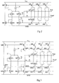
A la figure 2, une batterie de sources de courant positives est constituée par des transistors MOS à canal P MP reliés en parallèle par leurs sources et leurs grilles, les sources étant reliées à un potentiel d'alimentation haut Vcc. Une batterie complémentaire de sources de courant négatives est constituée par des transistors MOS à canal N MN reliés en parallèle par leurs sources et leurs grilles, les sources étant reliées à un potentiel d'alimentation bas GND. Le drain de chacun des transistors MP est relié à deux lignes de sortie différentielles Vout et Vout* par deux interrupteurs respectifs KP et KP*. Le drain de chacun des transistors MN est relié aux lignes Vout et Vout* par deux interrupteurs respectifs KN et KN*. Ces interrupteurs KP, KN, KP* et KN* peuvent être commandés de manière classique à partir d'une donnée numérique afin d'établir un signal différentiel analogique correspondant sur les lignes Vout et Vout*.In FIG. 2, a battery of positive current sources is constituted by P channel MP MP MOS transistors connected in parallel by their sources and their gates, the sources being connected to a high supply voltage Vcc. A complementary battery of negative current sources is constituted by N-channel MOS transistors MN connected in parallel by their sources and their gates, the sources being connected to a low supply potential GND. The drain of each of the transistors MP is connected to two differential output lines Vout and Vout * by two respective switches KP and KP *. The drain of each of the transistors MN is connected to the lines Vout and Vout * by two respective switches KN and KN *. These switches KP, KN, KP * and KN * can be conventionally controlled from digital data in order to establish a corresponding analog differential signal on the Vout and Vout * lines.
Selon l'invention, les transistors MP et MN forment un étage de sortie d'un amplificateur à transconductance. Cet amplificateur comprend un étage différentiel d'entrée 12 formé, par exemple, de deux transistors MOS à canal P MP1 et MP2 dont les sources sont reliées au potentiel Vcc par une source de courant de repos 14. Le courant de drain du transistor MP1, formant une première branche de l'étage 12, est recopié dans chacun des transistors MP par un premier circuit à miroir de courant. De même, le courant de drain du transistor MP2, formant une deuxième branche de l'étage 12, est recopié dans chacun des transistors MN par un deuxième circuit à miroir de courant.According to the invention, the transistors MP and MN form an output stage of a transconductance amplifier. This amplifier comprises a
Le premier circuit à miroir de courant comprend un transistor MOS à canal N MN3 dont le drain et la grille sont reliés au drain du transistor MP1, et dont la source est reliée au potentiel GND. Un transistor MOS à canal N MN4 est relié en parallèle sur le transistor MN3 par sa grille et sa source et forme avec le transistor MN3 un miroir de courant qui recopie le courant du transistor MP1 dans le transistor MN4. Le drain de ce transistor MN4 est relié au drain et à la grille d'un transistor MOS à canal P MP5 dont la source est reliée au potentiel Vcc. En outre, ce transistor MP5 est relié en parallèle par sa grille et sa source sur les transistors MP. Ainsi, les transistors MP5 et MP forment un miroir de courant qui recopie dans chacun des transistors MP le courant de drain du transistor MN4, et donc du transistor MP1.The first current mirror circuit comprises an N-channel MOS transistor MN3 whose drain and gate are connected to the drain of transistor MP1, and whose source is connected GND potential. An N-channel MOS transistor MN4 is connected in parallel to the transistor MN3 by its gate and its source and forms with the transistor MN3 a current mirror which copies the current from the transistor MP1 into the transistor MN4. The drain of this transistor MN4 is connected to the drain and to the gate of a P-channel MOS transistor MP5 whose source is connected to the potential Vcc. In addition, this transistor MP5 is connected in parallel by its gate and its source on the transistors MP. Thus, the transistors MP5 and MP form a current mirror which copies in each of the transistors MP the drain current of the transistor MN4, and therefore of the transistor MP1.
Le deuxième circuit à miroir de courant comprend un transistor MOS à canal N MN6 dont le drain et la grille sont reliés au drain du transistor MP2. En outre, ce transistor MN6 est connecté en parallèle par sa grille et sa source sur les transistors MN et forme avec ceux-ci un miroir de courant qui recopie dans chacun des transistors MN le courant de drain du transistor MP2.The second current mirror circuit comprises an N-channel MOS transistor MN6, the drain and the gate of which are connected to the drain of the transistor MP2. In addition, this transistor MN6 is connected in parallel by its gate and its source to the transistors MN and forms with these a current mirror which copies in each of the transistors MN the drain current of the transistor MP2.
La grille du transistor MP1 constitue une entrée inverseuse de l'amplificateur à transconductance, et la grille du transistor MP2 constitue une entrée non-inverseuse. La grille du transistor MP1 reçoit la tension Vc présente au point milieu d'un pont de résistances R de même valeur relié entre les lignes de sortie différentielles Vout et Vout*.The gate of transistor MP1 constitutes an inverting input of the transconductance amplifier, and the gate of transistor MP2 constitutes a non-inverting input. The gate of the transistor MP1 receives the voltage Vc present at the midpoint of a resistor bridge R of the same value connected between the differential output lines Vout and Vout *.
La sortie du convertisseur selon l'invention est la tension différentielle présente aux bornes du pont de résistances R (ou entre les lignes Vout et Vout*). La grille du transistor MP2 reçoit une tension de référence Vr, qui est la tension par rapport à laquelle la sortie du convertisseur doit être symétrique.The output of the converter according to the invention is the differential voltage present at the terminals of the resistance bridge R (or between the lines Vout and Vout *). The gate of the transistor MP2 receives a reference voltage Vr, which is the voltage with respect to which the output of the converter must be symmetrical.
Avec cette configuration, on réalise une structure similaire à celle d'un amplificateur à gain unitaire, en assimilant le point milieu Vc du pont de résistances R à la sortie de l'amplificateur. Ainsi, la tension Vc est régulée sur la tension de référence Vr, ce qui assure la symétrie de la tension entre les lignes Vout et Vout* par rapport à la tension Vr, quel que soit le nombre de sources MP ou MN connectées aux lignes Vout et Vout*, pourvu qu'au moins une source MP soit connectée à l'une des lignes Vout et Vout* et au moins une source MN à l'autre des lignes.With this configuration, a structure similar to that of a unit gain amplifier is produced, by assimilating the midpoint Vc of the resistance bridge R at the output of the amplifier. Thus, the voltage Vc is regulated on the voltage of reference Vr, which ensures the symmetry of the voltage between the lines Vout and Vout * with respect to the voltage Vr, regardless of the number of MP or MN sources connected to the lines Vout and Vout *, provided that at least one MP source is connected to one of the lines Vout and Vout * and at least one source MN to the other of the lines.
Si, par exemple, la tension Vc augmente, le courant du transistor MP1 diminue. Il en résulte, par l'intermédiaire du circuit à miroir de courant MN3, MN4 et MP5, que la conductance des transistors MP diminue, ce qui provoque la diminution de la tension Vc. Simultanément, le courant du transistor MP2 augmente symétriquement à la diminution du courant du transistor MP1. Il en résulte, par l'intermédiaire du transistor MN6, que la conductance des transistors MN augmente, ce qui tend également à diminuer la tension Vc. Ainsi, ce circuit tend effectivement à rétablir le point d'équilibre où la tension Vc est égale à la tension de référence Vr. La symétrie du signal de sortie, c'est-à-dire de la tension différentielle entre les lignes Vout et Vout*, dépend seulement du rapport des résistances R. L'appariement de seulement deux résistances peut être effectué de manière particulièrement précise, puisque les résistances R peuvent être intégrées très près l'une de l'autre.If, for example, the voltage Vc increases, the current of the transistor MP1 decreases. As a result, via the current mirror circuit MN3, MN4 and MP5, the conductance of the transistors MP decreases, which causes the voltage Vc to decrease. Simultaneously, the current of the transistor MP2 increases symmetrically with the decrease of the current of the transistor MP1. As a result, via the transistor MN6, the conductance of the transistors MN increases, which also tends to decrease the voltage Vc. Thus, this circuit effectively tends to restore the equilibrium point where the voltage Vc is equal to the reference voltage Vr. The symmetry of the output signal, that is to say the differential voltage between the lines Vout and Vout *, depends only on the ratio of the resistors R. The pairing of only two resistors can be carried out in a particularly precise way, since the resistors R can be integrated very close to each other.
Un convertisseur selon l'invention est particulièrement bien adapté à une méthode particulière de commutation des transistors MP et MN permettant d'obtenir la précision souhaitée, cette méthode étant notablement plus simple à mettre en oeuvre et aussi précise que la méthode d'auto-étalonnage périodique décrit en relation avec la figure 1. Il s'agit d'une méthode de commutation dite "papillon". En supposant qu'il faille connecter m transistors MP à la ligne Vout (et donc m transistors MN à la ligne Vout*), cette méthode consiste à choisir, à chaque commutation, une combinaison pseudo-aléatoire de m transistors MP et de m transistors MN parmi l'ensemble des transistors que l'on peut choisir. On obtient alors une égalisation, et donc une amélioration de la précision, par effet de moyenne. Bien entendu, les meilleurs résultats sont obtenus si ces commutations sont effectuées à une fréquence nettement supérieure à la fréquence d'échantillonnage des données numériques à convertir.A converter according to the invention is particularly well suited to a particular method of switching the MP and MN transistors making it possible to obtain the desired precision, this method being notably simpler to implement and as precise as the self-calibration method. described in relation to Figure 1. This is a so-called "butterfly" switching method. Assuming that it is necessary to connect m transistors MP to the line Vout (and therefore m transistors MN to the line Vout *), this method consists in choosing, at each switching, a pseudo-random combination of m transistors MP and m transistors MN among the set of transistors that one can choose. We then obtain an equalization, and therefore an improvement in precision, by averaging effect. Of course, the best results are obtained if these switching operations are carried out at a frequency clearly greater than the sampling frequency of the digital data to be converted.
La figure 3 représente une modification du convertisseur de la figure 2, destinée à rendre le convertisseur moins sensible aux variations de sa tension d'alimentation. Chacun des transistors MP est relié à ses interrupteurs KP et KP* par l'intermédiaire d'un transistor cascode à canal P MPc. De manière similaire, chacun des transistors MN est relié à ses interrupteurs KN et KN* par l'intermédiaire d'un transistor cascode à canal N MNc. L'amplificateur comprend un étage de sortie supplémentaire destiné à polariser les transistors cascode MPc et MNc. Cet étage supplémentaire comprend un transistor MOS à canal P MP7 relié en parallèle par sa grille et sa source sur les transistors MP et un transistor MOS à canal N MN7 relié en parallèle par sa grille et sa source sur les transistors MN. Le drain du transistor MP7 est relié au point milieu du pont de résistances R par un transistor MOS à canal P MP8 dont le drain et la grille sont reliés aux grilles des transistors MPc. Le transistor MN7 est relié au point milieu du pont de résistances R par un transistor MOS à canal N MN8 dont le drain et la grille sont reliés aux grilles des transistors MNc.FIG. 3 represents a modification of the converter of FIG. 2, intended to make the converter less sensitive to variations in its supply voltage. Each of the transistors MP is connected to its switches KP and KP * via a cascode transistor with P channel MPc. Similarly, each of the transistors MN is connected to its switches KN and KN * via an N-channel cascode transistor MNc. The amplifier includes an additional output stage intended to polarize the cascode transistors MPc and MNc. This additional stage comprises a P-channel MOS transistor MP7 connected in parallel by its gate and its source on the MP transistors and an N-channel MOS transistor MN7 connected in parallel by its gate and its source on the MN transistors. The drain of the transistor MP7 is connected to the midpoint of the resistance bridge R by a P-channel MOS transistor MP8, the drain and the gate of which are connected to the gates of the transistors MPc. The transistor MN7 is connected to the midpoint of the resistance bridge R by an N-channel MOS transistor MN8, the drain and the gate of which are connected to the gates of the transistors MNc.
Avec cette configuration, le potentiel de drain des transistors MP est fixé au potentiel Vc augmenté de la tension seuil des transistors MPc, et le potentiel de drain des transistors MN est fixé au potentiel Vc diminué de la tension seuil des transistors MNc. La tension crête sur la sortie Vout ou Vout* est ainsi limitée à la tension seuil d'un transistor MPc ou MNc, ce qui est suffisant.With this configuration, the drain potential of the transistors MP is fixed at the potential Vc increased by the threshold voltage of the transistors MPc, and the drain potential of the transistors MN is fixed at the potential Vc reduced by the threshold voltage of the transistors MNc. The peak voltage on the output Vout or Vout * is thus limited to the threshold voltage of a transistor MPc or MNc, which is sufficient.
L'étage de sortie supplémentaire comprenant les transistors MP7 et MN7 fonctionne dans les mêmes conditions que l'étage de sortie formé des transistors MP et MN, et n'injecte en principe aucun courant dans les résistances R. Toutefois, s'il y a un défaut de symétrie sur l'étage de sortie comprenant les transistors MP et MN, l'étage supplémentaire absorbe un courant résiduel à travers les résistances R, qui contribue à compenser le défaut de symétrie.The additional output stage comprising the transistors MP7 and MN7 operates under the same conditions as the output stage formed by the transistors MP and MN, and does not inject in principle no current in the resistors R. However, if there is a symmetry defect on the output stage comprising the transistors MP and MN, the additional stage absorbs a residual current through the resistors R, which contributes to compensate for the lack of symmetry.
Un transistor cascode supplémentaire à canal N MN9 est disposé entre les transistors MN4 et MP5 et sa grille est reliée aux grilles des transistors MNc. Ce transistor cascode permet de faire fonctionner le miroir de courant MN3/MN4 dans les mêmes conditions que le miroir de courant MN6/MN, ce qui contribue à améliorer la symétrie.An additional N-channel cascode transistor MN9 is disposed between the transistors MN4 and MP5 and its gate is connected to the gates of the transistors MNc. This cascode transistor makes it possible to operate the current mirror MN3 / MN4 under the same conditions as the current mirror MN6 / MN, which contributes to improving the symmetry.
Claims (3)
Applications Claiming Priority (2)
| Application Number | Priority Date | Filing Date | Title |
|---|---|---|---|
| FR9505367 | 1995-04-28 | ||
| FR9505367A FR2733650B1 (en) | 1995-04-28 | 1995-04-28 | PRECISION DIGITAL / ANALOG CONVERTER |
Publications (2)
| Publication Number | Publication Date |
|---|---|
| EP0740425A1 true EP0740425A1 (en) | 1996-10-30 |
| EP0740425B1 EP0740425B1 (en) | 2001-08-01 |
Family
ID=9478718
Family Applications (1)
| Application Number | Title | Priority Date | Filing Date |
|---|---|---|---|
| EP96410037A Expired - Lifetime EP0740425B1 (en) | 1995-04-28 | 1996-04-24 | Precision digital-to-analogue converter |
Country Status (5)
| Country | Link |
|---|---|
| US (1) | US5815103A (en) |
| EP (1) | EP0740425B1 (en) |
| JP (1) | JP2930005B2 (en) |
| DE (1) | DE69614181D1 (en) |
| FR (1) | FR2733650B1 (en) |
Cited By (2)
| Publication number | Priority date | Publication date | Assignee | Title |
|---|---|---|---|---|
| WO1998020616A1 (en) * | 1996-11-04 | 1998-05-14 | Telefonaktiebolaget Lm Ericsson (Publ) | A method and device to provide a high-performance digital-to-analog conversion architecture |
| KR100487495B1 (en) * | 1997-08-26 | 2005-08-24 | 삼성전자주식회사 | Digital-analog converter |
Families Citing this family (20)
| Publication number | Priority date | Publication date | Assignee | Title |
|---|---|---|---|---|
| FR2768852B1 (en) * | 1997-09-22 | 1999-11-26 | Sgs Thomson Microelectronics | REALIZATION OF AN INTERMETALLIC CAPACITOR |
| JP4001421B2 (en) * | 1998-07-23 | 2007-10-31 | 沖電気工業株式会社 | DA converter |
| US6150970A (en) * | 1999-03-01 | 2000-11-21 | Sony Corporation | Method and system for digital to analog conversion |
| US6317069B1 (en) * | 1999-05-06 | 2001-11-13 | Texas Instruments Incorporated | Digital-to-analog converter employing binary-weighted transistor array |
| US6278393B1 (en) * | 1999-08-12 | 2001-08-21 | Agere Systems Guardian Corp. | Multiple output digital-to-analog converter |
| US6295012B1 (en) | 1999-08-25 | 2001-09-25 | Broadcom Corporation | CMOS DAC with high impedance differential current drivers |
| DE10038372C2 (en) * | 2000-08-07 | 2003-03-13 | Infineon Technologies Ag | Differential digital / analog converter |
| DE10053914C2 (en) * | 2000-10-31 | 2003-05-22 | Infineon Technologies Ag | Digital / analog converter with programmable amplification |
| US6809673B2 (en) * | 2001-10-10 | 2004-10-26 | Analog Devices, Inc. | Multi-channel circuit with current steering digital to analogue converters with minimized crosstalk |
| JP3820375B2 (en) * | 2002-02-14 | 2006-09-13 | フリースケール セミコンダクター インコーポレイテッド | Digital / analog conversion circuit |
| US6621432B1 (en) * | 2002-09-03 | 2003-09-16 | Cirrus Logic, Inc. | Digital to differential converters and digital to analog converters using the same |
| US6750797B1 (en) * | 2003-01-31 | 2004-06-15 | Inovys Corporation | Programmable precision current controlling apparatus |
| TWI274889B (en) * | 2005-10-06 | 2007-03-01 | Elan Microelectronics Corp | Resistive touch screen measurement system |
| US7903011B2 (en) * | 2006-09-13 | 2011-03-08 | Honeywell International Inc. | Differential current-mode translator in a sigma-delta digital-to-analog converter |
| JP2009194558A (en) * | 2008-02-13 | 2009-08-27 | Toshiba Corp | Current mirror circuit and digital-to-analog conversion circuit |
| US7956782B2 (en) * | 2009-06-11 | 2011-06-07 | Honeywell International Inc. | Current-mode sigma-delta digital-to-analog converter |
| US8519877B1 (en) * | 2012-03-28 | 2013-08-27 | Texas Instruments Incorporated | Low noise and low power arrangement for playing audio signals |
| KR20170000542A (en) * | 2015-06-24 | 2017-01-03 | 삼성전자주식회사 | Current mode digital-to-analog converter reducing flicker noise |
| US9584151B1 (en) * | 2016-03-01 | 2017-02-28 | Analog Devices, Inc. | Randomized quad switching |
| US10009686B1 (en) * | 2017-04-17 | 2018-06-26 | Cirrus Logic, Inc. | Fully-differential current digital-to-analog converter |
Citations (1)
| Publication number | Priority date | Publication date | Assignee | Title |
|---|---|---|---|---|
| US4683458A (en) * | 1986-07-31 | 1987-07-28 | Robert Hallgren | Current-steering digital-to-analog converter for providing bi-directional currents through a load |
Family Cites Families (8)
| Publication number | Priority date | Publication date | Assignee | Title |
|---|---|---|---|---|
| US3924229A (en) * | 1969-01-10 | 1975-12-02 | Ibm | Bipolar digital to analog converter utilizing two reference voltages of the same polarity |
| US4616189A (en) * | 1985-04-26 | 1986-10-07 | Triquint Semiconductor, Inc. | Gallium arsenide differential amplifier with closed loop bias stabilization |
| US4605907A (en) * | 1985-05-20 | 1986-08-12 | Teledyne Industries, Inc. | Precisely adjustable voltage controlled current mirror amplifier |
| US4667165A (en) * | 1986-02-19 | 1987-05-19 | Advanced Micro Devices, Inc. | High-speed full differential amplifier with common mode rejection |
| US4904953A (en) * | 1988-04-22 | 1990-02-27 | Triquint Semiconductor, Inc. | Differential amplifier with common-mode bias feedback |
| JPH0832406A (en) * | 1994-05-12 | 1996-02-02 | Hitachi Ltd | Voltage controlled filter circuit, signal processing use semiconductor integrated circuit and signal read system using it |
| US5491448A (en) * | 1994-07-29 | 1996-02-13 | National Semiconductor Corporation | Class AB output stage with improved frequency stability |
| US5574678A (en) * | 1995-03-01 | 1996-11-12 | Lattice Semiconductor Corp. | Continuous time programmable analog block architecture |
-
1995
- 1995-04-28 FR FR9505367A patent/FR2733650B1/en not_active Expired - Fee Related
-
1996
- 1996-04-16 US US08/634,306 patent/US5815103A/en not_active Expired - Lifetime
- 1996-04-24 EP EP96410037A patent/EP0740425B1/en not_active Expired - Lifetime
- 1996-04-24 DE DE69614181T patent/DE69614181D1/en not_active Expired - Lifetime
- 1996-04-26 JP JP8129255A patent/JP2930005B2/en not_active Expired - Fee Related
Patent Citations (1)
| Publication number | Priority date | Publication date | Assignee | Title |
|---|---|---|---|---|
| US4683458A (en) * | 1986-07-31 | 1987-07-28 | Robert Hallgren | Current-steering digital-to-analog converter for providing bi-directional currents through a load |
Non-Patent Citations (1)
| Title |
|---|
| H.J.SCHOUWENAARS ET.AL.: "An Oversampled Multibit CMOS D/A Converter for Digital Audio with 115-dB Dynamic Range.", IEEE JOURNAL OF SOLID-STATE CIRCUITS, vol. 26, no. 12, pages 1775 - 1780, XP002010583 * |
Cited By (3)
| Publication number | Priority date | Publication date | Assignee | Title |
|---|---|---|---|---|
| US5933107A (en) * | 1996-04-11 | 1999-08-03 | Telefonaktiebolaget Lm Ericsson | Method and device to provide a high-performance digital-to-analog conversion architecture |
| WO1998020616A1 (en) * | 1996-11-04 | 1998-05-14 | Telefonaktiebolaget Lm Ericsson (Publ) | A method and device to provide a high-performance digital-to-analog conversion architecture |
| KR100487495B1 (en) * | 1997-08-26 | 2005-08-24 | 삼성전자주식회사 | Digital-analog converter |
Also Published As
| Publication number | Publication date |
|---|---|
| US5815103A (en) | 1998-09-29 |
| JPH08307274A (en) | 1996-11-22 |
| DE69614181D1 (en) | 2001-09-06 |
| FR2733650A1 (en) | 1996-10-31 |
| EP0740425B1 (en) | 2001-08-01 |
| JP2930005B2 (en) | 1999-08-03 |
| FR2733650B1 (en) | 1997-07-18 |
Similar Documents
| Publication | Publication Date | Title |
|---|---|---|
| EP0740425B1 (en) | Precision digital-to-analogue converter | |
| FR2814554A1 (en) | OPERATIONAL AMPLIFIER CIRCUIT | |
| EP0438363A1 (en) | Current measurement circuit in a MOS power transistor | |
| EP0651502A1 (en) | Amplifier element with current mode diffential structure | |
| EP0332547A1 (en) | Current measuring circuit | |
| FR2532115A1 (en) | CIRCUIT COMPRISING A VARIABLE TRANSCONDUCTANCE ELEMENT | |
| EP0718968A1 (en) | Amplifier having common mode large swing and constant transconductance | |
| FR2585201A1 (en) | DIFFERENTIAL OPERATIONAL AMPLIFIER FOR INTEGRATED CIRCUITS IN MOS TECHNOLOGY | |
| EP2095502B1 (en) | Transconductance amplifier with improved linearity | |
| FR2732837A1 (en) | Integrated circuit differential amplifier with less noise | |
| FR2854008A1 (en) | DIFFERENTIAL AMPLIFIER WITH COMMON MODE CORRECTION | |
| FR2621190A1 (en) | PROGRAMMABLE GAIN INSTRUMENTATION AMPLIFIER | |
| EP0309365B1 (en) | Adjustable current source and automatic calibration digital/analog converter using such a source | |
| FR2586515A1 (en) | OPERATIONAL AMPLIFIER WITH HIGH GAIN AND LOW DERIVATIVE FOR A SAMPLE-BLOCKING CIRCUIT | |
| EP0613241B1 (en) | Output common-mode voltage control device of a balanced amplifier | |
| EP0309366B1 (en) | Current differentual amplifier with a sequential working anode | |
| EP0777322B1 (en) | Voltage amplifier with wide dynamic range and A/D converter using such amplifier | |
| FR2562356A1 (en) | NOISE ATTENUATING INTERFACE CIRCUIT FOR CLOCK SIGNAL GENERATORS WITH TWO NON-SUPERPOSED PHASES | |
| EP1346475A2 (en) | Controllable set of current sources | |
| EP0318378A1 (en) | Self-stabilized latched differential comparator with a single clock | |
| FR3134487A1 (en) | Device for copying a current | |
| EP0738038A1 (en) | Current amplifier | |
| EP0453034A1 (en) | Distortion compensated differential circuit | |
| FR2539934A1 (en) | DEVICE FOR APPEARING FIELD EFFECT TRANSISTOR SWITCHES, FOR EXAMPLE FOR VIDEO DIGITAL-TO-ANALOG CONVERTER | |
| EP0777321B1 (en) | Amplification of a voltage having wide variation and A-D converter comprising such an amplifier |
Legal Events
| Date | Code | Title | Description |
|---|---|---|---|
| PUAI | Public reference made under article 153(3) epc to a published international application that has entered the european phase |
Free format text: ORIGINAL CODE: 0009012 |
|
| AK | Designated contracting states |
Kind code of ref document: A1 Designated state(s): DE FR GB IT |
|
| 17P | Request for examination filed |
Effective date: 19970409 |
|
| RAP3 | Party data changed (applicant data changed or rights of an application transferred) |
Owner name: STMICROELECTRONICS S.A. |
|
| GRAG | Despatch of communication of intention to grant |
Free format text: ORIGINAL CODE: EPIDOS AGRA |
|
| 17Q | First examination report despatched |
Effective date: 20000911 |
|
| GRAG | Despatch of communication of intention to grant |
Free format text: ORIGINAL CODE: EPIDOS AGRA |
|
| GRAH | Despatch of communication of intention to grant a patent |
Free format text: ORIGINAL CODE: EPIDOS IGRA |
|
| GRAH | Despatch of communication of intention to grant a patent |
Free format text: ORIGINAL CODE: EPIDOS IGRA |
|
| GRAA | (expected) grant |
Free format text: ORIGINAL CODE: 0009210 |
|
| AK | Designated contracting states |
Kind code of ref document: B1 Designated state(s): DE FR GB IT |
|
| PG25 | Lapsed in a contracting state [announced via postgrant information from national office to epo] |
Ref country code: IT Free format text: LAPSE BECAUSE OF FAILURE TO SUBMIT A TRANSLATION OF THE DESCRIPTION OR TO PAY THE FEE WITHIN THE PRESCRIBED TIME-LIMIT;WARNING: LAPSES OF ITALIAN PATENTS WITH EFFECTIVE DATE BEFORE 2007 MAY HAVE OCCURRED AT ANY TIME BEFORE 2007. THE CORRECT EFFECTIVE DATE MAY BE DIFFERENT FROM THE ONE RECORDED. Effective date: 20010801 |
|
| REF | Corresponds to: |
Ref document number: 69614181 Country of ref document: DE Date of ref document: 20010906 |
|
| PG25 | Lapsed in a contracting state [announced via postgrant information from national office to epo] |
Ref country code: DE Free format text: LAPSE BECAUSE OF FAILURE TO SUBMIT A TRANSLATION OF THE DESCRIPTION OR TO PAY THE FEE WITHIN THE PRESCRIBED TIME-LIMIT Effective date: 20011103 |
|
| GBT | Gb: translation of ep patent filed (gb section 77(6)(a)/1977) |
Effective date: 20011101 |
|
| RAP2 | Party data changed (patent owner data changed or rights of a patent transferred) |
Owner name: STMICROELECTRONICS S.A. |
|
| REG | Reference to a national code |
Ref country code: GB Ref legal event code: IF02 |
|
| PLBE | No opposition filed within time limit |
Free format text: ORIGINAL CODE: 0009261 |
|
| STAA | Information on the status of an ep patent application or granted ep patent |
Free format text: STATUS: NO OPPOSITION FILED WITHIN TIME LIMIT |
|
| 26N | No opposition filed | ||
| PGFP | Annual fee paid to national office [announced via postgrant information from national office to epo] |
Ref country code: FR Payment date: 20050408 Year of fee payment: 10 |
|
| PGFP | Annual fee paid to national office [announced via postgrant information from national office to epo] |
Ref country code: GB Payment date: 20050420 Year of fee payment: 10 |
|
| PG25 | Lapsed in a contracting state [announced via postgrant information from national office to epo] |
Ref country code: GB Free format text: LAPSE BECAUSE OF NON-PAYMENT OF DUE FEES Effective date: 20060424 |
|
| GBPC | Gb: european patent ceased through non-payment of renewal fee |
Effective date: 20060424 |
|
| REG | Reference to a national code |
Ref country code: FR Ref legal event code: ST Effective date: 20061230 |
|
| PG25 | Lapsed in a contracting state [announced via postgrant information from national office to epo] |
Ref country code: FR Free format text: LAPSE BECAUSE OF NON-PAYMENT OF DUE FEES Effective date: 20060502 |